


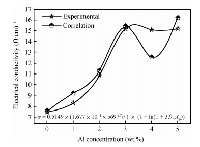
Fig. 1.
The experimental electrical conductivity and correlation of ZnO:Al thin films as a function of the Al concentration.
SEMICONDUCTOR MATERIALS
Said Benramache, Okba Belahssen and Hachemi Ben Temam
Corresponding author: Said Benramache, Email:benramache.said@gmail.com
Abstract: The transparent conductive pure and doped zinc oxide thin films with aluminum, cobalt and indium were deposited by ultrasonic spray technique on glass substrate at 350℃. This paper is to present a new approach to the description of correlation between electrical conductivity and optical gap energy with dopants' concentration of Al, Co and In. The correlation between the electrical and optical properties with doping level suggests that the electrical conductivity of the films is predominantly estimated by the band gap energy and the concentrations of Al, Co and In. The measurement in the electrical conductivity of doped films with correlation is equal to the experimental value, the error of this correlation is smaller than 13%. The minimum error value was estimated in the cobalt-doped ZnO thin films. This result indicates that such Co-doped ZnO thin films are chemically purer and have far fewer defects and less disorder owing to an almost complete chemical decomposition.
Keywords: ZnO, thin films, semiconductor doping, electrical conductivity, optical gap energy, correlation
| [1] |
Benramache S, Benhaoua B, Chabane F, et al. Influence of growth time on crystalline structure, conductivity and optical properties of ZnO thin films. Journal of Semiconductors, 2013, 34(2): 023001 doi: 10.1088/1674-4926/34/2/023001
|
| [2] |
Benramache S, Rahal A, Benhaoua B. The effects of solvent nature on spray-deposited ZnO thin film prepared from Zn(CH3COO)2·2H2O. Optik, 2013, 125(2): 663 http://www.sciencedirect.com/science/article/pii/S0030402613010681
|
| [3] |
Crossay A, Buecheler S, Kranz L, et al. Spray-deposited Al-doped ZnO transparent contacts for CdTe solar cells. Solar Energy Materials & Solar Cells, 2012, 101(4): 283 http://www.sciencedirect.com/science/article/pii/S0927024812000669
|
| [4] |
Zhang Yong'ai, Wu Chaoxing, Zheng Yong, et al. Synthesis and efficient field emission characteristics of patterned ZnO nanowires. Journal of Semiconductors, 2012, 33(2): 023001 doi: 10.1088/1674-4926/33/2/023001
|
| [5] |
Zhang Huafu, Liu Hanfa, Lei Chengxin, et al. Low-temperature deposition of transparent conducting Mn-W co-doped ZnO thin films. Journal of Semiconductors, 2010, 31(8): 083005 doi: 10.1088/1674-4926/31/8/083005
|
| [6] |
Benhaoua B, Rahal A, Benramache S. The structural, optical and electrical properties of nanocrystalline ZnO:Al thin films. Superlattices and Microstructures, 2014, 68: 38 doi: 10.1016/j.spmi.2014.01.005
|
| [7] |
Ma L, Ai X, Huang X, et al. Effects of the substrate and oxygen partial pressure on the microstructures and optical properties of Ti-doped ZnO thin films. Superlattices and Microstructures, 2011, 50(4): 703 http://www.sciencedirect.com/science/article/pii/S0749603611001844
|
| [8] |
Wang S K, Lin T C, Jian S R, et al. Effects of post-annealing on the structural and nanomechanical properties of Ga-doped ZnO thin films deposited on glass substrate by RF-magnetron sputtering. Appl Surf Sci, 2011, 258(4): 1261 http://www.sciencedirect.com/science/article/pii/S0169433211014905?_rdoc=44&_fmt=high&_origin=browse&_srch=hubEid(1-s2.0-S0169433211X0020X)&_docanchor=&_ct=47&_refLink=Y&_zone=rslt_list_item&md5=2d585874de4da99bc30563146e2d5bb4
|
| [9] |
Ilican S, Caglar Y, Caglar M, et al. Electrical conductivity, optical and structural properties of indium-doped ZnO nanofiber thin film deposited by spray pyrolysis method. Phys E, 2006, 35(1): 131 doi: 10.1016/j.physe.2006.07.009
|
| [10] |
Hafdallah A, Yanineb F, Aida M S, et al. In doped ZnO thin films. Journal of Alloys and Compounds, 2011, 509(18): 7267 http://www.sciencedirect.com/science/article/pii/S0925838811008954
|
| [11] |
Rahmane S, Djouadi M A, Aida M S, et al. Power and pressure effects upon magnetron sputtered aluminum doped ZnO films properties. Thin Solid Films, 2010, 519(1): 5 doi: 10.1016/j.tsf.2010.06.063
|
| [12] |
Van L H, Hong M H, Ding J. Structural and magnetic property of Co doped ZnO thin films prepared by pulsed laser deposition. Journal of Alloys and Compounds, 2008, 449(1): 207 http://www.sciencedirect.com/science/article/pii/S0925838806020834
|
| [13] |
Zhu Xiaming, Wu Huizhen, Wang Shuangjiang, et al. Optical and electrical properties of N-doped ZnO and fabrication of thin-film transistors. Journal of Semiconductors, 2009, 30(3): 033001 doi: 10.1088/1674-4926/30/3/033001
|
| [14] |
Rozati S M, Akesteh S. Characterization of ZnO:Al thin films obtained by spray pyrolysis technique. Materials Characterization, 2007, 58(3): 319 http://www.sciencedirect.com/science/article/pii/S104458030600180X
|
| [15] |
Ma Q B, Ye Z Z, He H P, et al. Preparation and characterization of transparent conductive ZnO:Ga films by DC reactive magnetron sputtering. Materials Characterization, 2008, 59(2): 124 doi: 10.1016/j.matchar.2006.11.020
|
| [16] |
Wojtczak L, Romanowski S, Stasiak W, et al. Correlation in calculations of density of states in thin films. Czech Journal Physics B, 1981, 31(12): 1024 doi: 10.1007/BF01598466
|
| [17] |
Tudose I V, Horvath P, Suchea M, et al. Correlation of ZnO thin film surface properties with conductivity. Appl Phys, 2007, 89(1): 57 doi: 10.1007/s00339-007-4036-3
|
| [18] |
Benramache S, Belahssen O, Arif A, et al. A correlation for crystallite size of undoped ZnO thin film with the band gap energy-precursor molarity-substrate temperature. Optik, 2014, 125(4): 1303 http://www.sciencedirect.com/science/article/pii/S0030402613011789
|
| [19] |
Benramache S, Belahssen O, Guettaf Arif A. Study on the correlation between crystallite size-optical gap energy and precursor molarities of ZnO thin films. Journal of Semiconductors, 2013, 35(4): 043001 http://www.jos.ac.cn/bdtxbcn/ch/reader/view_abstract.aspx?flag=1&file_no=13101401&journal_id=bdtxbcn
|
| [20] |
Joshi B, Ghosh S, Srivastava P, et al. Correlation between electrical transport, microstructure and room temperature ferromagnetism in 200 keV Ni2+ ion implanted zinc oxide (ZnO) thin films. Appl Phys, 2012, 107(2): 393 doi: 10.1007/s00339-012-6785-x
|
| [21] |
Wang SD, Miyadera T, Minari T, et al. Correlation between grain size and device parameters in pentacene thin film transistors. Appl Phys Lett, 2008, 93(4): 043311 doi: 10.1063/1.2967193
|
| [22] |
Minami T, Nanto H, Takata S. Correlation between film quality and photoluminescence in sputtered ZnO thin films. J Mater Sci, 1982, 17(5): 1364 doi: 10.1007/BF00752247
|
| [23] |
Zhu J J, Vines L, Aaltonen T, et al. Correlation between nitrogen and carbon in corporation into MOVPE ZnO at various oxidizing conditions. Microelectron J, 2009, 40(2): 232 doi: 10.1016/j.mejo.2008.07.042
|
| [24] |
Deng R, Zou Y, Tang H. Correlation between electrical, optical properties and Ag2+ centers of ZnO:Ag thin films. Physica B, 2008, 403(6): 2004 http://www.sciencedirect.com/science/article/pii/S0921452607012987
|
| [25] |
Ajimsha R S, Das A K, Singh B N, et al. Correlation between electrical and optical properties of Cr:ZnO thin films grown by pulsed laser deposition. Physica B, 2011, 406(12): 4578 http://www.sciencedirect.com/science/article/pii/S0921452611008969
|
| [26] |
Ton-That C, Foley M, Phillips M R, et al. Correlation between the structural and optical properties of Mn-doped ZnO nanoparticles. Journal of Alloys and Compounds, 2012, 522(1): 114 http://www.sciencedirect.com/science/article/pii/S0925838812001880
|
| [27] |
Ivill M, Pearton S J, Norton D P, et al. Magnetization dependence on electron density in epitaxial ZnO thin films codoped with Mn and Sn. J Appl Phys, 2005, 97(5): 53904 doi: 10.1063/1.1856225
|
| [28] |
Vollmann W, Berger W, Hamann C, et al. Relations between the morphology and conductivity of thin films of tetrathiofulvaliniumtetracyanoquinodimethane. Thin Solid Films, 1984, 111(1): 7 doi: 10.1016/0040-6090(84)90344-4
|
| [29] |
Asadov A, Gao W, Li Z, et al. Correlation between structural and electrical properties of ZnO thin films. Thin Solid Films, 2005, 476(1): 201 doi: 10.1016/j.tsf.2004.09.038
|
| [30] |
Gahtar A, Benramache S, Benhaoua B, et al. Preparation of transparent conducting ZnO:Al films on glass substrates by ultrasonic spray technique. Journal of Semiconductors, 2013, 34(7): 073001 doi: 10.1088/1674-4926/34/7/073001
|
| [31] |
Benramache S, Benhaoua B, Bentrah H. Preparation of transparent conducting of ZnO:Co and ZnO:In thin films by ultrasonic spray method. Journal of Nanostructure in Chemistry, 2013, 3(54): 1 http://kns.cnki.net/KCMS/detail/detail.aspx?filename=bdtx201307008&dbname=CJFD&dbcode=CJFQ
|
| [32] |
Benramache S, Benhaoua B, Chabane F. Effect of substrate temperature on the stability of transparent conducting cobalt doped ZnO thin films. Journal of Semiconductors, 2012, 33(9): 093001 doi: 10.1088/1674-4926/33/9/093001
|
| [33] |
Benramache S, Benhaoua B. Influence of substrate temperature and Cobalt concentration on structural and optical properties of ZnO thin films prepared by ultrasonic spray technique. Superlattices and Microstructures, 2012, 52(4): 807 doi: 10.1016/j.spmi.2012.06.005
|
| [34] |
Benramache S, Benhaoua B. Influence of annealing temperature on structural and optical properties of ZnO: In thin films prepared by ultrasonic spray technique. Superlattices and Microstructures. 2012, 52(6): 1062 doi: 10.1016/j.spmi.2012.08.006
|
| [35] |
Benramache S, Belahssen O, Guettaf A, et al. Correlation between electrical conductivity-optical band gap energy and precursor molarities ultrasonic spray deposition of ZnO thin films. Journal of Semiconductors, 2013, 34(11): 113001 doi: 10.1088/1674-4926/34/11/113001
|
Table 1.
The band gap energy

|
Table 2. The variation of empirical constants estimated by Eq. (3) of ZnO:Al, ZnO:Co and ZnO:In.

|
Table 3.
The experimental electrical conductivity

|
| [1] |
Benramache S, Benhaoua B, Chabane F, et al. Influence of growth time on crystalline structure, conductivity and optical properties of ZnO thin films. Journal of Semiconductors, 2013, 34(2): 023001 doi: 10.1088/1674-4926/34/2/023001
|
| [2] |
Benramache S, Rahal A, Benhaoua B. The effects of solvent nature on spray-deposited ZnO thin film prepared from Zn(CH3COO)2·2H2O. Optik, 2013, 125(2): 663 http://www.sciencedirect.com/science/article/pii/S0030402613010681
|
| [3] |
Crossay A, Buecheler S, Kranz L, et al. Spray-deposited Al-doped ZnO transparent contacts for CdTe solar cells. Solar Energy Materials & Solar Cells, 2012, 101(4): 283 http://www.sciencedirect.com/science/article/pii/S0927024812000669
|
| [4] |
Zhang Yong'ai, Wu Chaoxing, Zheng Yong, et al. Synthesis and efficient field emission characteristics of patterned ZnO nanowires. Journal of Semiconductors, 2012, 33(2): 023001 doi: 10.1088/1674-4926/33/2/023001
|
| [5] |
Zhang Huafu, Liu Hanfa, Lei Chengxin, et al. Low-temperature deposition of transparent conducting Mn-W co-doped ZnO thin films. Journal of Semiconductors, 2010, 31(8): 083005 doi: 10.1088/1674-4926/31/8/083005
|
| [6] |
Benhaoua B, Rahal A, Benramache S. The structural, optical and electrical properties of nanocrystalline ZnO:Al thin films. Superlattices and Microstructures, 2014, 68: 38 doi: 10.1016/j.spmi.2014.01.005
|
| [7] |
Ma L, Ai X, Huang X, et al. Effects of the substrate and oxygen partial pressure on the microstructures and optical properties of Ti-doped ZnO thin films. Superlattices and Microstructures, 2011, 50(4): 703 http://www.sciencedirect.com/science/article/pii/S0749603611001844
|
| [8] |
Wang S K, Lin T C, Jian S R, et al. Effects of post-annealing on the structural and nanomechanical properties of Ga-doped ZnO thin films deposited on glass substrate by RF-magnetron sputtering. Appl Surf Sci, 2011, 258(4): 1261 http://www.sciencedirect.com/science/article/pii/S0169433211014905?_rdoc=44&_fmt=high&_origin=browse&_srch=hubEid(1-s2.0-S0169433211X0020X)&_docanchor=&_ct=47&_refLink=Y&_zone=rslt_list_item&md5=2d585874de4da99bc30563146e2d5bb4
|
| [9] |
Ilican S, Caglar Y, Caglar M, et al. Electrical conductivity, optical and structural properties of indium-doped ZnO nanofiber thin film deposited by spray pyrolysis method. Phys E, 2006, 35(1): 131 doi: 10.1016/j.physe.2006.07.009
|
| [10] |
Hafdallah A, Yanineb F, Aida M S, et al. In doped ZnO thin films. Journal of Alloys and Compounds, 2011, 509(18): 7267 http://www.sciencedirect.com/science/article/pii/S0925838811008954
|
| [11] |
Rahmane S, Djouadi M A, Aida M S, et al. Power and pressure effects upon magnetron sputtered aluminum doped ZnO films properties. Thin Solid Films, 2010, 519(1): 5 doi: 10.1016/j.tsf.2010.06.063
|
| [12] |
Van L H, Hong M H, Ding J. Structural and magnetic property of Co doped ZnO thin films prepared by pulsed laser deposition. Journal of Alloys and Compounds, 2008, 449(1): 207 http://www.sciencedirect.com/science/article/pii/S0925838806020834
|
| [13] |
Zhu Xiaming, Wu Huizhen, Wang Shuangjiang, et al. Optical and electrical properties of N-doped ZnO and fabrication of thin-film transistors. Journal of Semiconductors, 2009, 30(3): 033001 doi: 10.1088/1674-4926/30/3/033001
|
| [14] |
Rozati S M, Akesteh S. Characterization of ZnO:Al thin films obtained by spray pyrolysis technique. Materials Characterization, 2007, 58(3): 319 http://www.sciencedirect.com/science/article/pii/S104458030600180X
|
| [15] |
Ma Q B, Ye Z Z, He H P, et al. Preparation and characterization of transparent conductive ZnO:Ga films by DC reactive magnetron sputtering. Materials Characterization, 2008, 59(2): 124 doi: 10.1016/j.matchar.2006.11.020
|
| [16] |
Wojtczak L, Romanowski S, Stasiak W, et al. Correlation in calculations of density of states in thin films. Czech Journal Physics B, 1981, 31(12): 1024 doi: 10.1007/BF01598466
|
| [17] |
Tudose I V, Horvath P, Suchea M, et al. Correlation of ZnO thin film surface properties with conductivity. Appl Phys, 2007, 89(1): 57 doi: 10.1007/s00339-007-4036-3
|
| [18] |
Benramache S, Belahssen O, Arif A, et al. A correlation for crystallite size of undoped ZnO thin film with the band gap energy-precursor molarity-substrate temperature. Optik, 2014, 125(4): 1303 http://www.sciencedirect.com/science/article/pii/S0030402613011789
|
| [19] |
Benramache S, Belahssen O, Guettaf Arif A. Study on the correlation between crystallite size-optical gap energy and precursor molarities of ZnO thin films. Journal of Semiconductors, 2013, 35(4): 043001 http://www.jos.ac.cn/bdtxbcn/ch/reader/view_abstract.aspx?flag=1&file_no=13101401&journal_id=bdtxbcn
|
| [20] |
Joshi B, Ghosh S, Srivastava P, et al. Correlation between electrical transport, microstructure and room temperature ferromagnetism in 200 keV Ni2+ ion implanted zinc oxide (ZnO) thin films. Appl Phys, 2012, 107(2): 393 doi: 10.1007/s00339-012-6785-x
|
| [21] |
Wang SD, Miyadera T, Minari T, et al. Correlation between grain size and device parameters in pentacene thin film transistors. Appl Phys Lett, 2008, 93(4): 043311 doi: 10.1063/1.2967193
|
| [22] |
Minami T, Nanto H, Takata S. Correlation between film quality and photoluminescence in sputtered ZnO thin films. J Mater Sci, 1982, 17(5): 1364 doi: 10.1007/BF00752247
|
| [23] |
Zhu J J, Vines L, Aaltonen T, et al. Correlation between nitrogen and carbon in corporation into MOVPE ZnO at various oxidizing conditions. Microelectron J, 2009, 40(2): 232 doi: 10.1016/j.mejo.2008.07.042
|
| [24] |
Deng R, Zou Y, Tang H. Correlation between electrical, optical properties and Ag2+ centers of ZnO:Ag thin films. Physica B, 2008, 403(6): 2004 http://www.sciencedirect.com/science/article/pii/S0921452607012987
|
| [25] |
Ajimsha R S, Das A K, Singh B N, et al. Correlation between electrical and optical properties of Cr:ZnO thin films grown by pulsed laser deposition. Physica B, 2011, 406(12): 4578 http://www.sciencedirect.com/science/article/pii/S0921452611008969
|
| [26] |
Ton-That C, Foley M, Phillips M R, et al. Correlation between the structural and optical properties of Mn-doped ZnO nanoparticles. Journal of Alloys and Compounds, 2012, 522(1): 114 http://www.sciencedirect.com/science/article/pii/S0925838812001880
|
| [27] |
Ivill M, Pearton S J, Norton D P, et al. Magnetization dependence on electron density in epitaxial ZnO thin films codoped with Mn and Sn. J Appl Phys, 2005, 97(5): 53904 doi: 10.1063/1.1856225
|
| [28] |
Vollmann W, Berger W, Hamann C, et al. Relations between the morphology and conductivity of thin films of tetrathiofulvaliniumtetracyanoquinodimethane. Thin Solid Films, 1984, 111(1): 7 doi: 10.1016/0040-6090(84)90344-4
|
| [29] |
Asadov A, Gao W, Li Z, et al. Correlation between structural and electrical properties of ZnO thin films. Thin Solid Films, 2005, 476(1): 201 doi: 10.1016/j.tsf.2004.09.038
|
| [30] |
Gahtar A, Benramache S, Benhaoua B, et al. Preparation of transparent conducting ZnO:Al films on glass substrates by ultrasonic spray technique. Journal of Semiconductors, 2013, 34(7): 073001 doi: 10.1088/1674-4926/34/7/073001
|
| [31] |
Benramache S, Benhaoua B, Bentrah H. Preparation of transparent conducting of ZnO:Co and ZnO:In thin films by ultrasonic spray method. Journal of Nanostructure in Chemistry, 2013, 3(54): 1 http://kns.cnki.net/KCMS/detail/detail.aspx?filename=bdtx201307008&dbname=CJFD&dbcode=CJFQ
|
| [32] |
Benramache S, Benhaoua B, Chabane F. Effect of substrate temperature on the stability of transparent conducting cobalt doped ZnO thin films. Journal of Semiconductors, 2012, 33(9): 093001 doi: 10.1088/1674-4926/33/9/093001
|
| [33] |
Benramache S, Benhaoua B. Influence of substrate temperature and Cobalt concentration on structural and optical properties of ZnO thin films prepared by ultrasonic spray technique. Superlattices and Microstructures, 2012, 52(4): 807 doi: 10.1016/j.spmi.2012.06.005
|
| [34] |
Benramache S, Benhaoua B. Influence of annealing temperature on structural and optical properties of ZnO: In thin films prepared by ultrasonic spray technique. Superlattices and Microstructures. 2012, 52(6): 1062 doi: 10.1016/j.spmi.2012.08.006
|
| [35] |
Benramache S, Belahssen O, Guettaf A, et al. Correlation between electrical conductivity-optical band gap energy and precursor molarities ultrasonic spray deposition of ZnO thin films. Journal of Semiconductors, 2013, 34(11): 113001 doi: 10.1088/1674-4926/34/11/113001
|


Article views: 3871 Times PDF downloads: 51 Times Cited by: 0 Times
Received: 09 July 2013 Revised: 19 January 2014 Online: Published: 01 July 2014
| Citation: |
Said Benramache, Okba Belahssen, Hachemi Ben Temam. Effect of band gap energy on the electrical conductivity in doped ZnO thin film[J]. Journal of Semiconductors, 2014, 35(7): 073001. doi: 10.1088/1674-4926/35/7/073001
****
S Benramache, O Belahssen, H B Temam. Effect of band gap energy on the electrical conductivity in doped ZnO thin film[J]. J. Semicond., 2014, 35(7): 073001. doi: 10.1088/1674-4926/35/7/073001.

|
| [1] |
Benramache S, Benhaoua B, Chabane F, et al. Influence of growth time on crystalline structure, conductivity and optical properties of ZnO thin films. Journal of Semiconductors, 2013, 34(2): 023001 doi: 10.1088/1674-4926/34/2/023001
|
| [2] |
Benramache S, Rahal A, Benhaoua B. The effects of solvent nature on spray-deposited ZnO thin film prepared from Zn(CH3COO)2·2H2O. Optik, 2013, 125(2): 663 http://www.sciencedirect.com/science/article/pii/S0030402613010681
|
| [3] |
Crossay A, Buecheler S, Kranz L, et al. Spray-deposited Al-doped ZnO transparent contacts for CdTe solar cells. Solar Energy Materials & Solar Cells, 2012, 101(4): 283 http://www.sciencedirect.com/science/article/pii/S0927024812000669
|
| [4] |
Zhang Yong'ai, Wu Chaoxing, Zheng Yong, et al. Synthesis and efficient field emission characteristics of patterned ZnO nanowires. Journal of Semiconductors, 2012, 33(2): 023001 doi: 10.1088/1674-4926/33/2/023001
|
| [5] |
Zhang Huafu, Liu Hanfa, Lei Chengxin, et al. Low-temperature deposition of transparent conducting Mn-W co-doped ZnO thin films. Journal of Semiconductors, 2010, 31(8): 083005 doi: 10.1088/1674-4926/31/8/083005
|
| [6] |
Benhaoua B, Rahal A, Benramache S. The structural, optical and electrical properties of nanocrystalline ZnO:Al thin films. Superlattices and Microstructures, 2014, 68: 38 doi: 10.1016/j.spmi.2014.01.005
|
| [7] |
Ma L, Ai X, Huang X, et al. Effects of the substrate and oxygen partial pressure on the microstructures and optical properties of Ti-doped ZnO thin films. Superlattices and Microstructures, 2011, 50(4): 703 http://www.sciencedirect.com/science/article/pii/S0749603611001844
|
| [8] |
Wang S K, Lin T C, Jian S R, et al. Effects of post-annealing on the structural and nanomechanical properties of Ga-doped ZnO thin films deposited on glass substrate by RF-magnetron sputtering. Appl Surf Sci, 2011, 258(4): 1261 http://www.sciencedirect.com/science/article/pii/S0169433211014905?_rdoc=44&_fmt=high&_origin=browse&_srch=hubEid(1-s2.0-S0169433211X0020X)&_docanchor=&_ct=47&_refLink=Y&_zone=rslt_list_item&md5=2d585874de4da99bc30563146e2d5bb4
|
| [9] |
Ilican S, Caglar Y, Caglar M, et al. Electrical conductivity, optical and structural properties of indium-doped ZnO nanofiber thin film deposited by spray pyrolysis method. Phys E, 2006, 35(1): 131 doi: 10.1016/j.physe.2006.07.009
|
| [10] |
Hafdallah A, Yanineb F, Aida M S, et al. In doped ZnO thin films. Journal of Alloys and Compounds, 2011, 509(18): 7267 http://www.sciencedirect.com/science/article/pii/S0925838811008954
|
| [11] |
Rahmane S, Djouadi M A, Aida M S, et al. Power and pressure effects upon magnetron sputtered aluminum doped ZnO films properties. Thin Solid Films, 2010, 519(1): 5 doi: 10.1016/j.tsf.2010.06.063
|
| [12] |
Van L H, Hong M H, Ding J. Structural and magnetic property of Co doped ZnO thin films prepared by pulsed laser deposition. Journal of Alloys and Compounds, 2008, 449(1): 207 http://www.sciencedirect.com/science/article/pii/S0925838806020834
|
| [13] |
Zhu Xiaming, Wu Huizhen, Wang Shuangjiang, et al. Optical and electrical properties of N-doped ZnO and fabrication of thin-film transistors. Journal of Semiconductors, 2009, 30(3): 033001 doi: 10.1088/1674-4926/30/3/033001
|
| [14] |
Rozati S M, Akesteh S. Characterization of ZnO:Al thin films obtained by spray pyrolysis technique. Materials Characterization, 2007, 58(3): 319 http://www.sciencedirect.com/science/article/pii/S104458030600180X
|
| [15] |
Ma Q B, Ye Z Z, He H P, et al. Preparation and characterization of transparent conductive ZnO:Ga films by DC reactive magnetron sputtering. Materials Characterization, 2008, 59(2): 124 doi: 10.1016/j.matchar.2006.11.020
|
| [16] |
Wojtczak L, Romanowski S, Stasiak W, et al. Correlation in calculations of density of states in thin films. Czech Journal Physics B, 1981, 31(12): 1024 doi: 10.1007/BF01598466
|
| [17] |
Tudose I V, Horvath P, Suchea M, et al. Correlation of ZnO thin film surface properties with conductivity. Appl Phys, 2007, 89(1): 57 doi: 10.1007/s00339-007-4036-3
|
| [18] |
Benramache S, Belahssen O, Arif A, et al. A correlation for crystallite size of undoped ZnO thin film with the band gap energy-precursor molarity-substrate temperature. Optik, 2014, 125(4): 1303 http://www.sciencedirect.com/science/article/pii/S0030402613011789
|
| [19] |
Benramache S, Belahssen O, Guettaf Arif A. Study on the correlation between crystallite size-optical gap energy and precursor molarities of ZnO thin films. Journal of Semiconductors, 2013, 35(4): 043001 http://www.jos.ac.cn/bdtxbcn/ch/reader/view_abstract.aspx?flag=1&file_no=13101401&journal_id=bdtxbcn
|
| [20] |
Joshi B, Ghosh S, Srivastava P, et al. Correlation between electrical transport, microstructure and room temperature ferromagnetism in 200 keV Ni2+ ion implanted zinc oxide (ZnO) thin films. Appl Phys, 2012, 107(2): 393 doi: 10.1007/s00339-012-6785-x
|
| [21] |
Wang SD, Miyadera T, Minari T, et al. Correlation between grain size and device parameters in pentacene thin film transistors. Appl Phys Lett, 2008, 93(4): 043311 doi: 10.1063/1.2967193
|
| [22] |
Minami T, Nanto H, Takata S. Correlation between film quality and photoluminescence in sputtered ZnO thin films. J Mater Sci, 1982, 17(5): 1364 doi: 10.1007/BF00752247
|
| [23] |
Zhu J J, Vines L, Aaltonen T, et al. Correlation between nitrogen and carbon in corporation into MOVPE ZnO at various oxidizing conditions. Microelectron J, 2009, 40(2): 232 doi: 10.1016/j.mejo.2008.07.042
|
| [24] |
Deng R, Zou Y, Tang H. Correlation between electrical, optical properties and Ag2+ centers of ZnO:Ag thin films. Physica B, 2008, 403(6): 2004 http://www.sciencedirect.com/science/article/pii/S0921452607012987
|
| [25] |
Ajimsha R S, Das A K, Singh B N, et al. Correlation between electrical and optical properties of Cr:ZnO thin films grown by pulsed laser deposition. Physica B, 2011, 406(12): 4578 http://www.sciencedirect.com/science/article/pii/S0921452611008969
|
| [26] |
Ton-That C, Foley M, Phillips M R, et al. Correlation between the structural and optical properties of Mn-doped ZnO nanoparticles. Journal of Alloys and Compounds, 2012, 522(1): 114 http://www.sciencedirect.com/science/article/pii/S0925838812001880
|
| [27] |
Ivill M, Pearton S J, Norton D P, et al. Magnetization dependence on electron density in epitaxial ZnO thin films codoped with Mn and Sn. J Appl Phys, 2005, 97(5): 53904 doi: 10.1063/1.1856225
|
| [28] |
Vollmann W, Berger W, Hamann C, et al. Relations between the morphology and conductivity of thin films of tetrathiofulvaliniumtetracyanoquinodimethane. Thin Solid Films, 1984, 111(1): 7 doi: 10.1016/0040-6090(84)90344-4
|
| [29] |
Asadov A, Gao W, Li Z, et al. Correlation between structural and electrical properties of ZnO thin films. Thin Solid Films, 2005, 476(1): 201 doi: 10.1016/j.tsf.2004.09.038
|
| [30] |
Gahtar A, Benramache S, Benhaoua B, et al. Preparation of transparent conducting ZnO:Al films on glass substrates by ultrasonic spray technique. Journal of Semiconductors, 2013, 34(7): 073001 doi: 10.1088/1674-4926/34/7/073001
|
| [31] |
Benramache S, Benhaoua B, Bentrah H. Preparation of transparent conducting of ZnO:Co and ZnO:In thin films by ultrasonic spray method. Journal of Nanostructure in Chemistry, 2013, 3(54): 1 http://kns.cnki.net/KCMS/detail/detail.aspx?filename=bdtx201307008&dbname=CJFD&dbcode=CJFQ
|
| [32] |
Benramache S, Benhaoua B, Chabane F. Effect of substrate temperature on the stability of transparent conducting cobalt doped ZnO thin films. Journal of Semiconductors, 2012, 33(9): 093001 doi: 10.1088/1674-4926/33/9/093001
|
| [33] |
Benramache S, Benhaoua B. Influence of substrate temperature and Cobalt concentration on structural and optical properties of ZnO thin films prepared by ultrasonic spray technique. Superlattices and Microstructures, 2012, 52(4): 807 doi: 10.1016/j.spmi.2012.06.005
|
| [34] |
Benramache S, Benhaoua B. Influence of annealing temperature on structural and optical properties of ZnO: In thin films prepared by ultrasonic spray technique. Superlattices and Microstructures. 2012, 52(6): 1062 doi: 10.1016/j.spmi.2012.08.006
|
| [35] |
Benramache S, Belahssen O, Guettaf A, et al. Correlation between electrical conductivity-optical band gap energy and precursor molarities ultrasonic spray deposition of ZnO thin films. Journal of Semiconductors, 2013, 34(11): 113001 doi: 10.1088/1674-4926/34/11/113001
|

 WeChat ID
Journal of Semiconductors © 2017 All Rights Reserved 京ICP备05085259号-2

 DownLoad:

