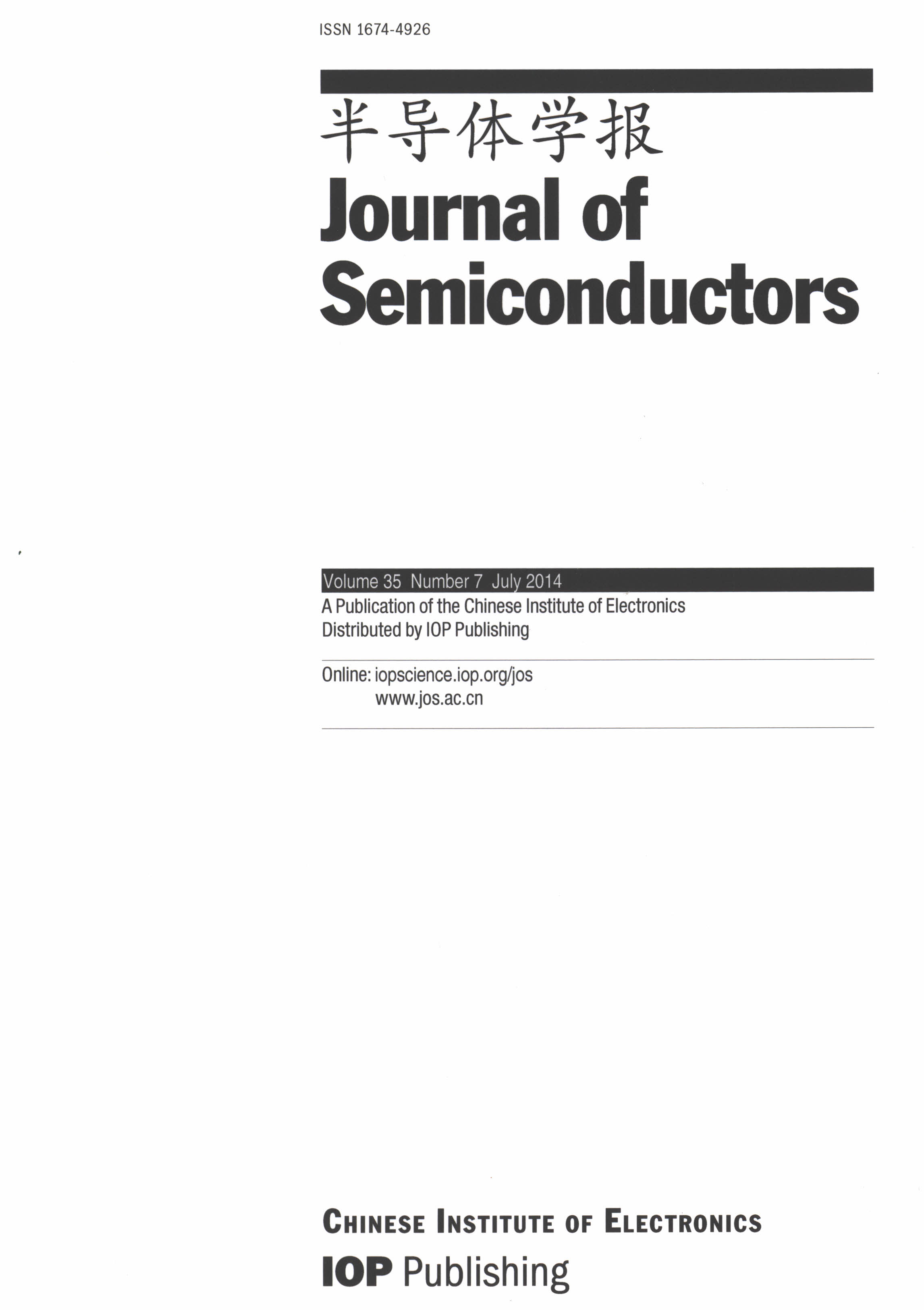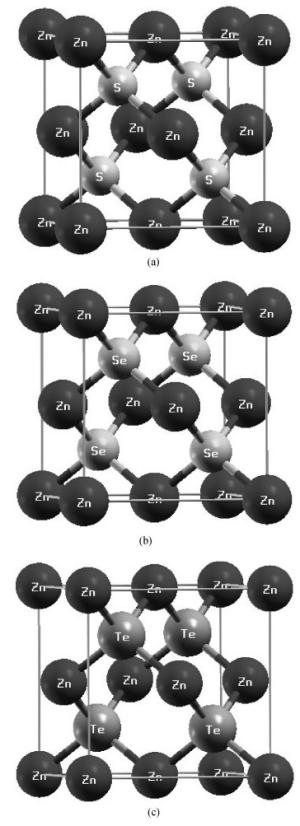
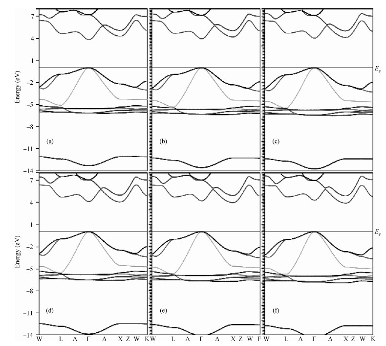
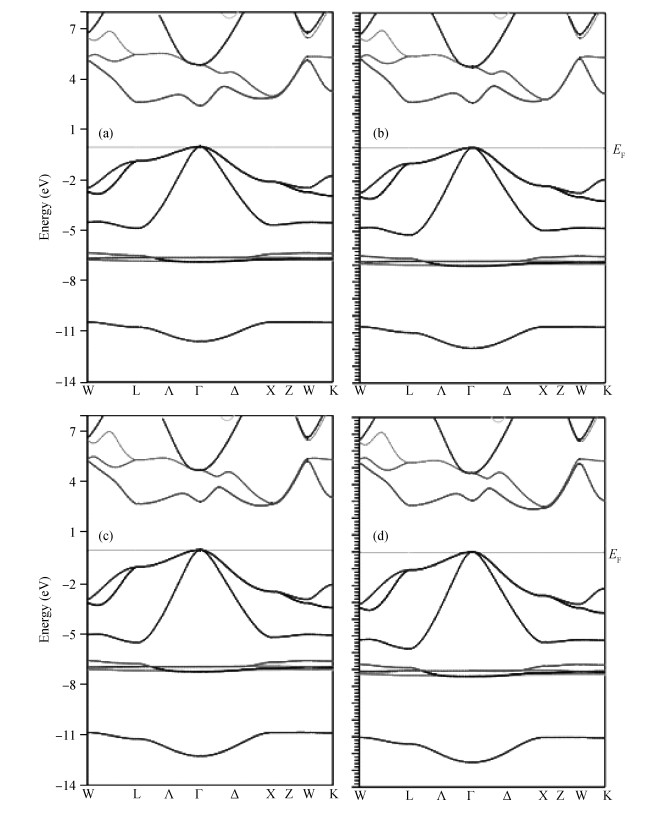
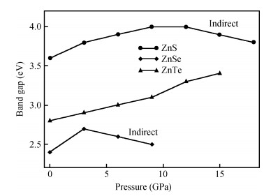
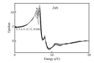
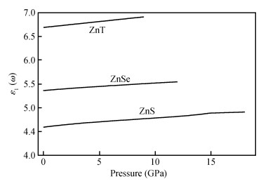
Structural, elastic, electronic and optical properties of zinc-chalcogenides (viz. ZnX, X=S, Se and Te) are studied in zinc-blende structure under hydrostatic pressure using the full-potential linearized augmented plane wave method. Generalized gradient approximation is used for exchange correlation potentials. Pressure-dependent lattice constants and bulk moduli are obtained using the optimization method. Young's modulus, Poisson's ratio, internal strain parameter and anisotropy are also calculated. The higher values of Young's modulus in comparison to the bulk modulus show that these materials are hard to break. Poisson's ratio is computed for the first time for these materials to the best of our knowledge and its values show higher ionic contribution in these materials. Modified Becke and Johnson (mBJ) method is used to study band gaps, density of states, dielectric function and refractive index. Electronic study shows direct band gaps convert to indirect band gaps with increasing pressure in the case of ZnS and ZnTe. We compared our results with other theoretical and experimental results. Our results are far better than other theoretical results because mBJ is the best technique to treat Ⅱ-Ⅵ semiconductors.


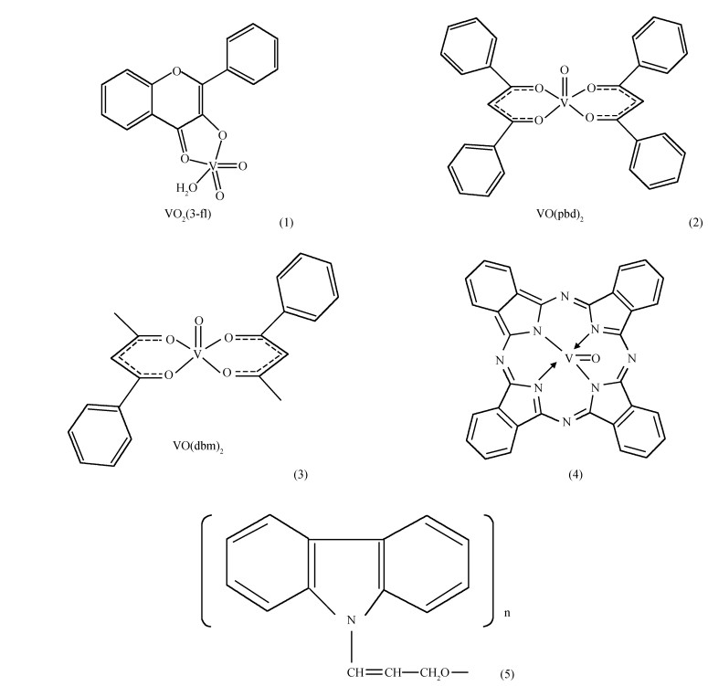
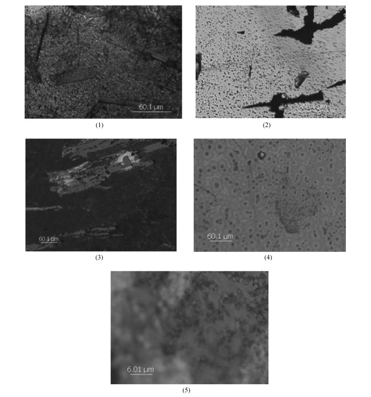
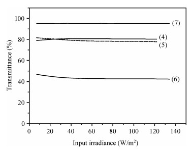
Thin films of five vanadium compounds/composite:(1) VO2(3-fl) (3-fl=3-Hydroxyflavone), (2) VO(pbd)2 (pbd=1-Phenyl-1, 3-butadione), (3) VO(dbm)2 (dbm=Dibenzoylmethane), (4) VPc (Vanadyl Phthalocyanine) and (5) V2O5-PEPC (V2O5-poly-N-epoxypropylcarbazole composite), were deposited by the drop-casting method from the solution in benzene. The transmittance-irradiance relationships were investigated and the transmission in the visible spectrum and optical images were obtained as well. It was found that the transmittance of the VO2(3-fl), VO(pbd)2, VO(dbm)2 and VPc, was practically independent of the irradiance; whereas the transmittance of V2O5-PEPC decreased by 4% for thin and 9% for thick film with an increase of the irradiance.

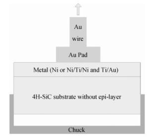
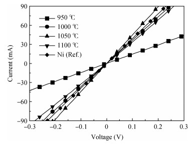
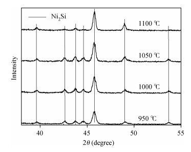
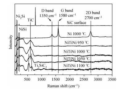
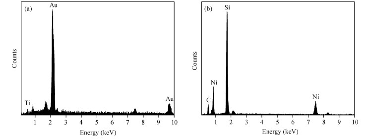
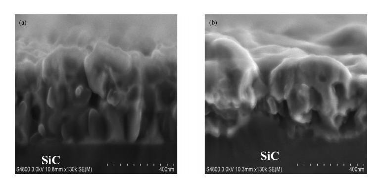
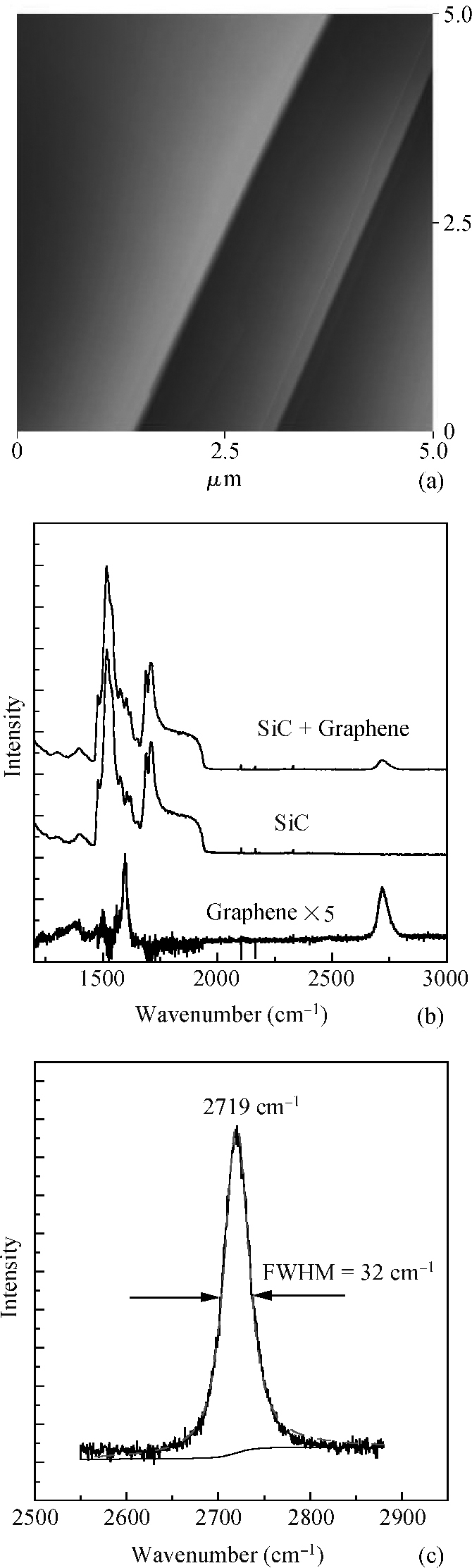
The Ni/Ti/Ni multilayer ohmic contact properties on a 4H-SiC substrate and improved adhesion with the Ti/Au overlayer have been investigated. The best specific contact resistivity of 3.16×10⁻⁵ Ω·cm2 was obtained at 1050℃. Compared with Ni/SiC ohmic contact, the adhesion between Ni/Ti/Ni/SiC and the Ti/Au overlayer was greatly improved and the physical mechanism under this behavior was analyzed by using Raman spectroscopy and X-ray energy dispersive spectroscopy (EDS) measurement. It is shown that a Ti-carbide and Ni-silicide compound exist at the surface and there is no graphitic carbon at the surface of the Ni/Ti/Ni structure by Raman spectroscopy, while a large amount of graphitic carbon appears at the surface of the Ni/SiC structure, which results in its bad adhesion. Moreover, the interface of the Ni/Ti/Ni/SiC is improved compared to the interface of Ni/SiC.

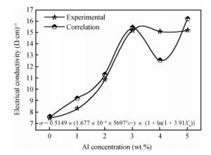
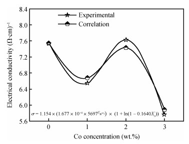
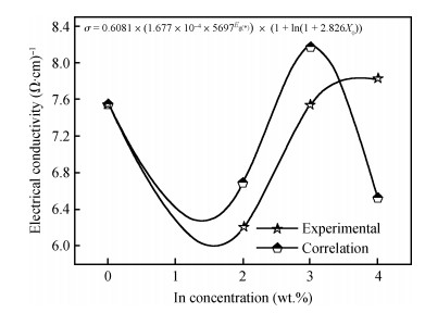
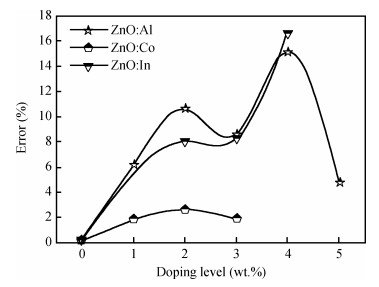
The transparent conductive pure and doped zinc oxide thin films with aluminum, cobalt and indium were deposited by ultrasonic spray technique on glass substrate at 350℃. This paper is to present a new approach to the description of correlation between electrical conductivity and optical gap energy with dopants' concentration of Al, Co and In. The correlation between the electrical and optical properties with doping level suggests that the electrical conductivity of the films is predominantly estimated by the band gap energy and the concentrations of Al, Co and In. The measurement in the electrical conductivity of doped films with correlation is equal to the experimental value, the error of this correlation is smaller than 13%. The minimum error value was estimated in the cobalt-doped ZnO thin films. This result indicates that such Co-doped ZnO thin films are chemically purer and have far fewer defects and less disorder owing to an almost complete chemical decomposition.

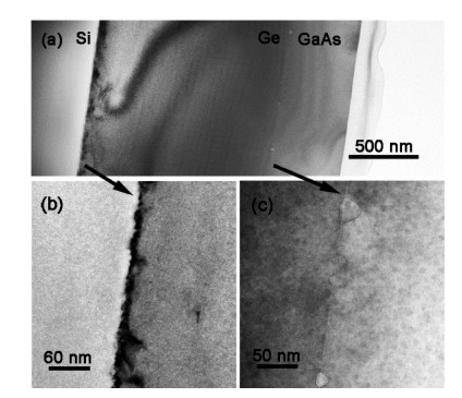
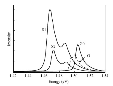
Device-quality GaAs thin films have been grown on miscut Ge-on-Si substrates by metal-organic chemical vapor deposition. A method of two-step epitaxy of GaAs is performed to achieve a high-quality top-layer. The initial thin buffer layer at 360℃ is critical for the suppression of anti-phase boundaries and threading dislocations. The etch pit density of GaAs epilayers by KOH etching could reach 2.25×105 cm-2 and high-quality GaAs top epilayers are observed by transmission electron microscopy. The band-to-band photoluminescence property of GaAs epilayers on different substrates is also investigated and negative band shifts of several to tens of meVs are found because of tensile strains in the GaAs epilayers. To achieve a smooth surface, a polishing process is performed, followed by a second epitaxy of GaAs. The root-mean-square roughness of the GaAs surface could be less than 1 nm, which is comparable with that of homo-epitaxial GaAs. These low-defect and smooth GaAs epilayers on Si are desirable for GaAs-based devices on silicon substrates.


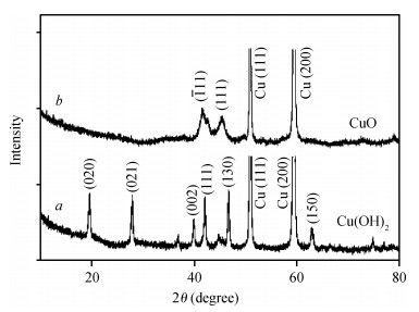
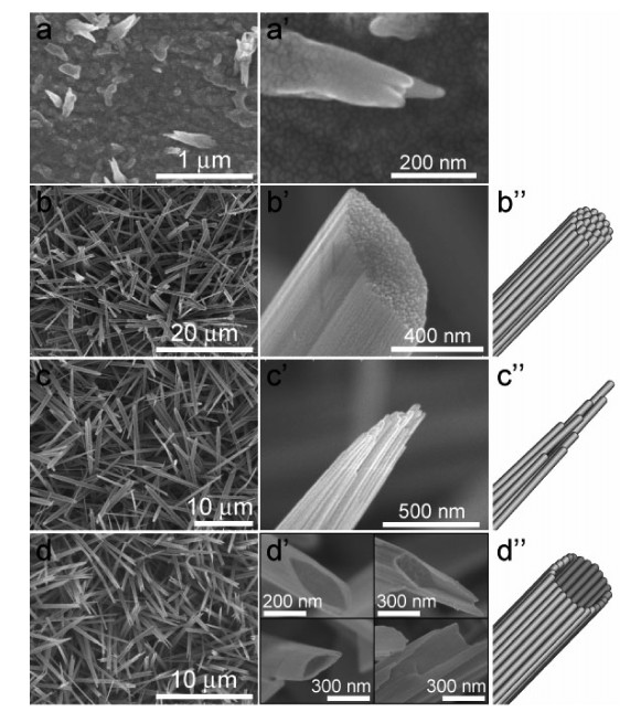
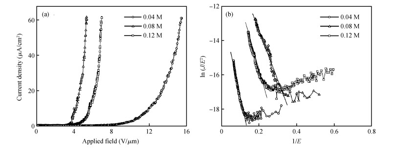
One-dimensional CuO nanostructure arrays have been synthesized on Cu foil by a low-temperature wet chemical process. Different CuO nanostructures including nanorods with facet heads, nanorods with needle-like tips and nanotubes are shaped simply by varying the concentration of oxidant. Field emission measurements show that CuO nanorods with needle-like tips are of superior performance than other shapes, having a turn-on field of 3.5 V/μm and a field enhancement factor of 2107. The good field emission performance is assigned to the sharp tips contributing to the high field enhancement effect and to the moderate density reducing the field screening effect.

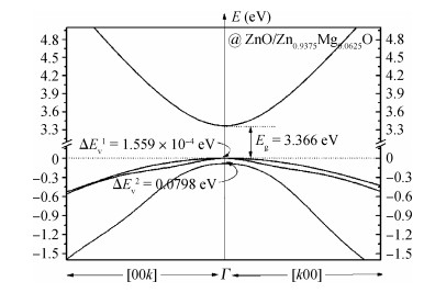
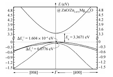
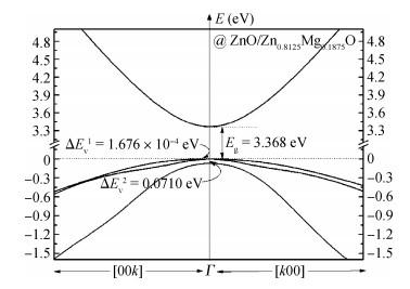
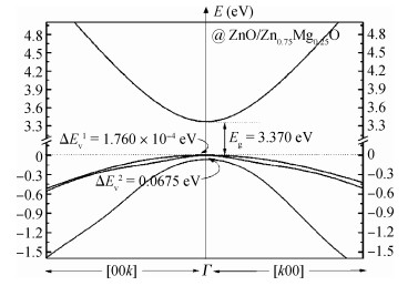
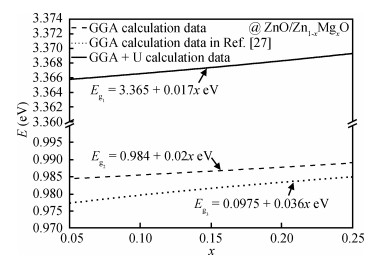
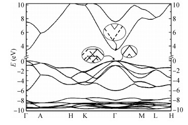
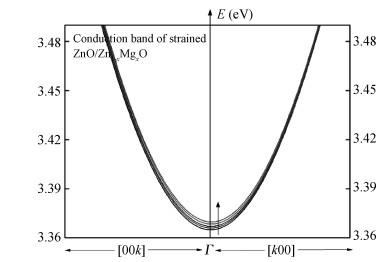
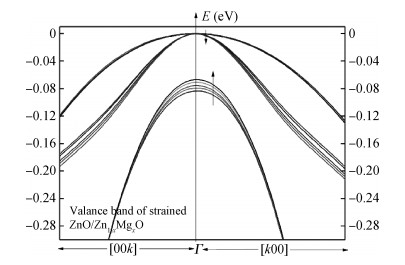
Band structures in wurtzite bulk ZnO/Zn1-xMgxO are calculated using first-principles based on the framework of generalized gradient approximation to density functional theory with the introduction of the on-site Coulomb interaction. Strain effects on band gap, splitting energies of valence bands, electron and hole effective masses in strained bulk ZnO are discussed. According to the results, the band gap increases gradually with increasing stress in strained ZnO as an Mg content of Zn1-xMgxO substrate less than 0.3, which is consistent with the experimental results. It is further demonstrated that electron mass of conduction band (CB) under stress increases slightly. There are almost no changes in effective masses of light hole band (LHB) and heavy hole band (HHB) along[00k] and[k00] directions under stress, and stress leads to an obvious decrease in effective masses of crystal splitting band (CSB) along the same directions.


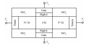
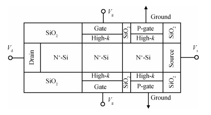
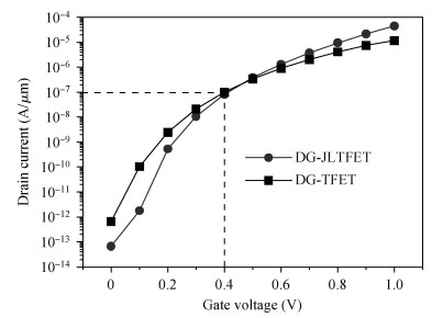
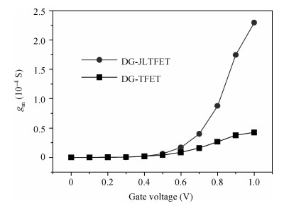
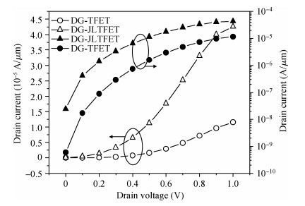
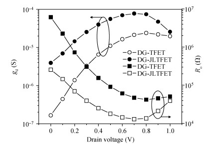
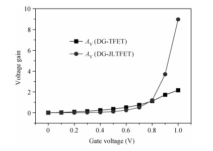
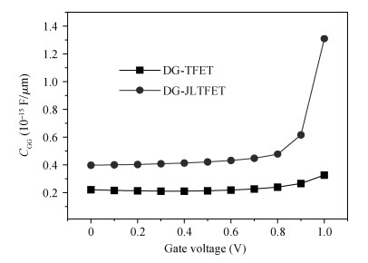
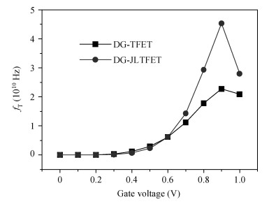
For the first time, we investigate the analog performance of n-type double gate junctionless tunnel field effect transistor (DG-JLTFET) and the results are compared with the conventional n-type double gate tunnel field effect transistor (DG-TFET) counterpart. Using extensive device simulations, the two devices are compared with the following analog performance parameters, namely transconductance, output conductance, output resistance, intrinsic gain, total gate capacitance and unity gain frequency. From the device simulation results, DG-JLTFET is found to have significantly better analog performance as compared to DG-TFET.

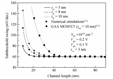
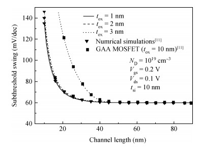
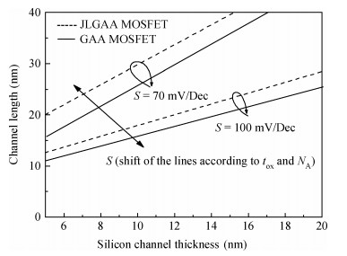
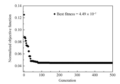
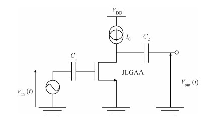
An analytical investigation has been proposed to study the subthreshold behavior of junctionless gates all around (JLGAA) MOSFET for nanoscale CMOS analog applications. Based on 2-D analytical analysis, a new subthreshold swing model for short-channel JLGAA MOSFETs is developed. The analysis has been used to calculate the subthreshold swing and to compare the performance of the investigated design and conventional GAA MOSFET, where the comparison of device architectures shows that the JLGAA MOSFET exhibits a superior performance with respect to the conventional inversion-mode GAA MOSFET in terms of the fabrication process and electrical behavior in the subthreshold domain. The analytical models have been validated by 2-D numerical simulations. The proposed analytical models are used to formulate the objectives functions. The overall objective function is formulated by means of a weighted sum approach to search the optimal electrical and dimensional device parameters in order to obtain the better scaling capability and the electrical performance of the device for ultra-low power applications.

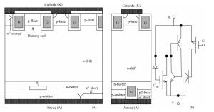
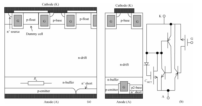
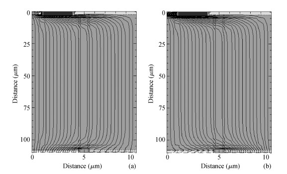
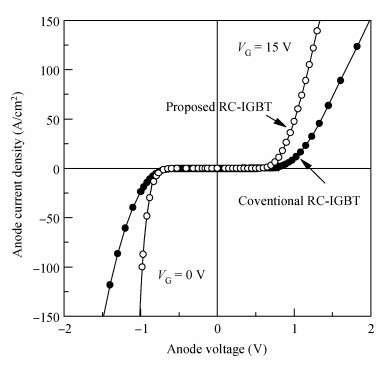
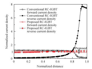
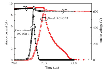
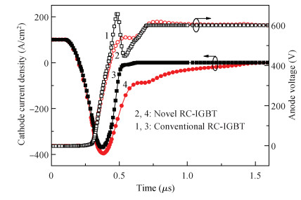
Novel reverse-conducting IGBT (RC-IGBT) with anti-parallel MOS controlled thyristor (MCT) is proposed. Its major feature is the introduction of an automatically controlled MCT at the anode, by which the anode-short effect is eliminated and the voltage snapback problem is solved. Furthermore, the snapback-free characteristics can be realized in novel RC-IGBT by a single cell with a width of 10 μm with more uniform current distribution. As numerical simulations show, compared with the conventional RC-IGBT, the forward conduction voltage is reduced by 35% while the reverse conduction voltage is reduced by 50% at J=150 A/cm2.

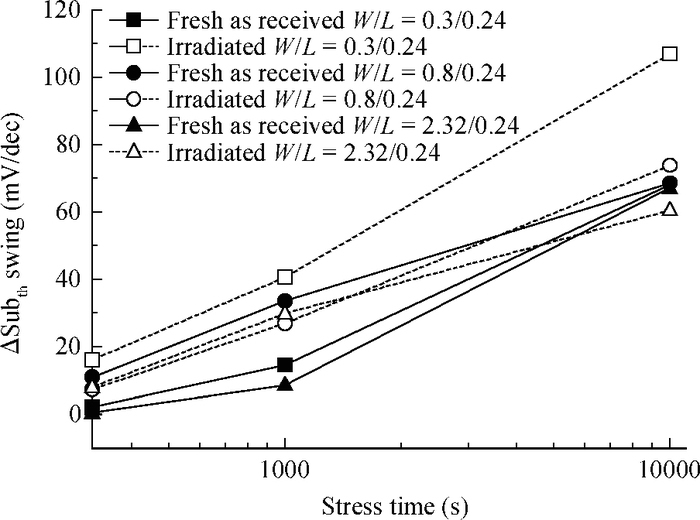
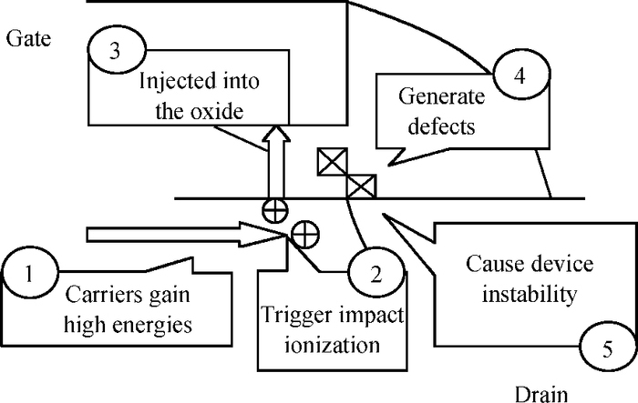
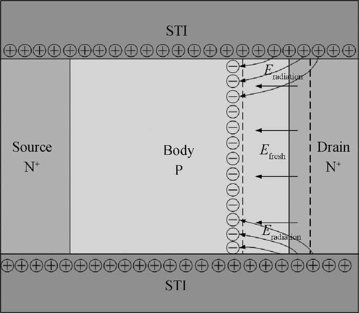
We investigate how γ exposure impacts the hot-carrier degradation in deep submicron NMOSFET with different technologies and device geometries for the first time. The results show that hot-carrier degradations on irradiated devices are greater than those without irradiation, especially for narrow channel device. The reason is attributed to charge traps in STI, which then induce different electric field and impact ionization rates during hot-carrier stress.


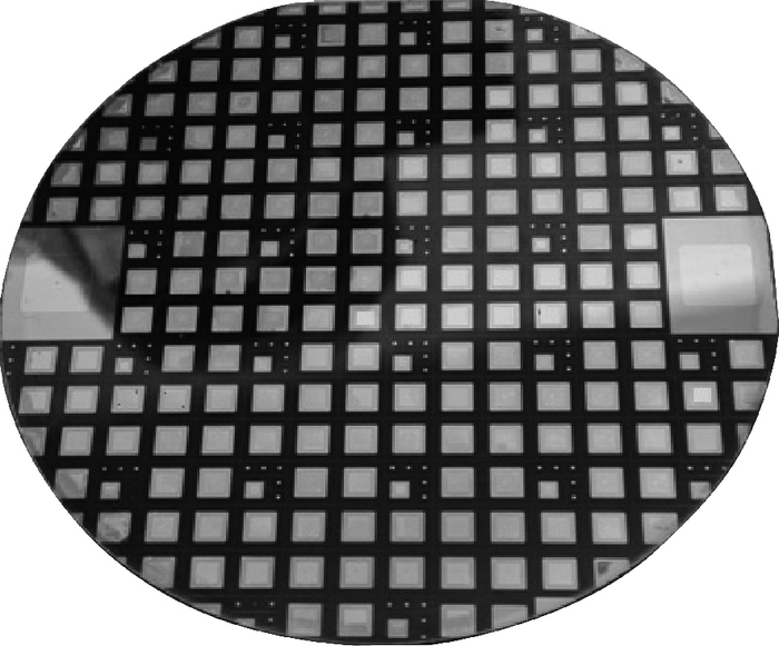
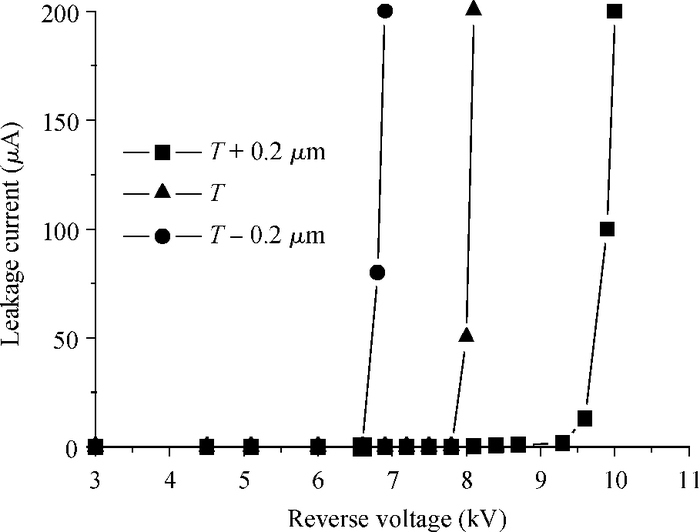
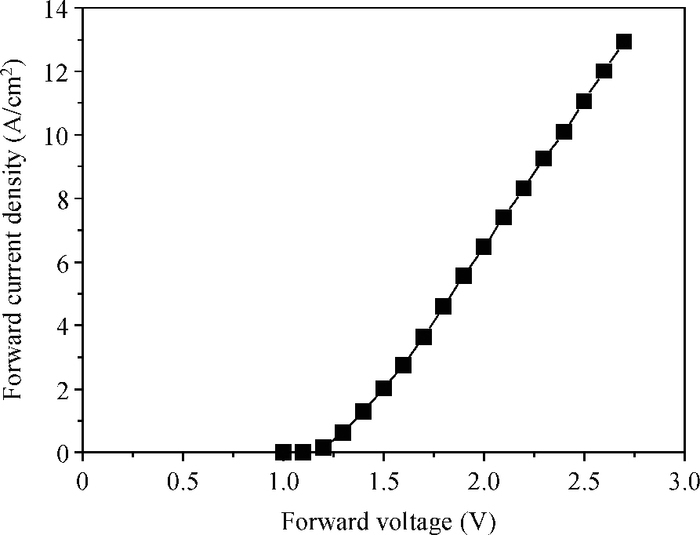
The design, fabrication, and electrical characteristics of the 4H-SiC JBS diode with a breakdown voltage higher than 10 kV are presented. 60 floating guard rings have been used in the fabrication. Numerical simulations have been performed to select the doping level and thickness of the drift layer and the effectiveness of the edge termination technique. The n-type epilayer is 100 μm in thickness with a doping of 6×1014 cm-3. The on-state voltage was 2.7 V at JF=13 A/cm2.


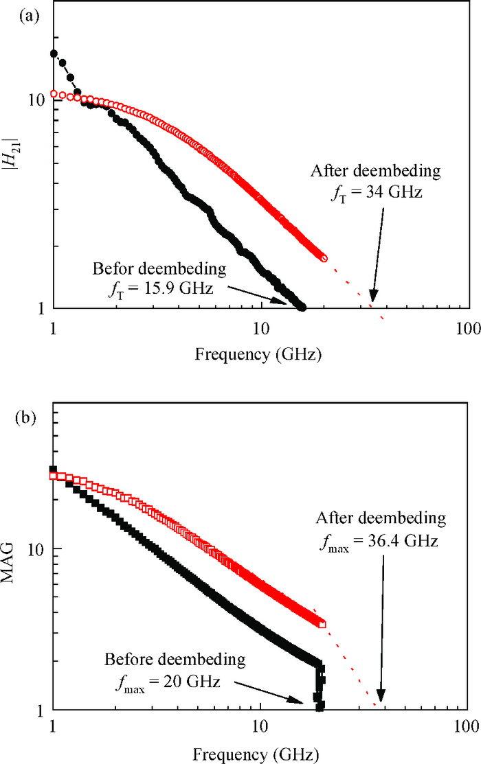
A scalable self-aligned approach is employed to fabricate monolayer graphene field-effect transistors on semi-insulated 4H-SiC (0001) substrates. The self-aligned process minimized access resistance and parasitic capacitance. Self-oxidized Al2O3, formed by deposition of 2 nm Al followed by exposure in air to be oxidized, is used as gate dielectric and shows excellent insulation. An intrinsic cutoff frequency of 34 GHz and maximum oscillation frequency of 36.4 GHz are realized for the monolayer graphene field-effect transistor with a gate length of 0.2 μm. These studies show a pathway to fabricate graphene transistors for future applications in ultra-high frequency circuits.


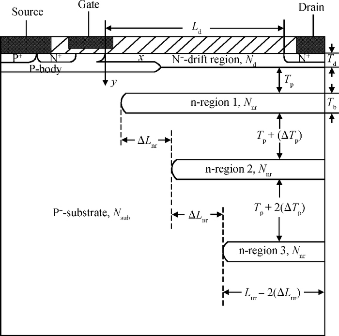
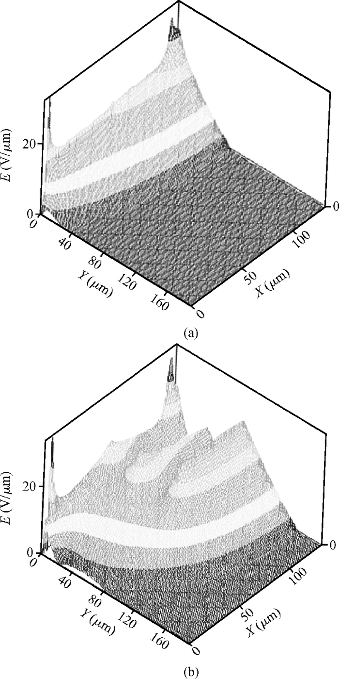
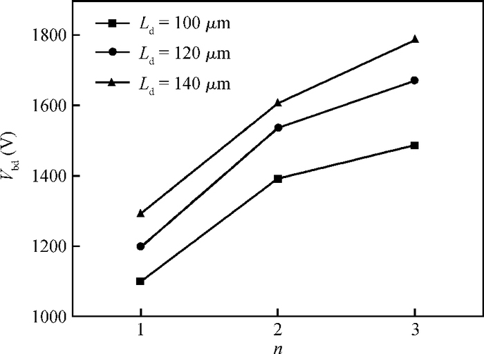
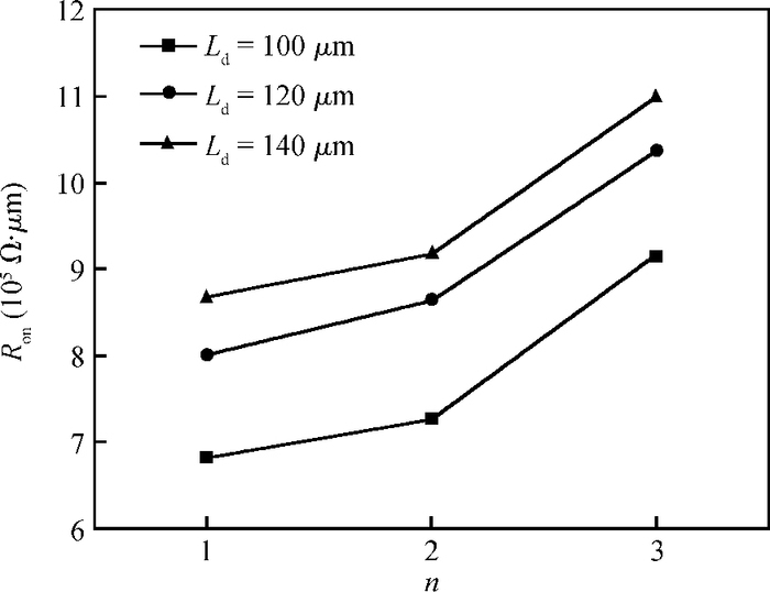
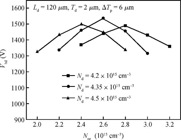
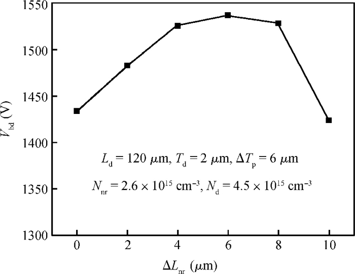
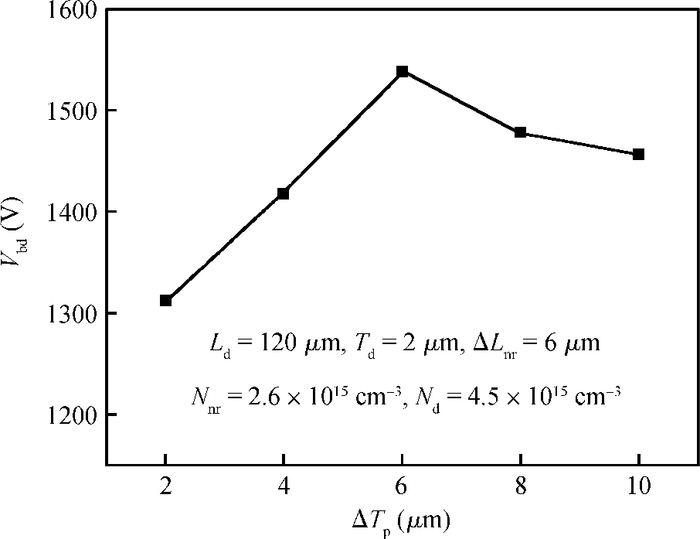
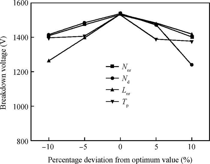
A lateral double-diffused metal-oxide-semiconductor field effect transistor (LDMOST) with multiple n-regions in the p-substrate is investigated in detail. Because of the decrescent n-regions, the electric field distribution is higher and more uniform, and the breakdown voltage of the new structure is increased by 95%, in comparison with that of a conventional counterpart without substrate n-regions. Based on the trade-off between the breakdown voltage and the on-resistance, the optimal number of n-regions and the other key parameters are achieved. Furthermore, sensitivity research shows that the breakdown voltage is relatively sensitive to the drift region doping and the n-regions' lengths.

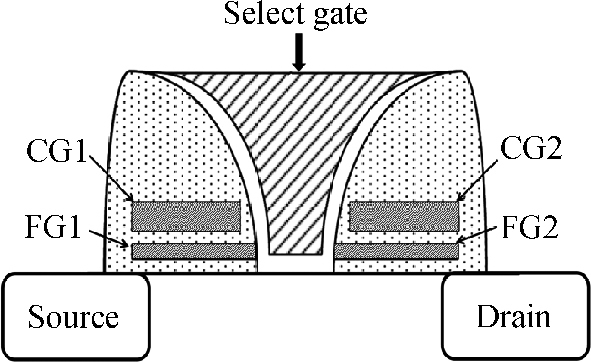
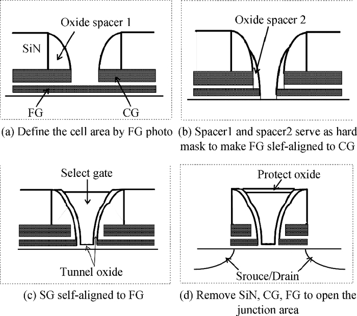
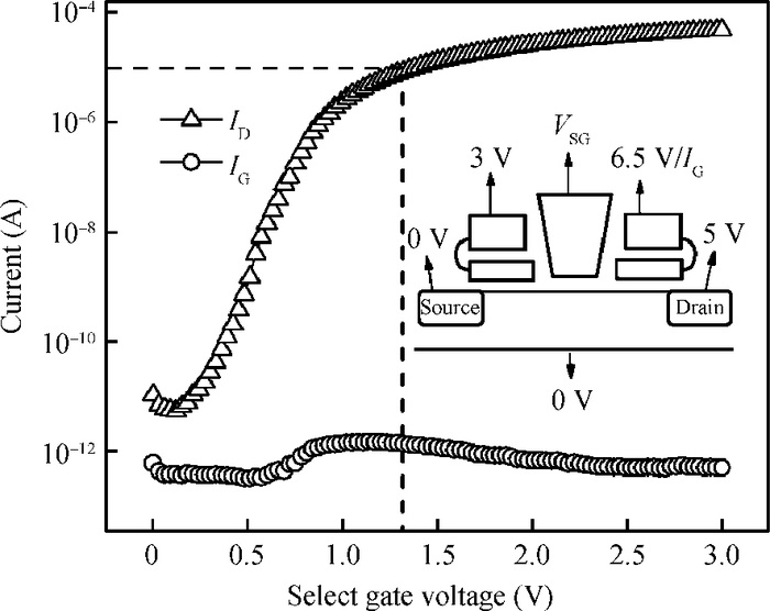
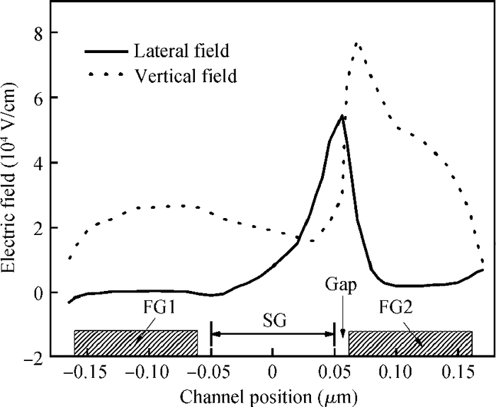
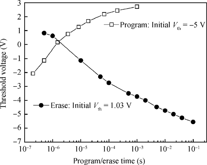
A fully self-aligned symmetrical split-gate cell structure for 2-bit per cell flash memory with a very competitive bit size is presented. One common select gate is located between two floating gates and a pair of source/drain junctions are shared by the 2 bits. The fabrication method utilized here to create a self-aligned structure is to form a spacer against the prior layer without any additional mask. Although the cell consists of three channels in a series, the attributes from conventional split gate flash are still preserved with appropriate bias conditions. Program and erase operation is performed by using a source side injection (SSI) and a poly-to-poly tunneling mechanism respectively.


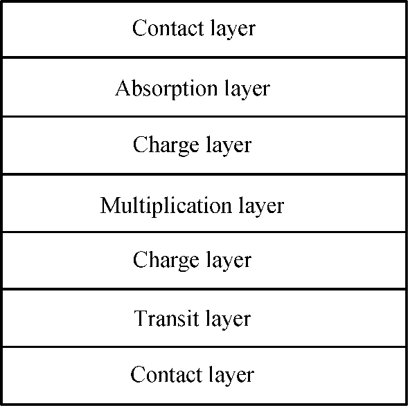
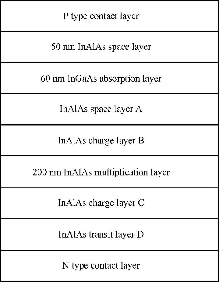
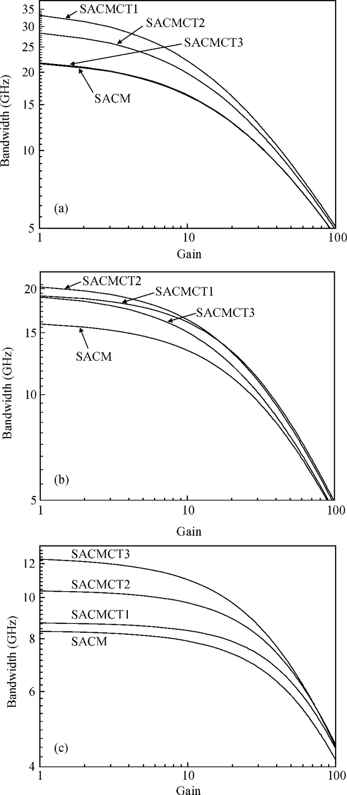
High-speed avalanche photodiodes are widely used in optical communication systems. Nowadays, separate absorption charge and multiplication structure is widely adopted. In this article, a structure with higher speed than separate absorption charge and multiplication structure is reported. Besides the traditional absorption layer, charge layer and multiplication layer, this structure introduces an additional charge layer and transit layer and thus can be referred to as separate absorption, charge, multiplication, charge and transit structure. The introduction of the new charge layer and transit layer brings additional freedom in device structure design. The benefit of this structure is that the carrier transit time and device capacitance can be reduced independently, thus the 3 dB bandwidth could be improved by more than 50% in contrast to the separate absorption charge and multiplication structure with the same size.

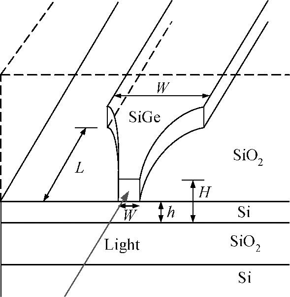
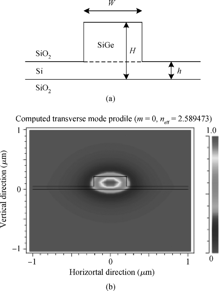
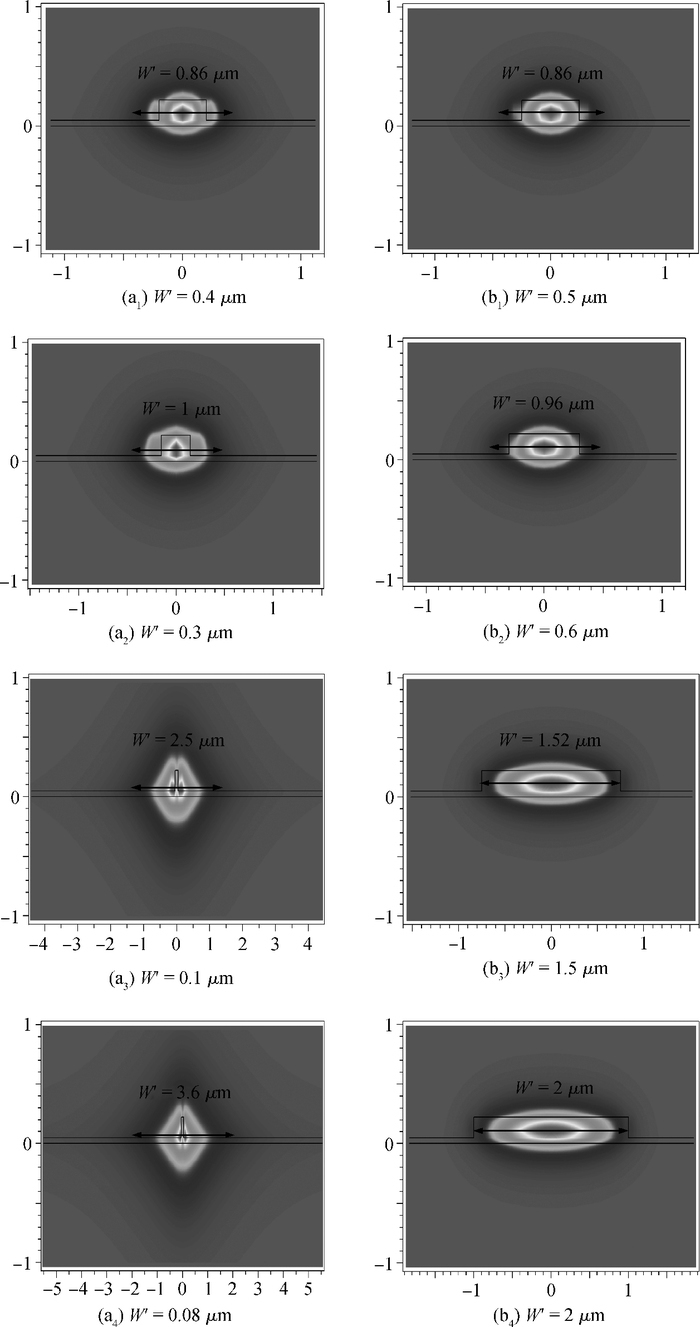
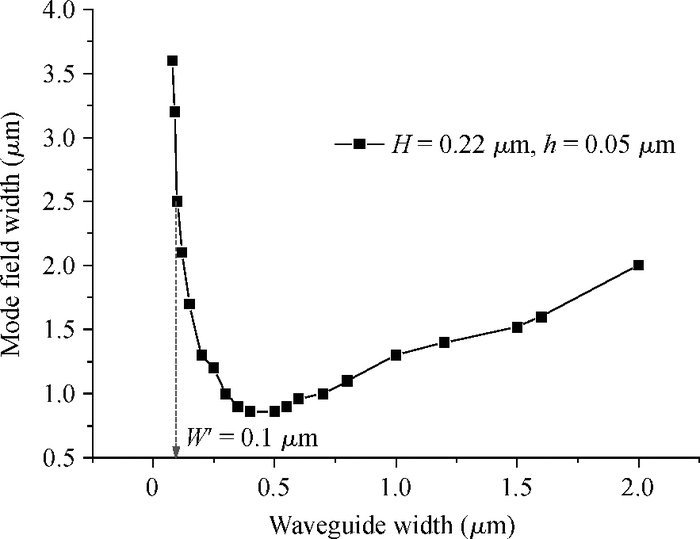
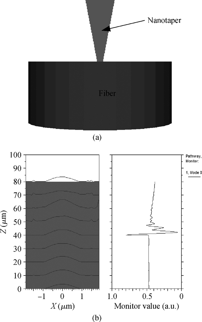
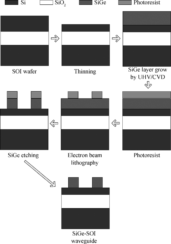
Based on a submicrometer-sized SiGe-SOI waveguide, the coupling loss mechanism is analyzed between the submicrometer-sized SiGe-SOI waveguide and the fiber. The main sources of coupling loss are analyzed, and the mismatch loss of the mode field is the mainly lost during connection between the submicrometer-sized waveguide and the fiber. In order to reduce the mismatch loss of the mode field, the structure of a nanotaper SiGe-SOI waveguide with a nanometer-sized tip is adopted. By reducing the waveguide dimensions to increase the mode field size, coupling loss could be reduced between the waveguide and the fiber. Different mode field dimensions of nanotaper SiGe-SOI waveguides and fiber are quantitatively analyzed, and the quantitative relationship between nanotaper SiGe-SOI waveguide dimensions and mode field dimensions are obtained. Finally, nanotaper SiGe-SOI waveguides are made, and the test and analysis have been done. The final experimental results accord well with the theoretical analysis. When the waveguide width is 0.5 μm, the minimum coupling loss of the SiGe-SOI waveguide is 0.56 dB/facet, and also the correctness of the design method and theoretical analysis are verified.


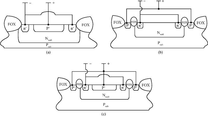
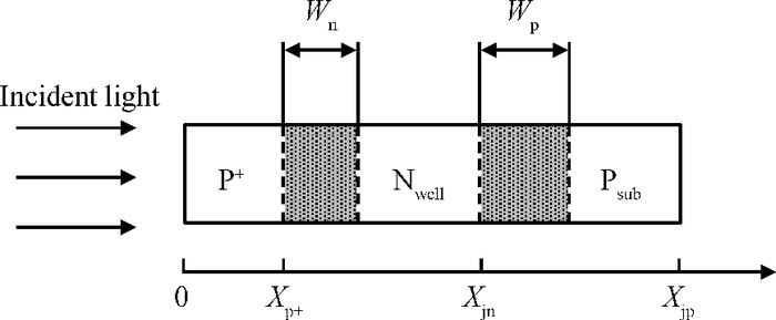
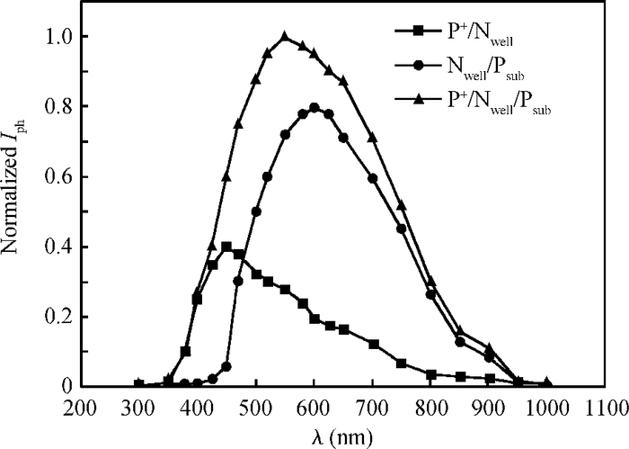
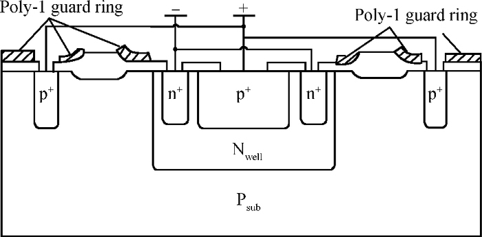
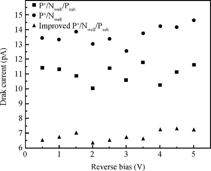
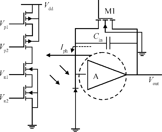
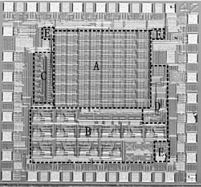
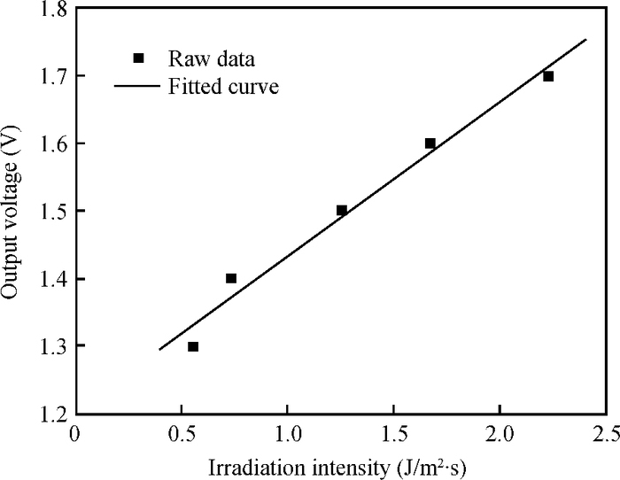
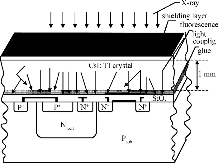
A CMOS compatible P+/Nwell/Psub double junction photodiode pixel was proposed, which can efficiently detect fluorescence from CsI(Tl) scintillation in an X-ray sensor. Photoelectric and spectral responses of P+/Nwell, Nwell/Psub and P+/Nwell/Psub photodiodes were analyzed and modeled. Simulation results show P+/Nwell/Psub photodiode has larger photocurrent than P+/Nwell photodiode and Nwell/Psub photodiode, and its spectral response is more in accordance with CsI(Tl) fluorescence spectrum. Improved P+/Nwell/Psub photodiode detecting CsI(Tl) fluorescence was designed in CSMC 0.5 μm CMOS process, CTIA (capacitive transimpedance amplifier) architecture was used to readout photocurrent signal. CMOS X-ray sensor IC prototype contains 8×8 pixel array and pixel pitch is 100×100 μm2. Testing results show the dark current of the improved P+/Nwell/Psub photodiode (6.5 pA) is less than that of P+/Nwell and P+/Nwell/Psub photodiodes (13 pA and 11 pA respectively). The sensitivity of P+/Nwell/Psub photodiode is about 20 pA/lux under white LED. The spectrum response of P+/Nwell/Psub photodiode ranges from 400 nm to 800 nm with a peak at 532 nm, which is in accordance with the fluorescence spectrum of CsI(Tl) in an indirect X-ray sensor. Preliminary testing results show the sensitivity of X-ray sensor IC under Cu target X-ray is about 0.21 V·m2/W or 5097e-/pixel@8.05 keV considering the pixel size, integration time and average energy of X-ray photons.


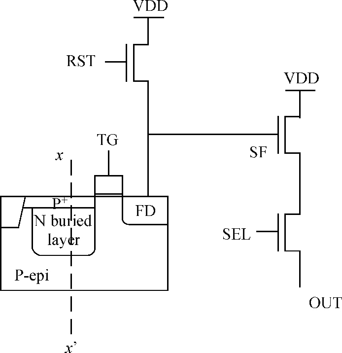
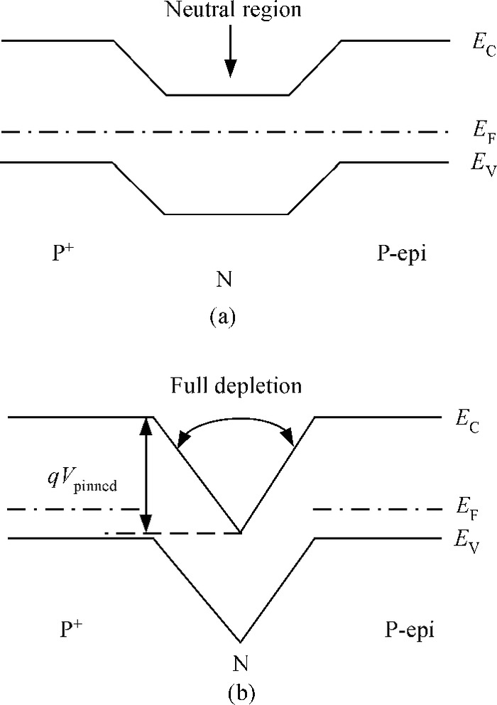
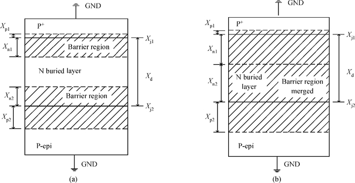
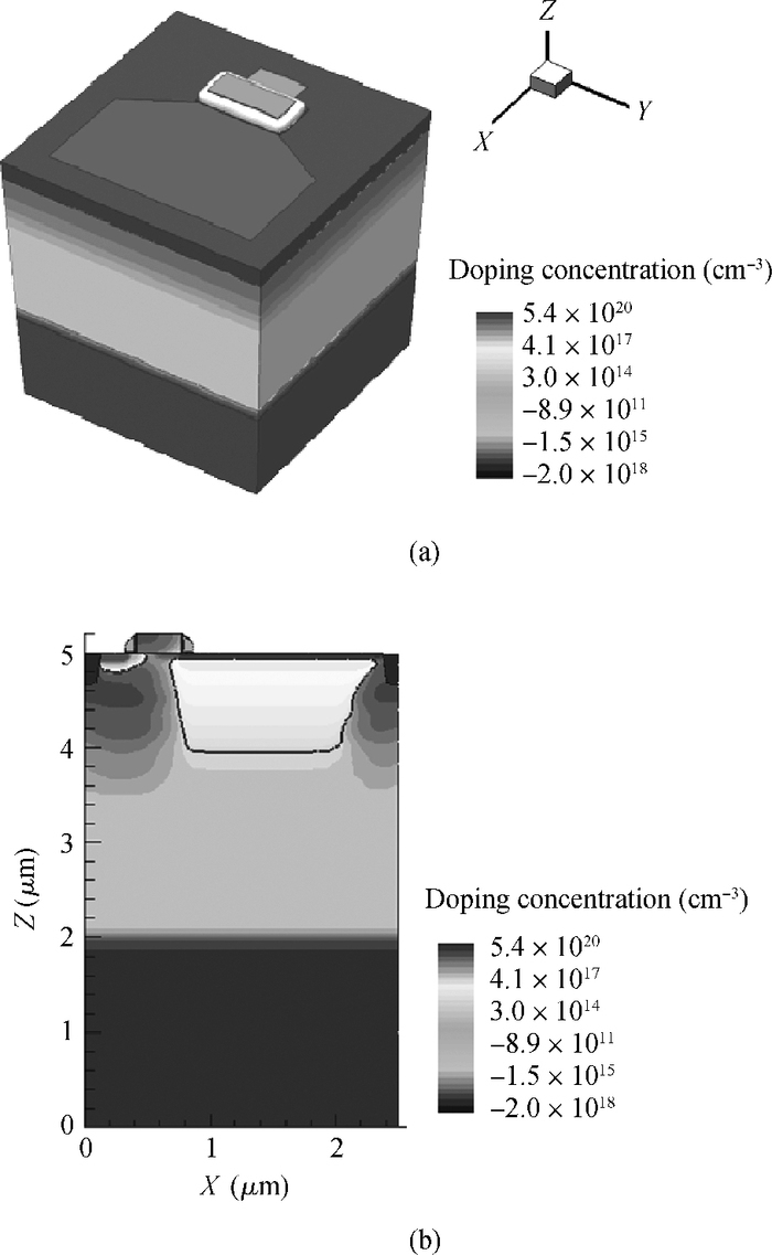
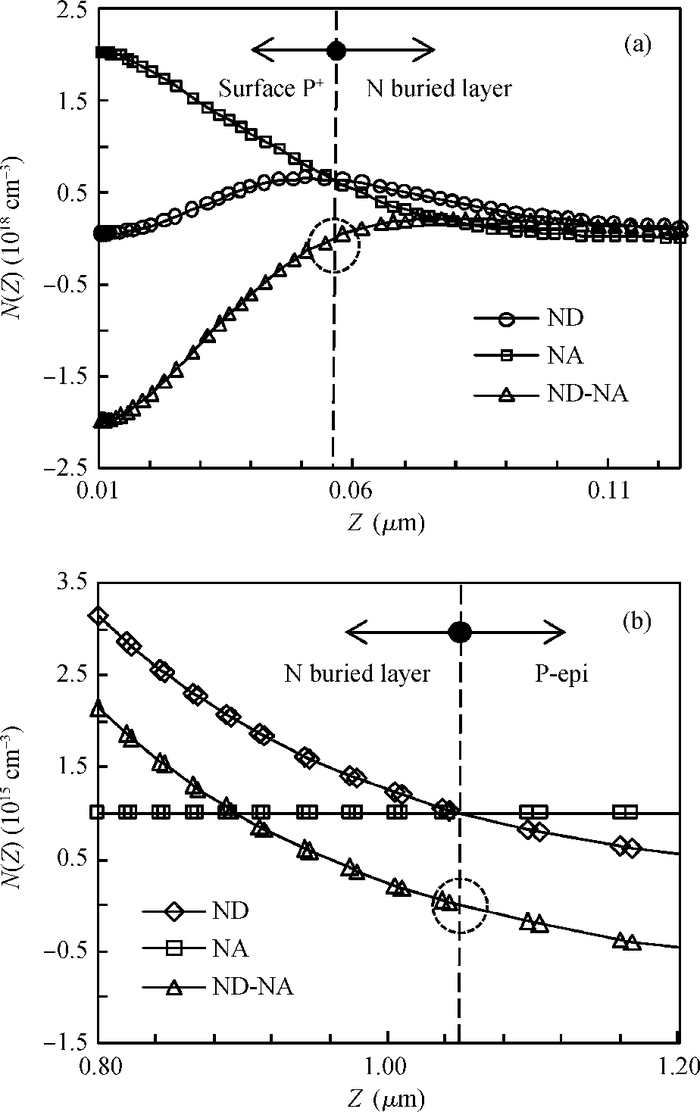
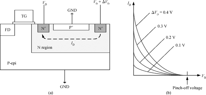
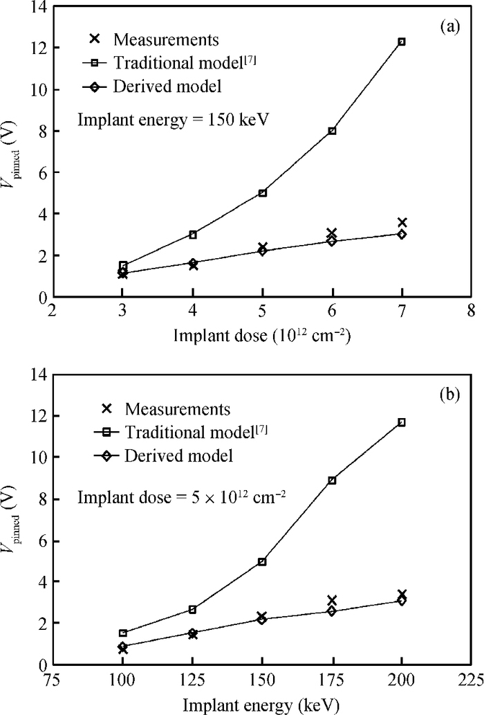
A novel analytical model of pinch-off voltage for CMOS image pixels with a pinned photodiode structure is proposed. The derived model takes account of the gradient doping distributions in the N buried layer due to the impurity compensation formed by manufacturing processes; the impurity distribution characteristics of two boundary PN junctions located in the region for particular spectrum response of a pinned photodiode are quantitative analyzed. By solving Poisson's equation in vertical barrier regions, the relationships between the pinch-off voltage and the corresponding process parameters such as peak doping concentration, N type width and doping concentration gradient of the N buried layer are established. Test results have shown that the derived model features the variations of the pinch-off voltage versus the process implant conditions more accurately than the traditional model. The research conclusions in this paper provide theoretical evidence for evaluating the pinch-off voltage design.

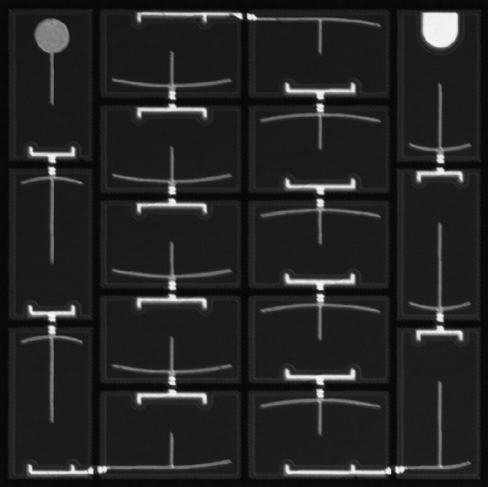
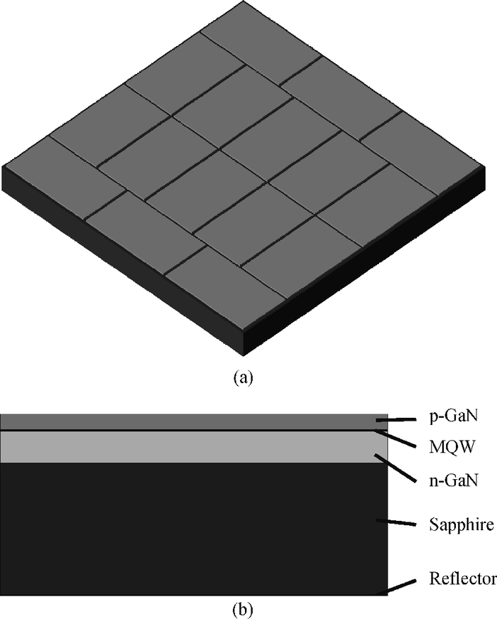
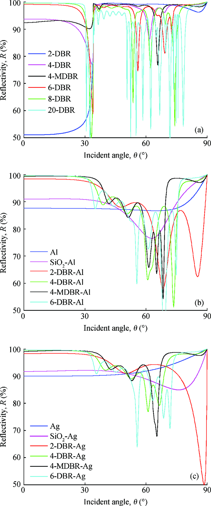
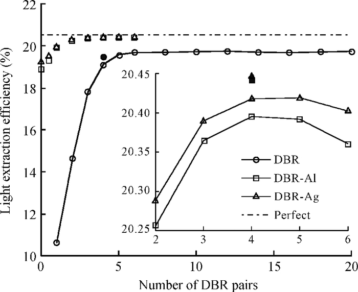
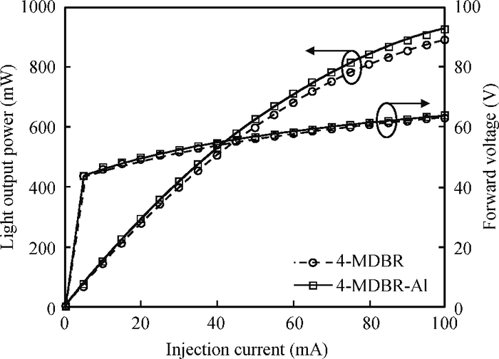
High-voltage light-emitting diodes with backside reflector, including Ti3O5/SiO2 distributed Bragg reflector (DBR) or hybrid reflector combining DBR and Al or Ag metal layer, are investigated using Monte Carlo ray tracing method. The hybrid reflector leads to more enhancement of light-extraction efficiency (LEE). Moreover, the LEE can also be improved by redesigning the thicknesses of DBR. HV-LED with four redesigned DBR pairs (4-MDBR), and those with a hybrid reflector combining 4-MDBR and Al metal layer (4-MDBR-Al), are fabricated. Compared to 4-MDBR, the enhancement of light-output power induced by 4-MDBR-Al is 4.6%, which is consistent with the simulated value of 4.9%.
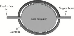
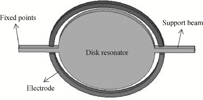
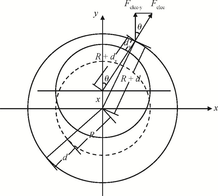
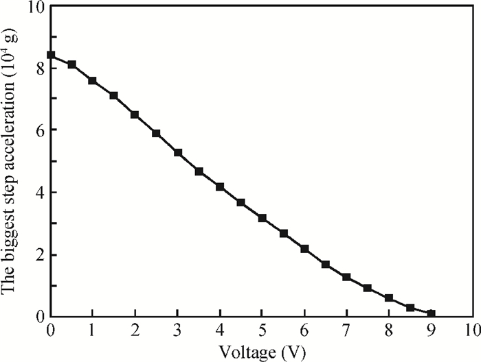
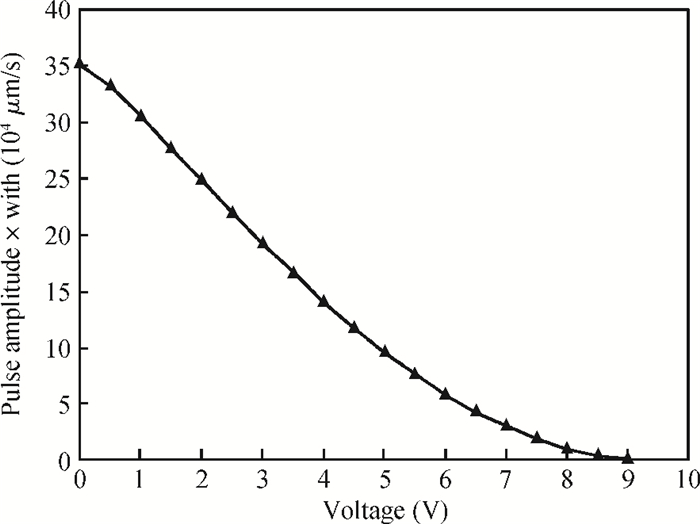
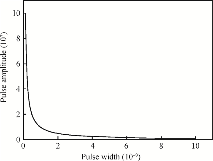
Increasing the bias voltage is a method of reducing the motional resistance of the capacitive disk resonator to match the impedance of the RF circuit. But there are few reports on the study of reliable working range of bias voltage under the shock and vibration environment. Therefore, the reliability of disk resonator under the step and pulse acceleration impact respectively is systematically analyzed in this paper. By the expression of the biggest inertial acceleration the disk can bear under the reliable condition, the maximal reliable range curves of the disk resonator under the dynamic impact environment are obtained. According to the actual sizes of disk in the literature, it can be seen that when a step shock of 13000 g is supplied, the reliability range is reduced to 75% compared with the original state. For the pulse shock, the reliability range is related to the pulse amplitude and time width. Research of this paper can provide the basis for the selection of bias voltage of disk resonator under the inertial shock.
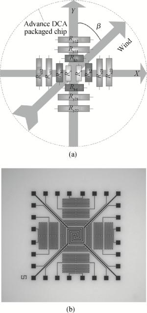
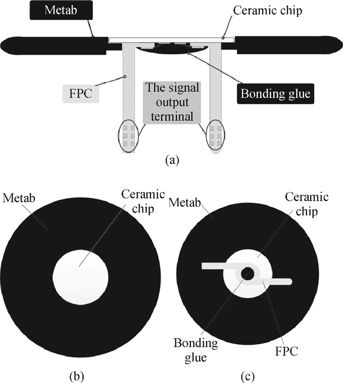
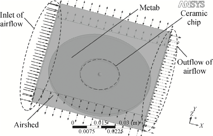
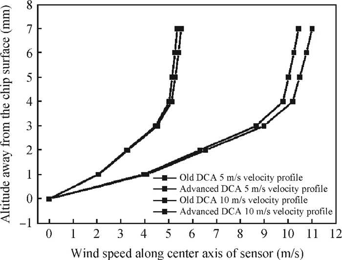
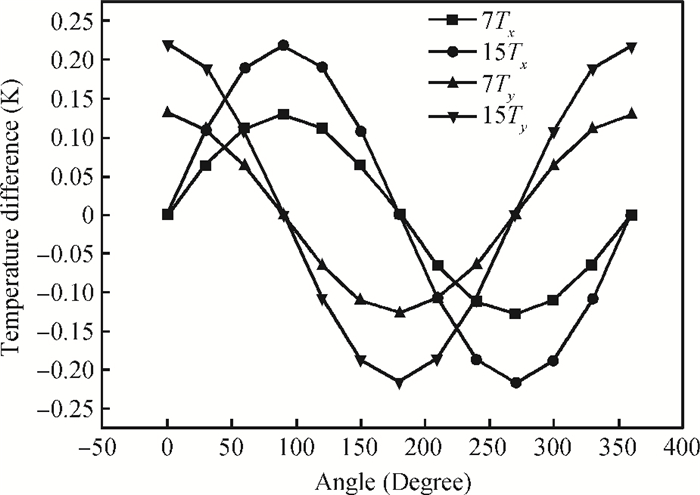
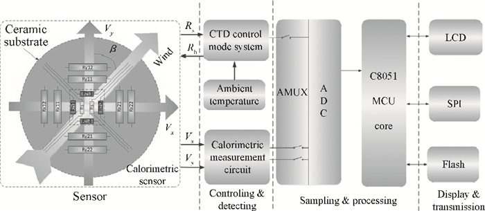
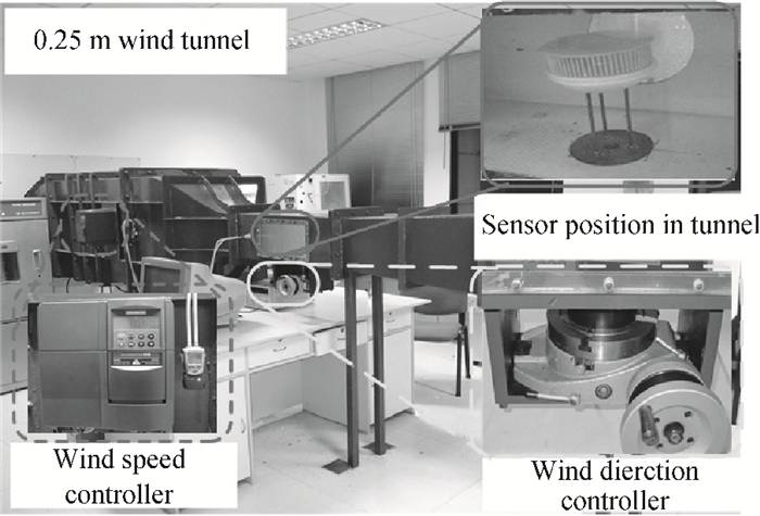
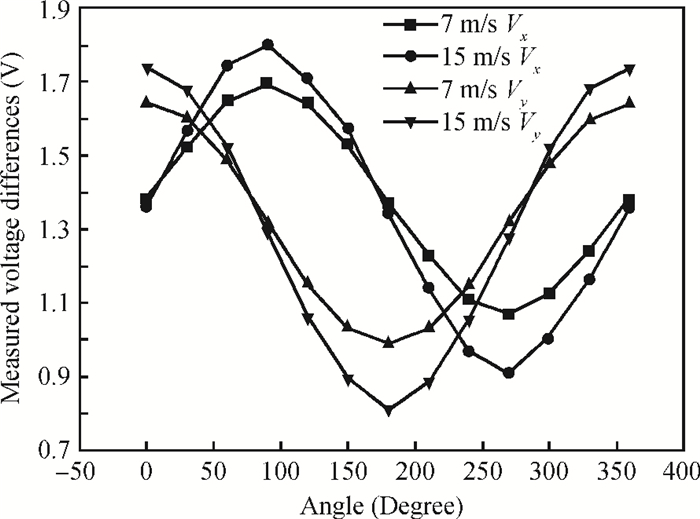
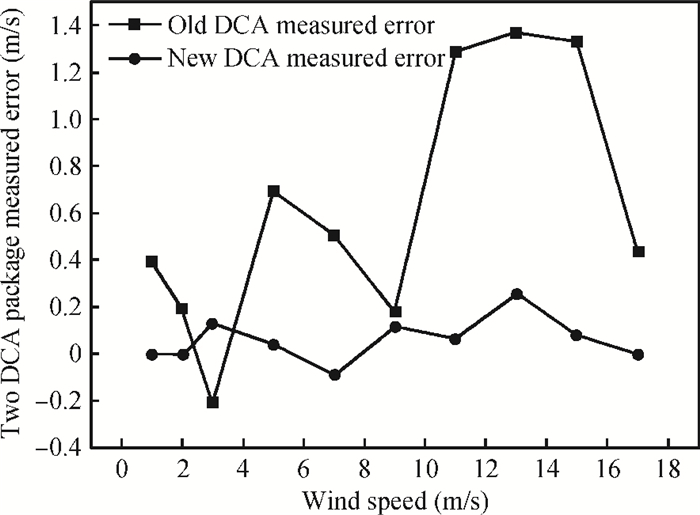
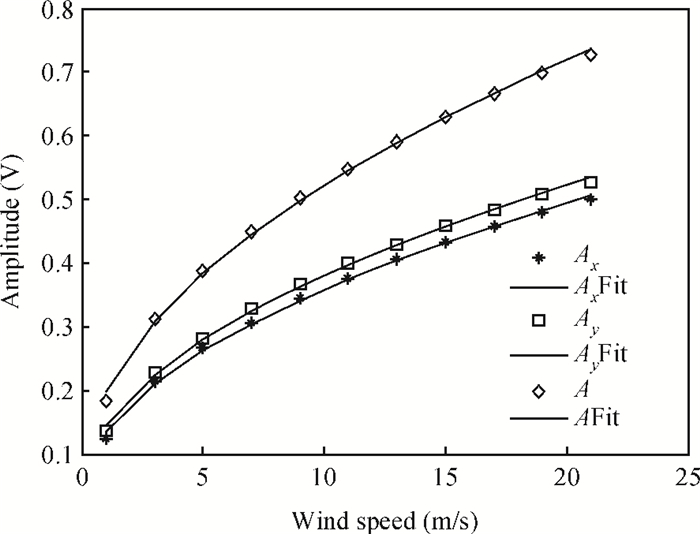
An advanced direct chip attach packaged two-dimensional ceramic thermal wind sensor is studied. The thermal wind sensor chip is fabricated by metal lift-off processes on the ceramic substrate. An advanced direct chip attach (DCA) packaging is adopted and this new packaged method simplifies the processes of packaging further. Simulations of the advanced DCA packaged sensor based on computational fluid dynamics (CFD) model show the sensor can detect wind speed and direction effectively. The wind tunnel testing results show the advanced DCA packaged sensor can detect the wind direction from 0° to 360° and wind speed from 0 to 20 m/s with the error less than 0.5 m/s. The nonlinear fitting based least square method in Matlab is used to analyze the performance of the sensor.


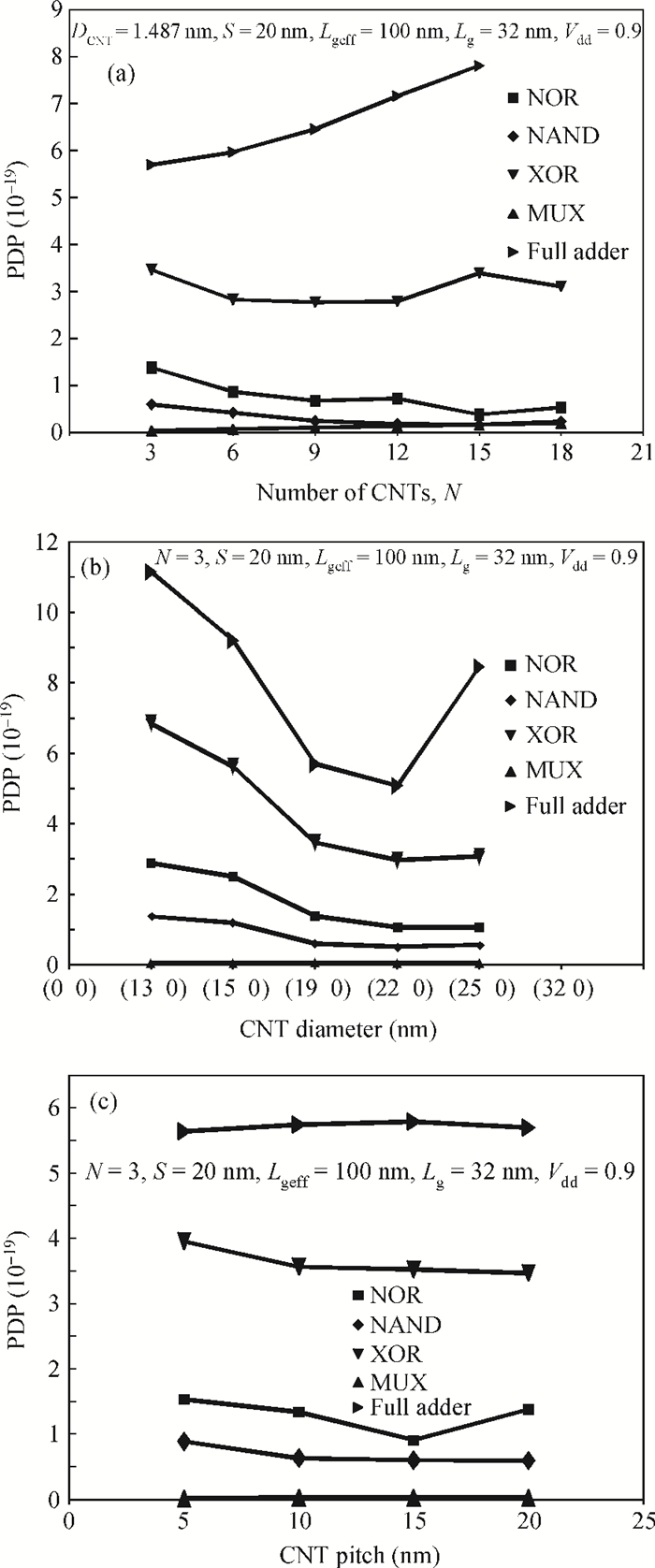
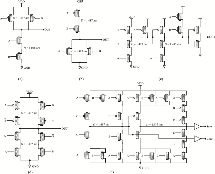
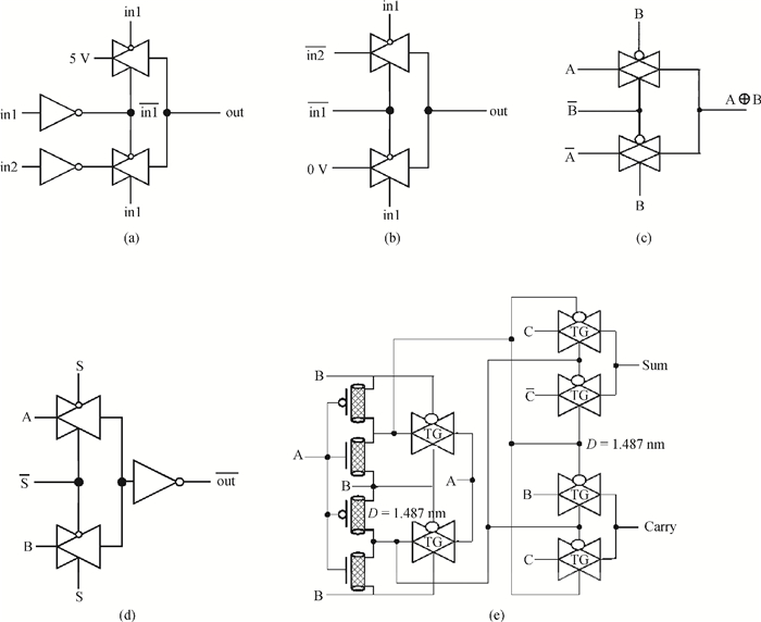
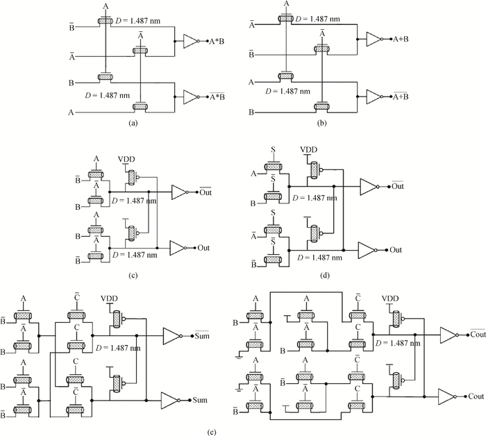
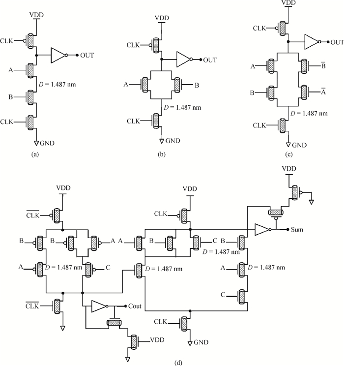
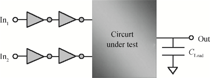
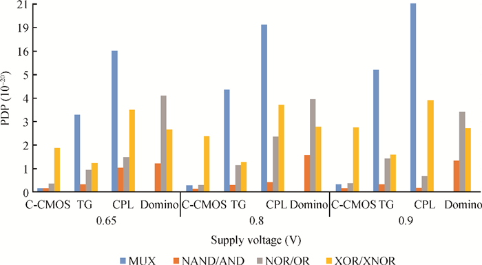
The next generation of logic gate devices are expected to depend upon radically new technologies mainly due to the increasing difficulties and limitations of existing CMOS technology. MOSFET like CNFETs should ideally be the best devices to work with for high-performance VLSI. This paper presents results of a comprehensive comparative study of MOSFET-like carbon nanotube field effect transistors (CNFETs) technology based logic gate library for high-speed, low-power operation than conventional bulk CMOS libraries. It focuses on comparing four promising logic families namely:complementary-CMOS (C-CMOS), transmission gate (TG), complementary pass logic (CPL) and Domino logic (DL) styles are presented. Based on these logic styles, the proposed library of static and dynamic NAND-NOR logic gates, XOR, multiplexer and full adder functions are implemented efficiently and carefully analyzed with a test bench to measure propagation delay and power dissipation as a function of supply voltage. This analysis provides the right choice of logic style for low-power, high-speed applications. Proposed logic gates libraries are simulated using Synopsys HSPICE based on the standard 32 nm CNFET model. The simulation results demonstrate that, it is best to use C-CMOS logic style gates that are implemented in CNFET technology which are superior in performance compared to other logic styles, because of their low average power-delay-product (PDP). The analysis also demonstrates how the optimum supply voltage varies with logic styles in ultra-low power systems. The robustness of the proposed logic gate library is also compared with conventional and state-art of CMOS logic gate libraries.

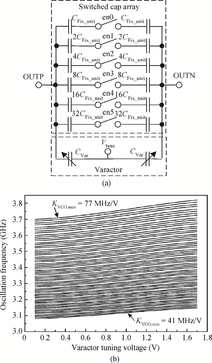
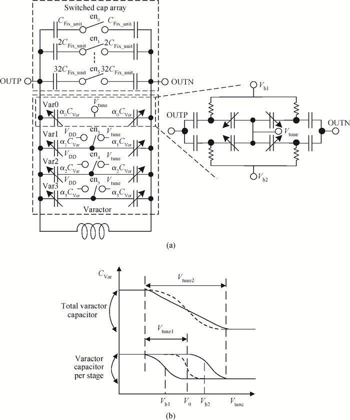
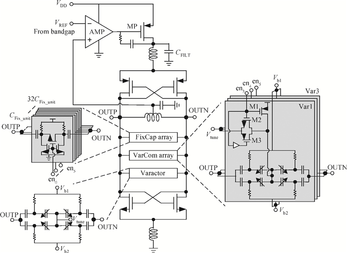
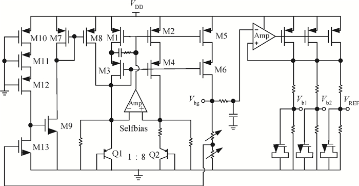
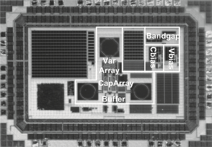
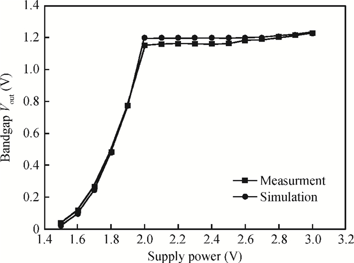
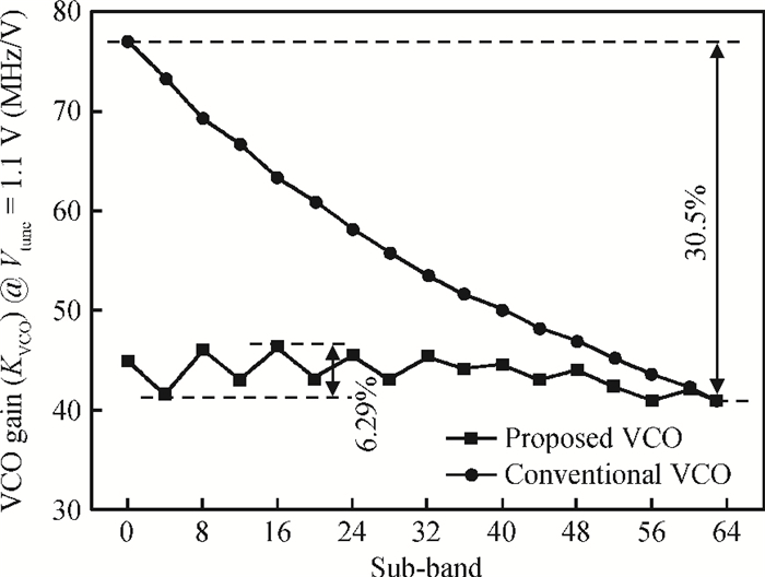
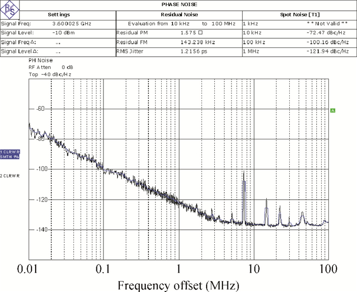
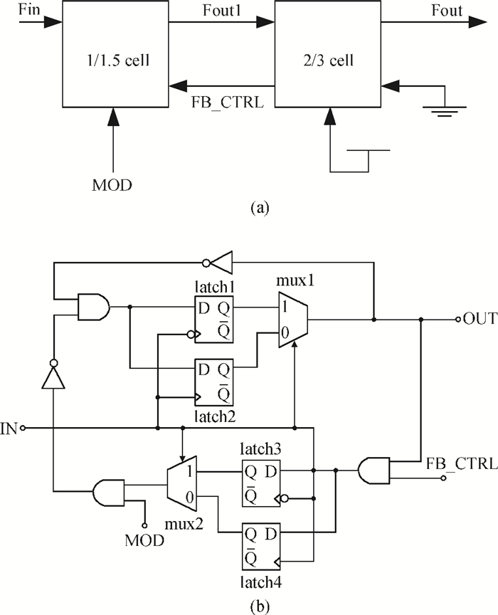
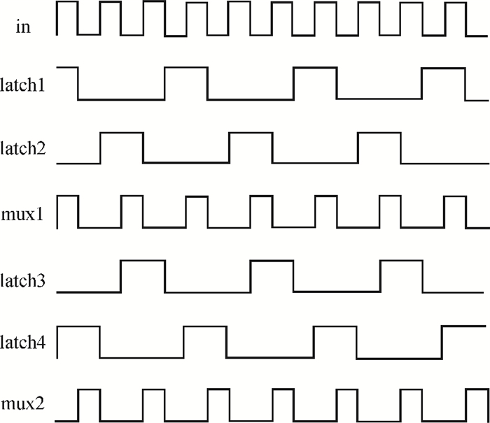
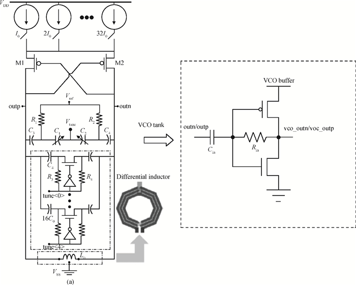
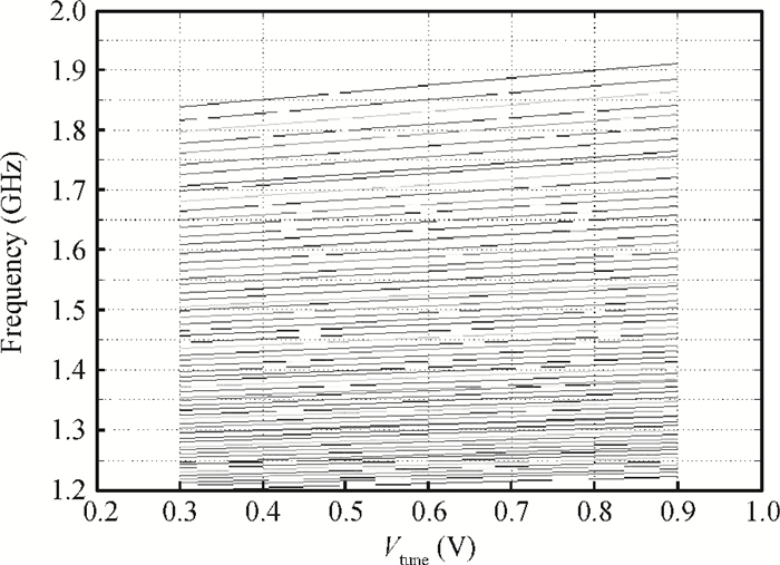
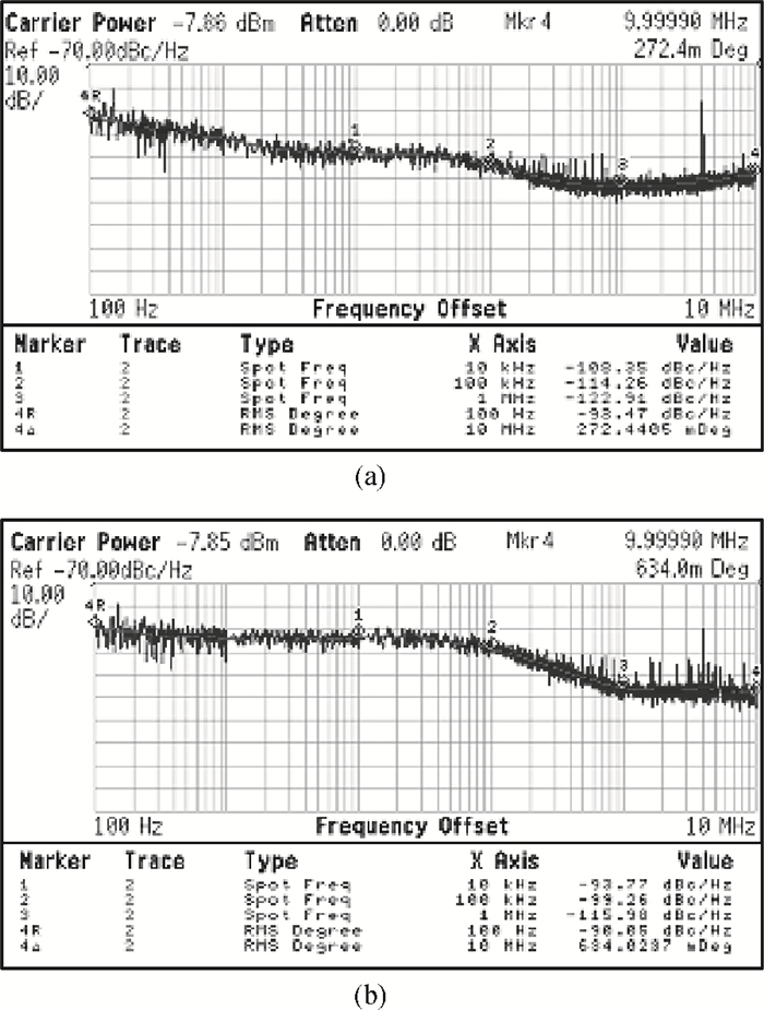
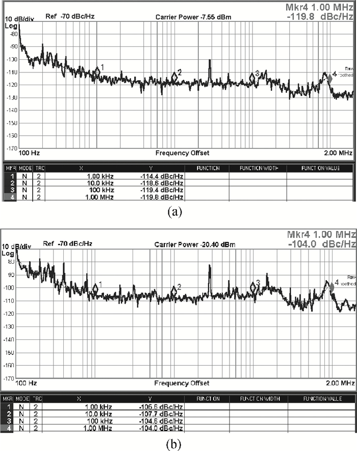
A wideband low-phase-noise LC voltage-controlled oscillator (VCO) with low VCO gain (KVCO) variation for WLAN fractional-N frequency synthesizer application is proposed and designed on a 0.13-μm CMOS process. In order to achieve a low KVCO variation, an extra switched varactor array was added to the LC tank with the conventional switched capacitor array. Based on the proposed switched varactor array compensation technique, the measured KVCO is 43 MHz/V with only 6.29% variation across the entire tuning range. The proposed VCO provides a tuning range of 23.7% from 3.01 to 3.82 GHz, while consuming 9 mA of quiescent current from a 2.3 V supply. The VCO shows a low phase noise of -121.94 dBc/Hz at 1 MHz offset, from the 3.6 GHz carrier.
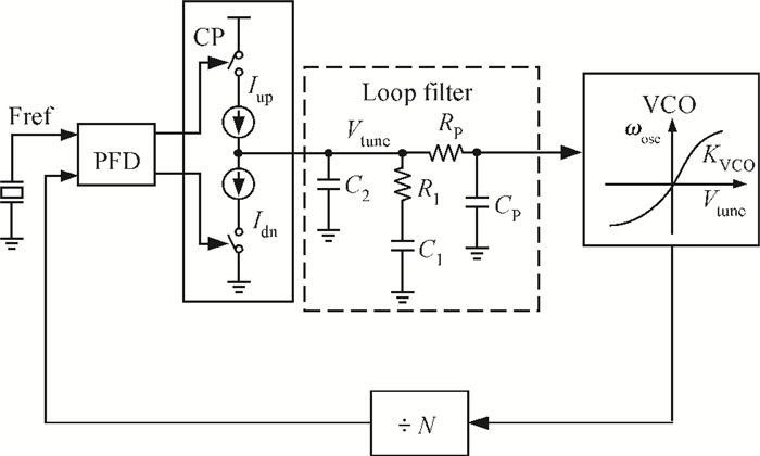

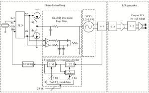
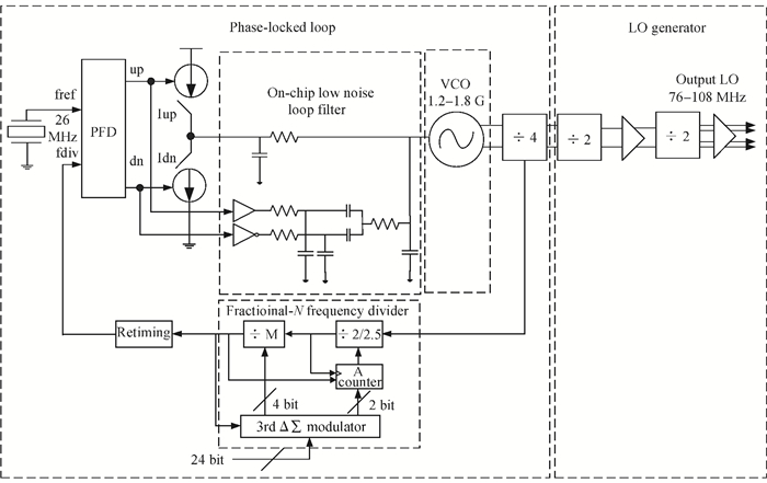
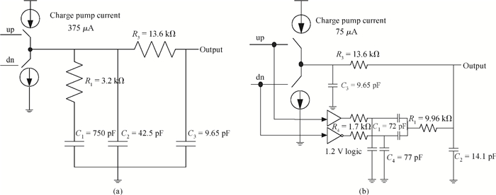
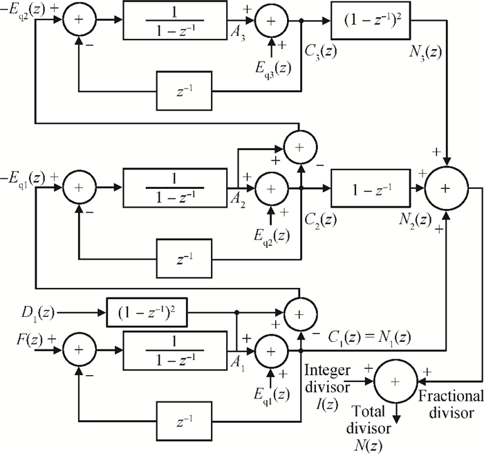
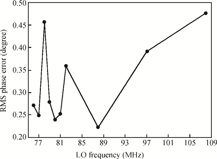
A Δ Σ fractional-N frequency synthesizer fabricated in a 130 nm CMOS technology is presented for the application of an FM tuner. A low noise filter, occupying a small die area and decreasing the output noise, is integrated on a chip. A quantization noise suppression technique, using a reduced step size of the frequency divider, is also adopted. The proposed synthesizer needs no off-chip components and occupies an area of 0.7 mm2. The in-band phase noise (from 10 to 100 kHz) below -108 dBc/Hz and out-of-band phase noise of -122.9 dBc/Hz (at 1 MHz offset) are measured with a loop bandwidth of 200 kHz. The quantization noise suppression technique reduces the in-band and out-of band phase noise by 15 dB and 7 dB respectively. The integrated RMS phase error is no more than 0.48°. The proposed synthesizer consumes a total power of 7.4 mW and the frequency resolution is less than 1 Hz.

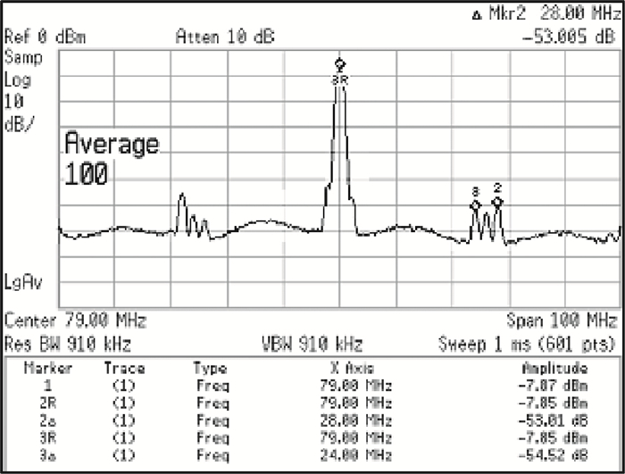
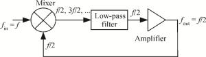
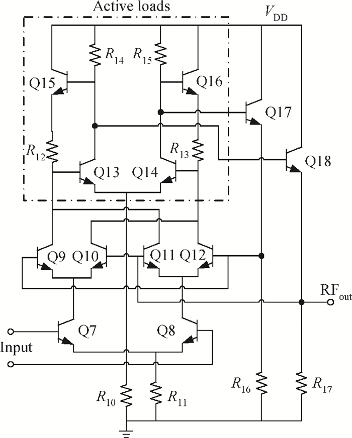
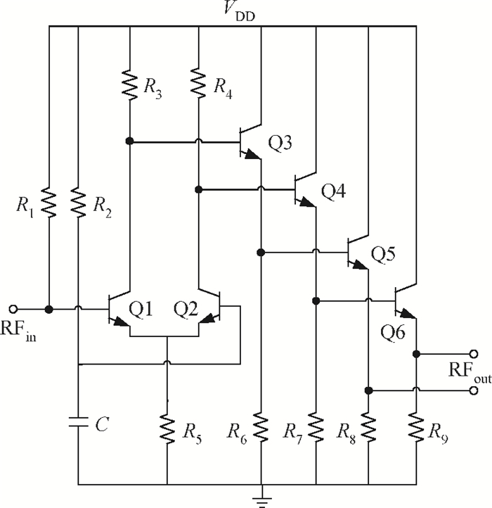
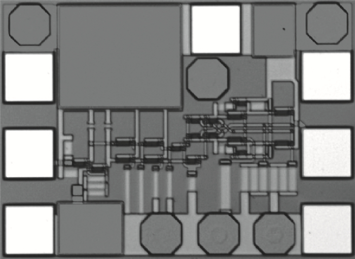
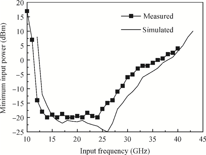
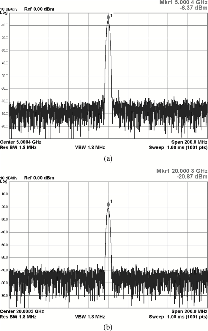
A dynamic divide-by-two regenerative frequency divider (RFD) is presented in a 60-GHz-fT InGaP/GaAs heterojunction bipolar transistors (HBTs) technology. To achieve high operation bandwidth, active loads instead of resistor loads are incorporated into the RFD. On-wafer measurement shows that the divider is operating from 10 GHz up to at least 40 GHz, limited by the available input frequency. The maximum operation frequency of the divider is found to be much higher than fT/2 of the transistor, and also the divider has excellent input sensitivity. The divider consumes 300.85 mW from 5 V supply and occupies an area of 0.47×0.22 mm2.

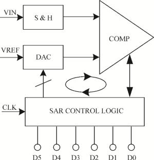
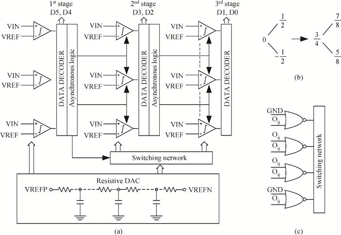
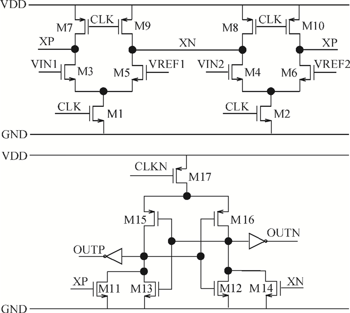
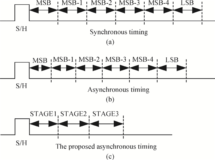
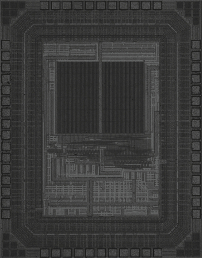
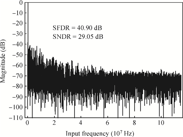
This paper proposes a single channel, 6-bit 230-MS/s asynchronous successive approximation register analog-to-digital converter (ADC) in an SMIC 65 nm CMOS technology. Through adopting the modified 2 bits/stage asynchronous control logic, the presented ADC actualizes a peak 40.90-dB spurious-free dynamic range and 29.05-dB signal-to-noise and distortion ratio at 230-MS/s sampling rate. Utilizing the dynamic comparator without the preamplifier, this work attains low-power design with only 0.93 mW power consumption and accomplishes a figure of merit of 174.67 fJ/step at 1 V supply voltage.


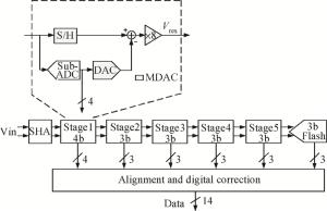
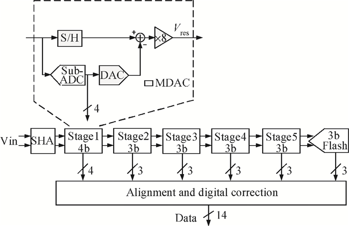
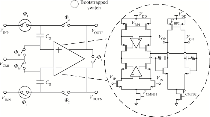
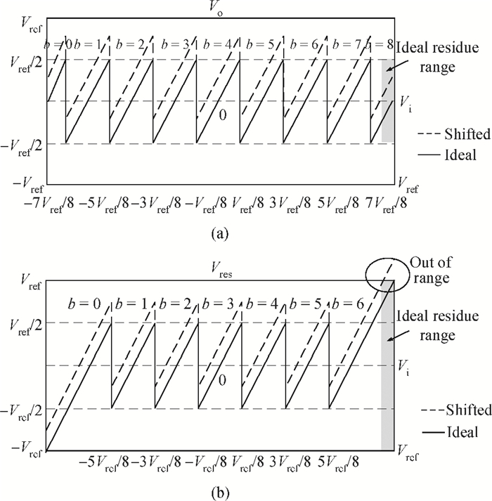
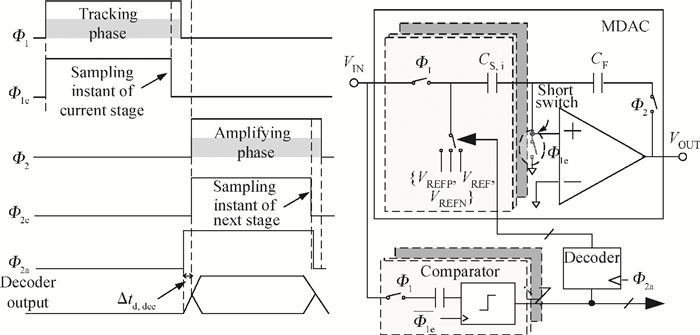
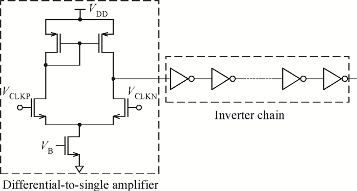
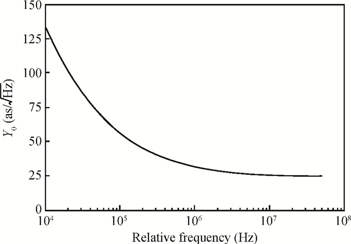
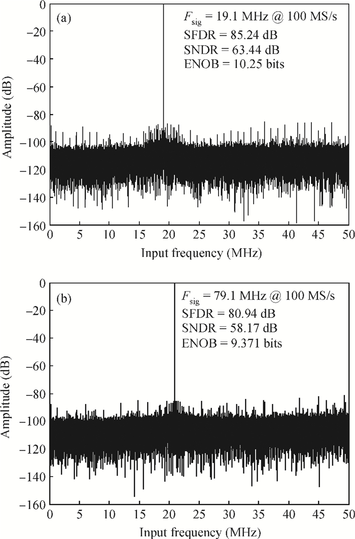
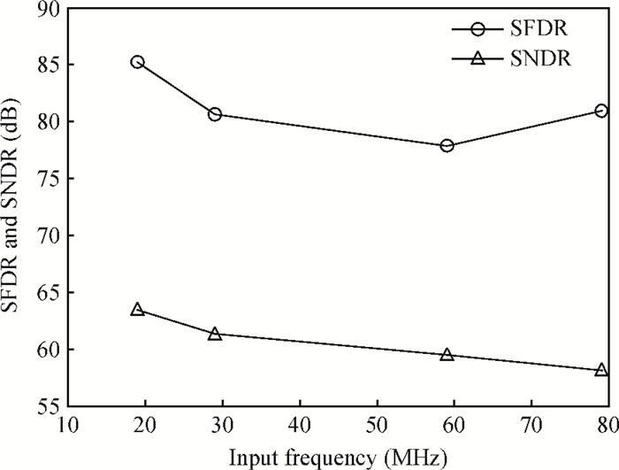
This paper describes a 14-bit 100-MS/s calibration-free pipelined analog-to-digital converter (ADC). Choices for stage resolution as well as circuit topology are carefully considered to obtain high linearity without any calibration algorithm. An adjusted timing diagram with an additional clock phase is proposed to give residue voltage more settling time and minimize its distortion. The ADC employs an LVDS clock input buffer with low-jitter consideration to ensure good performance at high sampling rate. Implemented in a 0.18-μm CMOS technology, the ADC prototype achieves a spurious free dynamic range (SFDR) of 85.2 dB and signal-to-noise-and-distortion ratio (SNDR) of 63.4 dB with a 19.1-MHz input signal, while consuming 412-mW power at 2.0-V supply and occupying an area of 2.9×3.7 mm2.


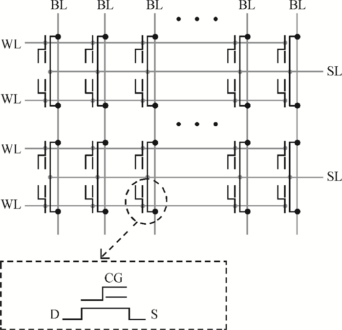
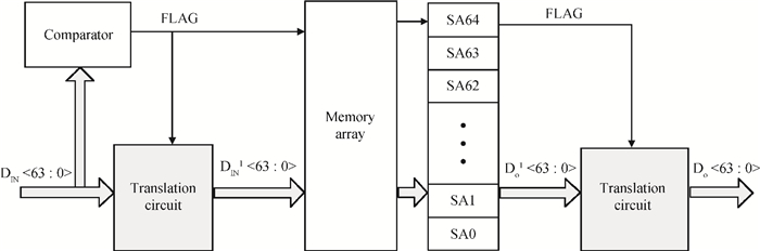
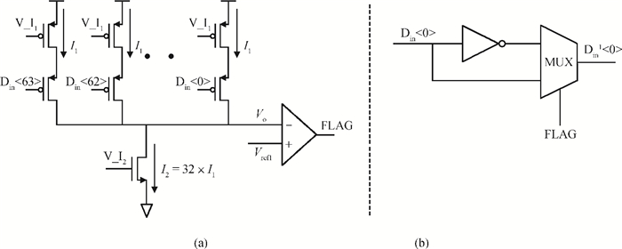
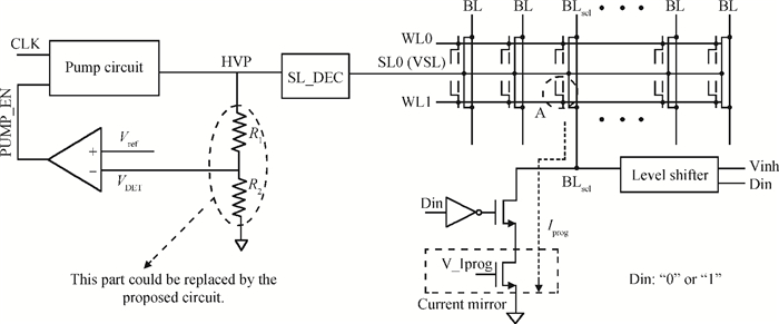
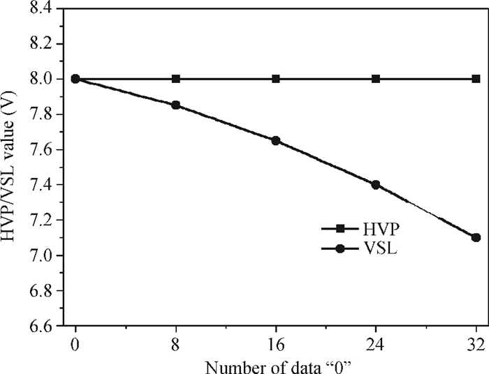
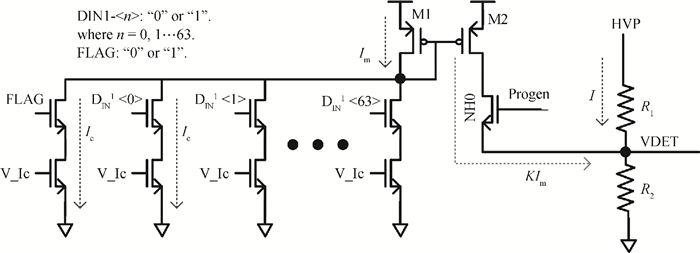
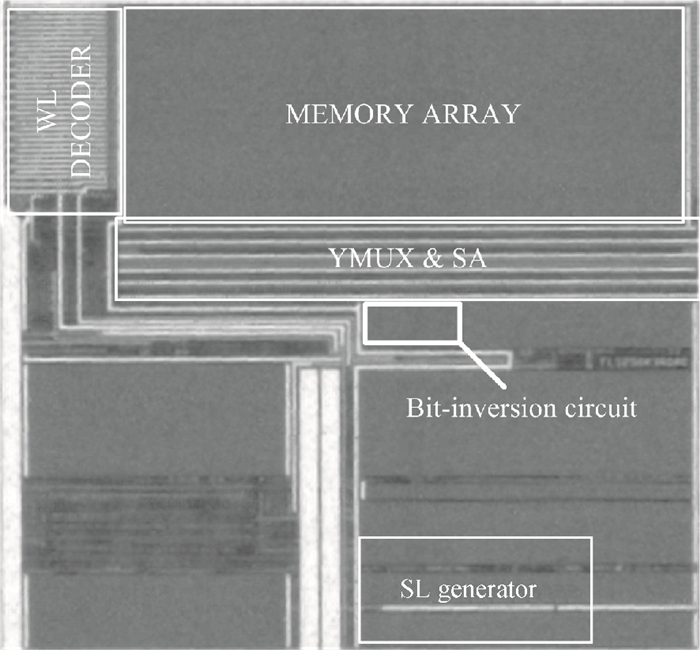
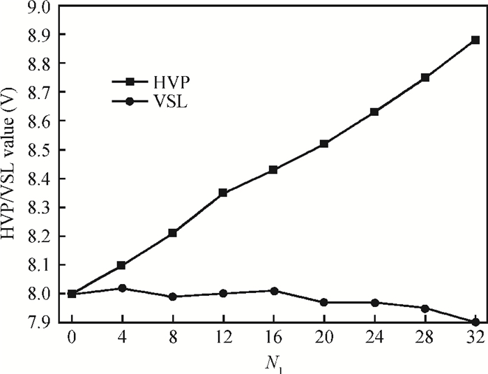
A novel sourceline voltage compensation circuit for program operation in embedded flash memory is presented. With the sourceline voltage compensation circuit, the charge pump can modulate the output voltage according to the number of cells to be programmed with data "0". So the IR drop on the sourceline decoding path is compensated, and a stable sourceline voltage can be obtained. In order to reduce the power dissipation in program operation, a bit-inversion program circuit is adopted. By using the bit-inversion program circuit, the cells programmed to data "0" are limited to half of the bits of a write data word, thus power dissipation in program operation is greatly reduced. A 1.8-V 8×64-kbits embedded NOR flash memory employing the two circuits has been integrated using a GSMC 0.18-μm 4-poly 4-metal CMOS process.
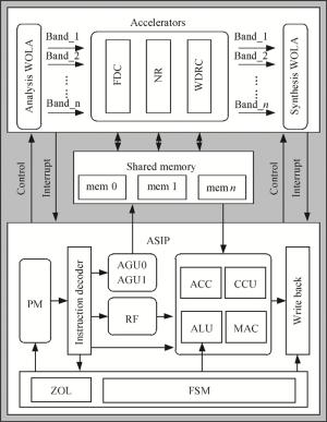
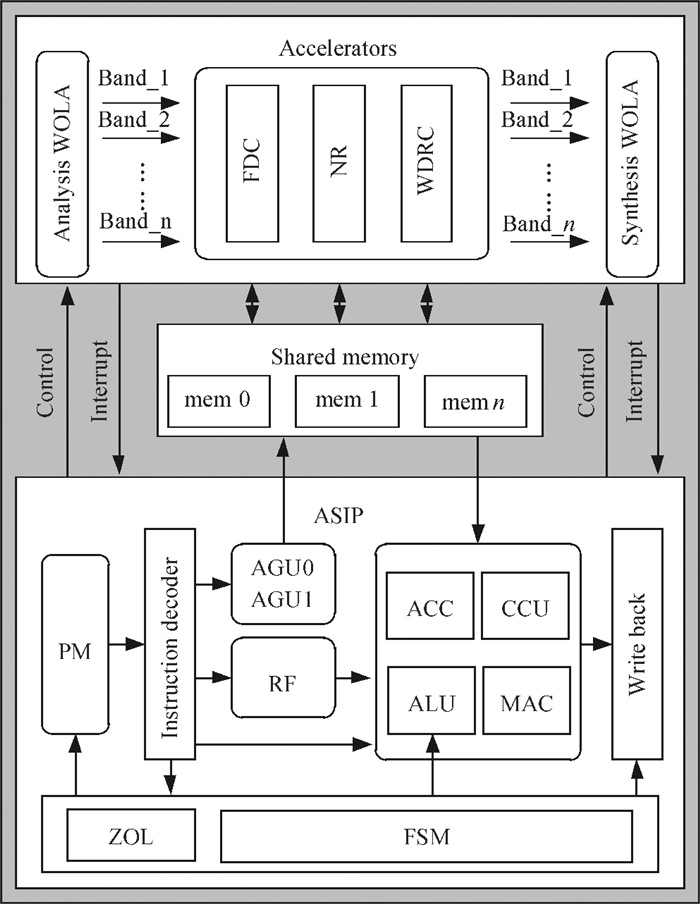
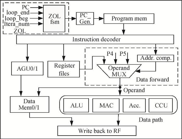
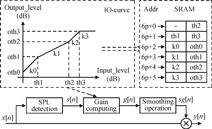
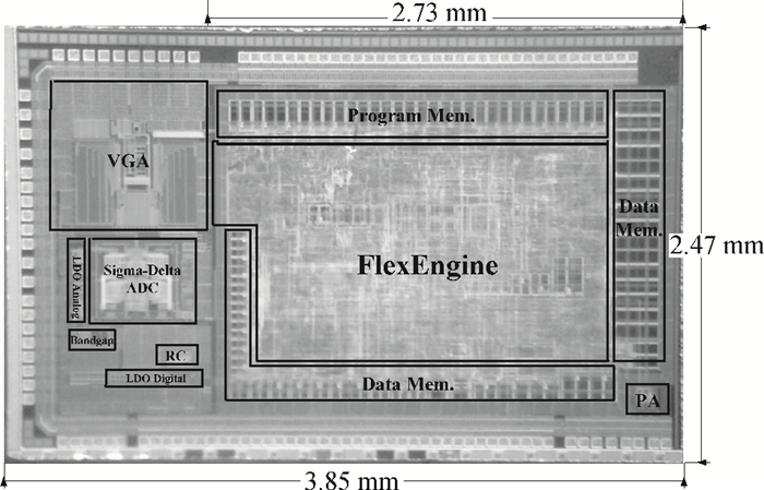
We present a novel audio-processing platform, FlexEngine, which is composed of a 24-bit application-specific instruction-set processor (ASIP) and five dedicated accelerators. Acceleration instructions, compact instructions and repeat instruction are added into the ASIP's instruction set to deal with some core tasks of hearing aid algorithms. The five configurable accelerators are used to execute several of the most common functions of hearing aids. Moreover, several low power strategies, such as clock gating, data isolation, memory partition, bypass mode, sleep mode, are also applied in this platform for power reduction. The proposed platform is implemented in CMOS 130 nm technology, and test results show that power consumption of FlexEngine is 0.863 mW with the clock frequency of 8 MHz at Vdd=1.0 V.