


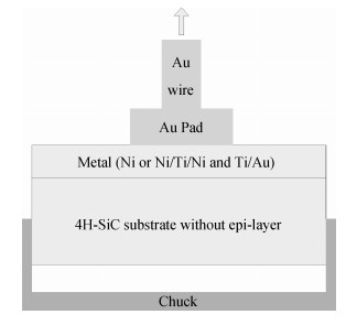
Fig. 1.
Image of the adhesion tests.
SEMICONDUCTOR PHYSICS
Linchao Han1, Huajun Shen1, , Kean Liu2, Yiyu Wang1, Yidan Tang1, Yun Bai1, Hengyu Xu1, Yudong Wu2 and Xinyu Liu1
Corresponding author: Shen Huajun, Email:shenhuajun@ime.ac.cn
Abstract: The Ni/Ti/Ni multilayer ohmic contact properties on a 4H-SiC substrate and improved adhesion with the Ti/Au overlayer have been investigated. The best specific contact resistivity of 3.16×10⁻⁵ Ω·cm2 was obtained at 1050℃. Compared with Ni/SiC ohmic contact, the adhesion between Ni/Ti/Ni/SiC and the Ti/Au overlayer was greatly improved and the physical mechanism under this behavior was analyzed by using Raman spectroscopy and X-ray energy dispersive spectroscopy (EDS) measurement. It is shown that a Ti-carbide and Ni-silicide compound exist at the surface and there is no graphitic carbon at the surface of the Ni/Ti/Ni structure by Raman spectroscopy, while a large amount of graphitic carbon appears at the surface of the Ni/SiC structure, which results in its bad adhesion. Moreover, the interface of the Ni/Ti/Ni/SiC is improved compared to the interface of Ni/SiC.
Keywords: ohmic contact, SiC, Ni/Ti/Ni, Ni2Si
| [1] |
Lu W J, Mitchel W C, Landis G R, et al. Catalytic graphitization and ohmic contact formation on 4H-SiC. J Appl Phys, 2003, 93: 5397 doi: 10.1063/1.1562737
|
| [2] |
Han Ru, Yang Yintang, Wang Ping, et al. Ohmic contact properties of multi-metal film on n-type 4H-SiC. Chinese Journal of Semiconductors, 200728(2): 150 http://en.cnki.com.cn/Article_en/CJFDTOTAL-BDTX200702001.htm
|
| [3] |
Siad M, Abdesslam M, Chami A C. Role of carbon in the formation of ohmic contact in Ni/4H-SiC and Ni/Ti/4H-SiC. Appl Surf Sci, 2012, 258(18): 6819 doi: 10.1016/j.apsusc.2012.03.108
|
| [4] |
Nikitina I P, Vassilevski K V, Wright N G, et al. Formation and role of graphite and nickel silicide in nickel based ohmic contacts to n-type silicon carbide. J Appl Phys, 2005, 97: 5397 http://ieeexplore.ieee.org/xpls/abs_all.jsp?arnumber=5043728
|
| [5] |
Barda B, Machá P, Cicho S, et al. Thermal degradation of Ni-based Schottky contacts on 6H-SiC. Appl Surf Sci, 2011, 257(9): 4418 doi: 10.1016/j.apsusc.2010.12.077
|
| [6] |
Hallin C, Yakimova R, Pécz B, et al. Improved Ni ohmic contact on n-type 4H-SiC. J Electron Mater, 1997, 26: 119 doi: 10.1007/s11664-997-0136-2
|
| [7] |
Marinova T, Kakanakova-Georgieva A, Krastev V, et al. Nickel based ohmic contacts on SiC. Mater Sci Eng B-Solid State Materials for Advanced Technology, 1997, 46: 223 doi: 10.1016/S0921-5107(96)01981-2
|
| [8] |
Zhang Z, Teng J, Yuan W X, et al. Kinetic study of interfacial solid state reactions in the Ni/4H-SiC contact. Appl Surf Sci, 2009, 255: 6939 doi: 10.1016/j.apsusc.2009.03.018
|
| [9] |
Ohyanagi T, Onose Y, Watanabe A. Ti/Ni bilayer ohmic contact on 4H-SiC. J Vac Sci Technol B, 2008, 26: 1359 doi: 10.1116/1.2949116
|
| [10] |
Luckowski E D, Delucca J M, Williams J R, et al. Improved ohmic contact to n-type 4H and 6H-SiC using nichrome. J Electron Mater, 1998, 27: 330 doi: 10.1007/s11664-998-0410-y
|
| [11] |
Guo H, Zhang Y M, Qiao D Y, et al. The fabrication of nickel silicide ohmic contacts to n-type 6H-silicon carbide. Chin Phys, 2007, 16(6): 1753 doi: 10.1088/1009-1963/16/6/046
|
| [12] |
Cho N I, Jung K H, Choi Y. Improved ohmic contact to the n-type 4H-SiC semiconductor using cobalt silicides. Semicond Sci Technol, 2004, 19(3): 306 doi: 10.1088/0268-1242/19/3/003
|
| [13] |
Machá P, Barda B, Kudrnová M. Role of titanium in Ti/Ni ohmic contact on n-type 6H-SiC. Microelectron Eng, 2010, 87: 274 doi: 10.1016/j.mee.2009.06.017
|
| [14] |
Jae Hyun P, Holloway P H. Effects of nickel and titanium thickness on nickel/titanium ohmic contacts to n-type silicon carbide. J Vac Sci Technol B, 2005, 23: 486 doi: 10.1116/1.1868694
|
| [15] |
Wang Shouguo, Zhang Yan, Zhang Yimen, et al. Ohmic contacts of 4H-SiC on ion-implantation layers. Chin Phys B, 2010, 19: 017204 doi: 10.1088/1674-1056/19/1/017204
|
| [16] |
Cicho S, Machá P, Barda B, et al. Raman study of Ni and Ni silicide contacts on 4H-and 6H-SiC. Thin Solid Films, 2012, 520: 4378 doi: 10.1016/j.tsf.2012.02.008
|
| [17] |
Mercier F. Chaix-Pluchery O, Ouisse T, et al Raman scattering from Ti3SiC2 single crystals. Appl Phys Lett, 2011, 98: 081912 doi: 10.1063/1.3558919
|
| [18] |
Vishnyakov V, Lu J, Eklund P, et al. Ti3SiC2-formation during TieCeSi multilayer deposition by magnetron sputtering at 650℃. Rapid Commun, 2013, 93: 56 http://www.sciencedirect.com/science/article/pii/S0042207X13000067
|
| [19] |
Siad M, Abdesselam M, Souami N, et al. Structural characterization of Ni and Ni/Ti ohmic contact on n-type 4H-SiC. Appl Surf Sci, 2011, 257: 10737 doi: 10.1016/j.apsusc.2011.07.089
|
| [20] |
Pécz B. Contact formation in SiC devices. Appl Surf Sci, 2001, 184: 287 doi: 10.1016/S0169-4332(01)00678-X
|
| [21] |
Han S Y, Kim K H, Kim J K, et al. Ohmic contact formation mechanism of Ni on n-type 4H-SiC. Appl Phys Lett, 2001, 79: 3 http://ieeexplore.ieee.org/xpls/abs_all.jsp?arnumber=4894078
|
| [22] |
Kuchuk A, Kladko V, Guziewicz M, et al. Fabrication and characterization of nickel silicide ohmic contacts to n-type 4H silicon carbide. Journal of Physics Conference Series, 2008, 100: 042003 doi: 10.1088/1742-6596/100/4/042003
|
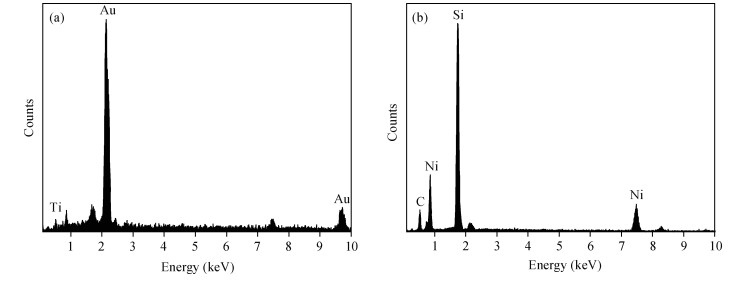
Table 1. The results of the wire-bonding tests performed by Royce instruments.

|
| [1] |
Lu W J, Mitchel W C, Landis G R, et al. Catalytic graphitization and ohmic contact formation on 4H-SiC. J Appl Phys, 2003, 93: 5397 doi: 10.1063/1.1562737
|
| [2] |
Han Ru, Yang Yintang, Wang Ping, et al. Ohmic contact properties of multi-metal film on n-type 4H-SiC. Chinese Journal of Semiconductors, 200728(2): 150 http://en.cnki.com.cn/Article_en/CJFDTOTAL-BDTX200702001.htm
|
| [3] |
Siad M, Abdesslam M, Chami A C. Role of carbon in the formation of ohmic contact in Ni/4H-SiC and Ni/Ti/4H-SiC. Appl Surf Sci, 2012, 258(18): 6819 doi: 10.1016/j.apsusc.2012.03.108
|
| [4] |
Nikitina I P, Vassilevski K V, Wright N G, et al. Formation and role of graphite and nickel silicide in nickel based ohmic contacts to n-type silicon carbide. J Appl Phys, 2005, 97: 5397 http://ieeexplore.ieee.org/xpls/abs_all.jsp?arnumber=5043728
|
| [5] |
Barda B, Machá P, Cicho S, et al. Thermal degradation of Ni-based Schottky contacts on 6H-SiC. Appl Surf Sci, 2011, 257(9): 4418 doi: 10.1016/j.apsusc.2010.12.077
|
| [6] |
Hallin C, Yakimova R, Pécz B, et al. Improved Ni ohmic contact on n-type 4H-SiC. J Electron Mater, 1997, 26: 119 doi: 10.1007/s11664-997-0136-2
|
| [7] |
Marinova T, Kakanakova-Georgieva A, Krastev V, et al. Nickel based ohmic contacts on SiC. Mater Sci Eng B-Solid State Materials for Advanced Technology, 1997, 46: 223 doi: 10.1016/S0921-5107(96)01981-2
|
| [8] |
Zhang Z, Teng J, Yuan W X, et al. Kinetic study of interfacial solid state reactions in the Ni/4H-SiC contact. Appl Surf Sci, 2009, 255: 6939 doi: 10.1016/j.apsusc.2009.03.018
|
| [9] |
Ohyanagi T, Onose Y, Watanabe A. Ti/Ni bilayer ohmic contact on 4H-SiC. J Vac Sci Technol B, 2008, 26: 1359 doi: 10.1116/1.2949116
|
| [10] |
Luckowski E D, Delucca J M, Williams J R, et al. Improved ohmic contact to n-type 4H and 6H-SiC using nichrome. J Electron Mater, 1998, 27: 330 doi: 10.1007/s11664-998-0410-y
|
| [11] |
Guo H, Zhang Y M, Qiao D Y, et al. The fabrication of nickel silicide ohmic contacts to n-type 6H-silicon carbide. Chin Phys, 2007, 16(6): 1753 doi: 10.1088/1009-1963/16/6/046
|
| [12] |
Cho N I, Jung K H, Choi Y. Improved ohmic contact to the n-type 4H-SiC semiconductor using cobalt silicides. Semicond Sci Technol, 2004, 19(3): 306 doi: 10.1088/0268-1242/19/3/003
|
| [13] |
Machá P, Barda B, Kudrnová M. Role of titanium in Ti/Ni ohmic contact on n-type 6H-SiC. Microelectron Eng, 2010, 87: 274 doi: 10.1016/j.mee.2009.06.017
|
| [14] |
Jae Hyun P, Holloway P H. Effects of nickel and titanium thickness on nickel/titanium ohmic contacts to n-type silicon carbide. J Vac Sci Technol B, 2005, 23: 486 doi: 10.1116/1.1868694
|
| [15] |
Wang Shouguo, Zhang Yan, Zhang Yimen, et al. Ohmic contacts of 4H-SiC on ion-implantation layers. Chin Phys B, 2010, 19: 017204 doi: 10.1088/1674-1056/19/1/017204
|
| [16] |
Cicho S, Machá P, Barda B, et al. Raman study of Ni and Ni silicide contacts on 4H-and 6H-SiC. Thin Solid Films, 2012, 520: 4378 doi: 10.1016/j.tsf.2012.02.008
|
| [17] |
Mercier F. Chaix-Pluchery O, Ouisse T, et al Raman scattering from Ti3SiC2 single crystals. Appl Phys Lett, 2011, 98: 081912 doi: 10.1063/1.3558919
|
| [18] |
Vishnyakov V, Lu J, Eklund P, et al. Ti3SiC2-formation during TieCeSi multilayer deposition by magnetron sputtering at 650℃. Rapid Commun, 2013, 93: 56 http://www.sciencedirect.com/science/article/pii/S0042207X13000067
|
| [19] |
Siad M, Abdesselam M, Souami N, et al. Structural characterization of Ni and Ni/Ti ohmic contact on n-type 4H-SiC. Appl Surf Sci, 2011, 257: 10737 doi: 10.1016/j.apsusc.2011.07.089
|
| [20] |
Pécz B. Contact formation in SiC devices. Appl Surf Sci, 2001, 184: 287 doi: 10.1016/S0169-4332(01)00678-X
|
| [21] |
Han S Y, Kim K H, Kim J K, et al. Ohmic contact formation mechanism of Ni on n-type 4H-SiC. Appl Phys Lett, 2001, 79: 3 http://ieeexplore.ieee.org/xpls/abs_all.jsp?arnumber=4894078
|
| [22] |
Kuchuk A, Kladko V, Guziewicz M, et al. Fabrication and characterization of nickel silicide ohmic contacts to n-type 4H silicon carbide. Journal of Physics Conference Series, 2008, 100: 042003 doi: 10.1088/1742-6596/100/4/042003
|


Article views: 4203 Times PDF downloads: 96 Times Cited by: 0 Times
Received: 19 December 2013 Revised: 28 February 2014 Online: Published: 01 July 2014
| Citation: |
Linchao Han, Huajun Shen, Kean Liu, Yiyu Wang, Yidan Tang, Yun Bai, Hengyu Xu, Yudong Wu, Xinyu Liu. Improved adhesion and interface ohmic contact on n-type 4H-SiC substrate by using Ni/Ti/Ni[J]. Journal of Semiconductors, 2014, 35(7): 072003. doi: 10.1088/1674-4926/35/7/072003
****
L C Han, H J Shen, K A Liu, Y Y Wang, Y D Tang, Y Bai, H Y Xu, Y D Wu, X Y Liu. Improved adhesion and interface ohmic contact on n-type 4H-SiC substrate by using Ni/Ti/Ni[J]. J. Semicond., 2014, 35(7): 072003. doi: 10.1088/1674-4926/35/7/072003.

|
| [1] |
Lu W J, Mitchel W C, Landis G R, et al. Catalytic graphitization and ohmic contact formation on 4H-SiC. J Appl Phys, 2003, 93: 5397 doi: 10.1063/1.1562737
|
| [2] |
Han Ru, Yang Yintang, Wang Ping, et al. Ohmic contact properties of multi-metal film on n-type 4H-SiC. Chinese Journal of Semiconductors, 200728(2): 150 http://en.cnki.com.cn/Article_en/CJFDTOTAL-BDTX200702001.htm
|
| [3] |
Siad M, Abdesslam M, Chami A C. Role of carbon in the formation of ohmic contact in Ni/4H-SiC and Ni/Ti/4H-SiC. Appl Surf Sci, 2012, 258(18): 6819 doi: 10.1016/j.apsusc.2012.03.108
|
| [4] |
Nikitina I P, Vassilevski K V, Wright N G, et al. Formation and role of graphite and nickel silicide in nickel based ohmic contacts to n-type silicon carbide. J Appl Phys, 2005, 97: 5397 http://ieeexplore.ieee.org/xpls/abs_all.jsp?arnumber=5043728
|
| [5] |
Barda B, Machá P, Cicho S, et al. Thermal degradation of Ni-based Schottky contacts on 6H-SiC. Appl Surf Sci, 2011, 257(9): 4418 doi: 10.1016/j.apsusc.2010.12.077
|
| [6] |
Hallin C, Yakimova R, Pécz B, et al. Improved Ni ohmic contact on n-type 4H-SiC. J Electron Mater, 1997, 26: 119 doi: 10.1007/s11664-997-0136-2
|
| [7] |
Marinova T, Kakanakova-Georgieva A, Krastev V, et al. Nickel based ohmic contacts on SiC. Mater Sci Eng B-Solid State Materials for Advanced Technology, 1997, 46: 223 doi: 10.1016/S0921-5107(96)01981-2
|
| [8] |
Zhang Z, Teng J, Yuan W X, et al. Kinetic study of interfacial solid state reactions in the Ni/4H-SiC contact. Appl Surf Sci, 2009, 255: 6939 doi: 10.1016/j.apsusc.2009.03.018
|
| [9] |
Ohyanagi T, Onose Y, Watanabe A. Ti/Ni bilayer ohmic contact on 4H-SiC. J Vac Sci Technol B, 2008, 26: 1359 doi: 10.1116/1.2949116
|
| [10] |
Luckowski E D, Delucca J M, Williams J R, et al. Improved ohmic contact to n-type 4H and 6H-SiC using nichrome. J Electron Mater, 1998, 27: 330 doi: 10.1007/s11664-998-0410-y
|
| [11] |
Guo H, Zhang Y M, Qiao D Y, et al. The fabrication of nickel silicide ohmic contacts to n-type 6H-silicon carbide. Chin Phys, 2007, 16(6): 1753 doi: 10.1088/1009-1963/16/6/046
|
| [12] |
Cho N I, Jung K H, Choi Y. Improved ohmic contact to the n-type 4H-SiC semiconductor using cobalt silicides. Semicond Sci Technol, 2004, 19(3): 306 doi: 10.1088/0268-1242/19/3/003
|
| [13] |
Machá P, Barda B, Kudrnová M. Role of titanium in Ti/Ni ohmic contact on n-type 6H-SiC. Microelectron Eng, 2010, 87: 274 doi: 10.1016/j.mee.2009.06.017
|
| [14] |
Jae Hyun P, Holloway P H. Effects of nickel and titanium thickness on nickel/titanium ohmic contacts to n-type silicon carbide. J Vac Sci Technol B, 2005, 23: 486 doi: 10.1116/1.1868694
|
| [15] |
Wang Shouguo, Zhang Yan, Zhang Yimen, et al. Ohmic contacts of 4H-SiC on ion-implantation layers. Chin Phys B, 2010, 19: 017204 doi: 10.1088/1674-1056/19/1/017204
|
| [16] |
Cicho S, Machá P, Barda B, et al. Raman study of Ni and Ni silicide contacts on 4H-and 6H-SiC. Thin Solid Films, 2012, 520: 4378 doi: 10.1016/j.tsf.2012.02.008
|
| [17] |
Mercier F. Chaix-Pluchery O, Ouisse T, et al Raman scattering from Ti3SiC2 single crystals. Appl Phys Lett, 2011, 98: 081912 doi: 10.1063/1.3558919
|
| [18] |
Vishnyakov V, Lu J, Eklund P, et al. Ti3SiC2-formation during TieCeSi multilayer deposition by magnetron sputtering at 650℃. Rapid Commun, 2013, 93: 56 http://www.sciencedirect.com/science/article/pii/S0042207X13000067
|
| [19] |
Siad M, Abdesselam M, Souami N, et al. Structural characterization of Ni and Ni/Ti ohmic contact on n-type 4H-SiC. Appl Surf Sci, 2011, 257: 10737 doi: 10.1016/j.apsusc.2011.07.089
|
| [20] |
Pécz B. Contact formation in SiC devices. Appl Surf Sci, 2001, 184: 287 doi: 10.1016/S0169-4332(01)00678-X
|
| [21] |
Han S Y, Kim K H, Kim J K, et al. Ohmic contact formation mechanism of Ni on n-type 4H-SiC. Appl Phys Lett, 2001, 79: 3 http://ieeexplore.ieee.org/xpls/abs_all.jsp?arnumber=4894078
|
| [22] |
Kuchuk A, Kladko V, Guziewicz M, et al. Fabrication and characterization of nickel silicide ohmic contacts to n-type 4H silicon carbide. Journal of Physics Conference Series, 2008, 100: 042003 doi: 10.1088/1742-6596/100/4/042003
|

 WeChat ID
Journal of Semiconductors © 2017 All Rights Reserved 京ICP备05085259号-2

 DownLoad:

