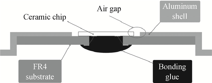
Fig. 1.
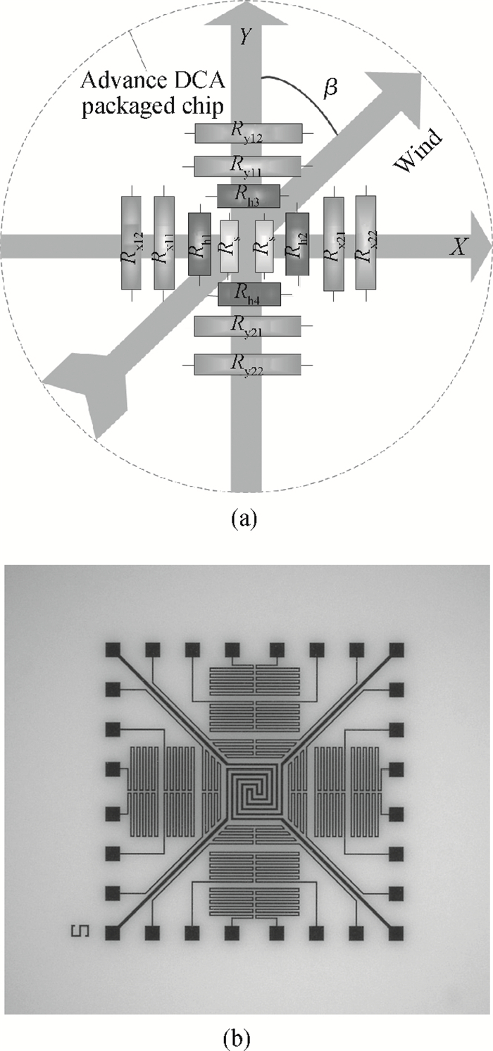
(a) Structure diagram of ceramic chip and (b) microscopic structure of ceramic chip.
SEMICONDUCTOR DEVICES
Lin Zhou, Ming Qin, Shengqi Chen and Bei Chen
Corresponding author: Qin Ming, Email:mqin@seu.edu.cn
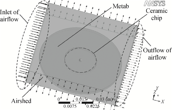
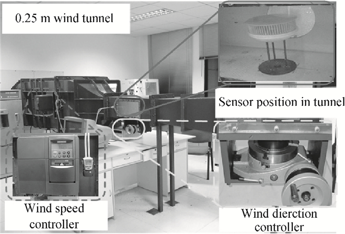
Abstract: An advanced direct chip attach packaged two-dimensional ceramic thermal wind sensor is studied. The thermal wind sensor chip is fabricated by metal lift-off processes on the ceramic substrate. An advanced direct chip attach (DCA) packaging is adopted and this new packaged method simplifies the processes of packaging further. Simulations of the advanced DCA packaged sensor based on computational fluid dynamics (CFD) model show the sensor can detect wind speed and direction effectively. The wind tunnel testing results show the advanced DCA packaged sensor can detect the wind direction from 0° to 360° and wind speed from 0 to 20 m/s with the error less than 0.5 m/s. The nonlinear fitting based least square method in Matlab is used to analyze the performance of the sensor.
Keywords: advanced direct chip attach package, CFD model, ceramic chip, thermal wind sensor
| [1] |
Huang Jinbao, Li Bin, Tong Qinyi, et al. A fully integrated flow sensor. Chinese Journal of Semiconductors, 1989, 10(1): 55(in Chinese) https://www.ama-science.org/proceedings/details/411
|
| [2] |
Van Oudheusden B W. Silicon thermal flow sensor with a two-dimensional direction sensitivity. Measurement Science and Technology, 1990, 1(7): 565 doi: 10.1088/0957-0233/1/7/005
|
| [3] |
Huang Jinbiao, Luo Zhiqiang, Feng Yaolan, et al. Flow velocity sensor fabricated by surface micromaching technology. Chinese Journal of Semiconductors, 1993, 14(7): 450(in Chinese)
|
| [4] |
Matova S P, Makinwa Kofi A A, Huijsing J H. Compensation of packaging asymmetry in a 2-D wind sensor. IEEE Sensor J, 2003, 3(6): 761 doi: 10.1109/JSEN.2003.820324
|
| [5] |
Gao Donghui, Qin Ming, Huang Qing'an. Thermal simulation of a silicon gas flow sensor and its packaging. Chinese Journal of Semiconductors, 2005, 26(2): 368(in Chinese)
|
| [6] |
Dong Ziqian, Chen Jingjing, Qin Yukun, et al. Fabrication of a micromachined two-dimensional wind sensor by Au-Au wafer bonding technology. J Microelectromechan Syst, 2012, 21(2): 465 http://ieeexplore.ieee.org/abstract/document/6125959
|
| [7] |
Shen Guangping, Wu Jian, Zhang Hua, et al. Direct chip attachment (DCA) packaging of a 2-D thermal flow sensor. 8th International Conference on Electronic Packaging Technology, Shanghai, 2007: 1 http://ieeexplore.ieee.org/document/4441487/authors
|
| [8] |
Shen Guangping, Wu Jian, Zhang Hua, et al. Design of a 2D thermal wind sensor based on MEMS process. Chinese Journal of Semiconductors, 2007, 28(11): 1830(in Chinese) http://en.cnki.com.cn/Article_en/CJFDTOTAL-BDTX200711032.htm
|
| [9] |
Makinwa K A A, Huijsing J H, Hagedoorn A. A solid-state 2-D wind sensor. 6th International Workshop of SAMOS, 2006: 477 http://www.springerlink.com/index/dw0107h363577855.pdf
|
| [10] |
Ansys ICEM CFD Help Manual, 2009: 136
|
| [11] |
Ansys Release 12. 0-CFX-Pre User's Guide, 2009: 101
|
| [12] |
Matlab 2012b Optimization Toolbox User's Guide, 2012: 375
|
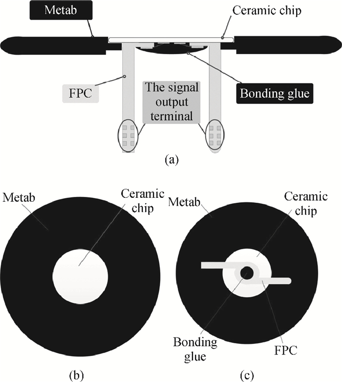
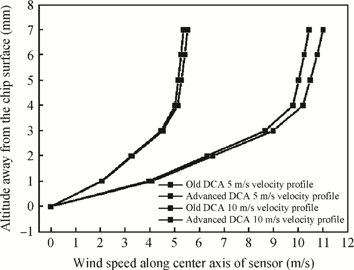
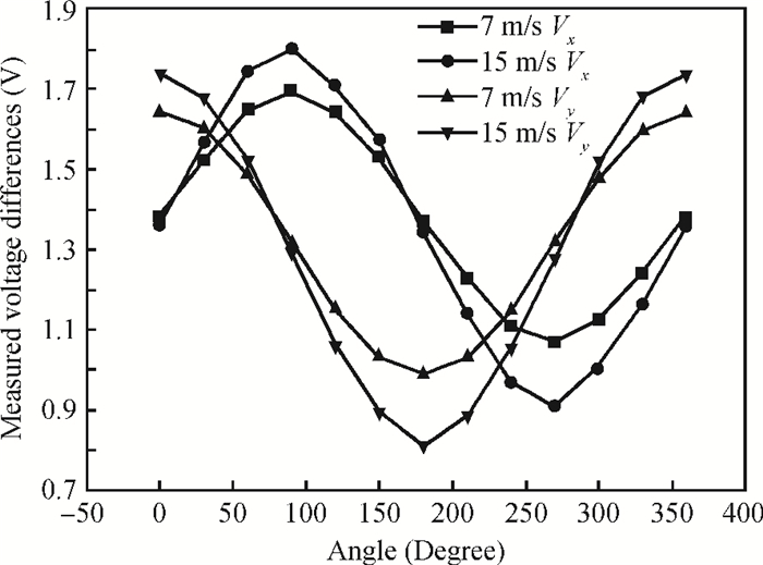


Table 1. The major parameters of the materials defined in the CFD model.

|
Table 2. Correspondence value of MCy and yield.

|
| [1] |
Huang Jinbao, Li Bin, Tong Qinyi, et al. A fully integrated flow sensor. Chinese Journal of Semiconductors, 1989, 10(1): 55(in Chinese) https://www.ama-science.org/proceedings/details/411
|
| [2] |
Van Oudheusden B W. Silicon thermal flow sensor with a two-dimensional direction sensitivity. Measurement Science and Technology, 1990, 1(7): 565 doi: 10.1088/0957-0233/1/7/005
|
| [3] |
Huang Jinbiao, Luo Zhiqiang, Feng Yaolan, et al. Flow velocity sensor fabricated by surface micromaching technology. Chinese Journal of Semiconductors, 1993, 14(7): 450(in Chinese)
|
| [4] |
Matova S P, Makinwa Kofi A A, Huijsing J H. Compensation of packaging asymmetry in a 2-D wind sensor. IEEE Sensor J, 2003, 3(6): 761 doi: 10.1109/JSEN.2003.820324
|
| [5] |
Gao Donghui, Qin Ming, Huang Qing'an. Thermal simulation of a silicon gas flow sensor and its packaging. Chinese Journal of Semiconductors, 2005, 26(2): 368(in Chinese)
|
| [6] |
Dong Ziqian, Chen Jingjing, Qin Yukun, et al. Fabrication of a micromachined two-dimensional wind sensor by Au-Au wafer bonding technology. J Microelectromechan Syst, 2012, 21(2): 465 http://ieeexplore.ieee.org/abstract/document/6125959
|
| [7] |
Shen Guangping, Wu Jian, Zhang Hua, et al. Direct chip attachment (DCA) packaging of a 2-D thermal flow sensor. 8th International Conference on Electronic Packaging Technology, Shanghai, 2007: 1 http://ieeexplore.ieee.org/document/4441487/authors
|
| [8] |
Shen Guangping, Wu Jian, Zhang Hua, et al. Design of a 2D thermal wind sensor based on MEMS process. Chinese Journal of Semiconductors, 2007, 28(11): 1830(in Chinese) http://en.cnki.com.cn/Article_en/CJFDTOTAL-BDTX200711032.htm
|
| [9] |
Makinwa K A A, Huijsing J H, Hagedoorn A. A solid-state 2-D wind sensor. 6th International Workshop of SAMOS, 2006: 477 http://www.springerlink.com/index/dw0107h363577855.pdf
|
| [10] |
Ansys ICEM CFD Help Manual, 2009: 136
|
| [11] |
Ansys Release 12. 0-CFX-Pre User's Guide, 2009: 101
|
| [12] |
Matlab 2012b Optimization Toolbox User's Guide, 2012: 375
|


Article views: 3264 Times PDF downloads: 23 Times Cited by: 0 Times
Received: 03 December 2013 Revised: 28 February 2014 Online: Published: 01 July 2014
| Citation: |
Lin Zhou, Ming Qin, Shengqi Chen, Bei Chen. Ceramic thermal wind sensor based on advanced direct chip attach package[J]. Journal of Semiconductors, 2014, 35(7): 074015. doi: 10.1088/1674-4926/35/7/074015
****
L Zhou, M Qin, S Q Chen, B Chen. Ceramic thermal wind sensor based on advanced direct chip attach package[J]. J. Semicond., 2014, 35(7): 074015. doi: 10.1088/1674-4926/35/7/074015.

|
| [1] |
Huang Jinbao, Li Bin, Tong Qinyi, et al. A fully integrated flow sensor. Chinese Journal of Semiconductors, 1989, 10(1): 55(in Chinese) https://www.ama-science.org/proceedings/details/411
|
| [2] |
Van Oudheusden B W. Silicon thermal flow sensor with a two-dimensional direction sensitivity. Measurement Science and Technology, 1990, 1(7): 565 doi: 10.1088/0957-0233/1/7/005
|
| [3] |
Huang Jinbiao, Luo Zhiqiang, Feng Yaolan, et al. Flow velocity sensor fabricated by surface micromaching technology. Chinese Journal of Semiconductors, 1993, 14(7): 450(in Chinese)
|
| [4] |
Matova S P, Makinwa Kofi A A, Huijsing J H. Compensation of packaging asymmetry in a 2-D wind sensor. IEEE Sensor J, 2003, 3(6): 761 doi: 10.1109/JSEN.2003.820324
|
| [5] |
Gao Donghui, Qin Ming, Huang Qing'an. Thermal simulation of a silicon gas flow sensor and its packaging. Chinese Journal of Semiconductors, 2005, 26(2): 368(in Chinese)
|
| [6] |
Dong Ziqian, Chen Jingjing, Qin Yukun, et al. Fabrication of a micromachined two-dimensional wind sensor by Au-Au wafer bonding technology. J Microelectromechan Syst, 2012, 21(2): 465 http://ieeexplore.ieee.org/abstract/document/6125959
|
| [7] |
Shen Guangping, Wu Jian, Zhang Hua, et al. Direct chip attachment (DCA) packaging of a 2-D thermal flow sensor. 8th International Conference on Electronic Packaging Technology, Shanghai, 2007: 1 http://ieeexplore.ieee.org/document/4441487/authors
|
| [8] |
Shen Guangping, Wu Jian, Zhang Hua, et al. Design of a 2D thermal wind sensor based on MEMS process. Chinese Journal of Semiconductors, 2007, 28(11): 1830(in Chinese) http://en.cnki.com.cn/Article_en/CJFDTOTAL-BDTX200711032.htm
|
| [9] |
Makinwa K A A, Huijsing J H, Hagedoorn A. A solid-state 2-D wind sensor. 6th International Workshop of SAMOS, 2006: 477 http://www.springerlink.com/index/dw0107h363577855.pdf
|
| [10] |
Ansys ICEM CFD Help Manual, 2009: 136
|
| [11] |
Ansys Release 12. 0-CFX-Pre User's Guide, 2009: 101
|
| [12] |
Matlab 2012b Optimization Toolbox User's Guide, 2012: 375
|

 WeChat ID
Journal of Semiconductors © 2017 All Rights Reserved 京ICP备05085259号-2

 DownLoad: