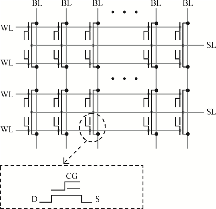
Fig. 1.
Common-source flash array using split-gate flash memory cell.
SEMICONDUCTOR INTEGRATED CIRCUITS
Shengbo Zhang1, 2, 3, , Guangjun Yang3, Jian Hu3 and Jun Xiao3
Corresponding author: Zhang Shengbo, Email:Baron.Zhang@hhgrace.com
Abstract: A novel sourceline voltage compensation circuit for program operation in embedded flash memory is presented. With the sourceline voltage compensation circuit, the charge pump can modulate the output voltage according to the number of cells to be programmed with data "0". So the IR drop on the sourceline decoding path is compensated, and a stable sourceline voltage can be obtained. In order to reduce the power dissipation in program operation, a bit-inversion program circuit is adopted. By using the bit-inversion program circuit, the cells programmed to data "0" are limited to half of the bits of a write data word, thus power dissipation in program operation is greatly reduced. A 1.8-V 8×64-kbits embedded NOR flash memory employing the two circuits has been integrated using a GSMC 0.18-μm 4-poly 4-metal CMOS process.
Keywords: charge pump, flash memory, sourceline voltage compensation circuit, split-gate flash memory cell
| [1] |
Strenz R. Embedded flash technologies and their applications: status and outlook. IEEE International Electron Devices Meeting (IEDM), 2011: 941
|
| [2] |
Sung H C, Lei T F, Hsu T H, et al. Novel program versus disturb window characterization for split-gate flash cell. IEEE Electron Device Lett, 2005, 26: 194 doi: 10.1109/LED.2004.842643
|
| [3] |
Kianian S, Levi A, Lee D, et al. A novel 3 volts-only, small sector erase, high density flash EPROM. Symposium on VLSI Technology, Digest of Technical Papers, 1994: 71
|
| [4] |
Yeh B. Single transistor non-volatile electrically alterable semiconductor memory device. USA Patent, No.5029130, 1991
|
| [5] |
Baek J M, Chun J H, Kwon K W. A power-efficient voltage upconverter for embedded EEPROM application. IEEE Trans Circuits Syst Ⅱ, Exp Briefs, 2010, 57(6): 435 doi: 10.1109/TCSII.2010.2048351
|
| [6] |
Kushnarenko A. Method and apparatus for reducing the number of programmed bits in a memory array. US Patent, No. 2003/0046481 A1, 2003 http://www.freepatentsonline.com/y2003/0046481.html
|
| [7] |
Seo M K, Sim S H, Oh M H, et al. A 130-nm 0.9-V 66-MHz 8- Mb (256KX32) local SONOS embedded flash EEPROM. IEEE J Solid-State Circuits, 2005, 40: 877 doi: 10.1109/JSSC.2005.845564
|
| [8] |
Seo M K, Lee H S. Circuit and method for controlling boosting voltage. US Patent, No.7120058 B2, 2005 http://www.freepatentsonline.com/y2005/0254304.html
|
| [9] |
Lin E, Ly A, Nguyen H Q, et al. Circuit for compensating programming current required, depending upon programming state. US Patent, No. 6853584 B2, 2005 http://www.freepatentsonline.com/y2004/0218422.html
|
| [10] |
Se-eun O. Boost voltage generating circuit and method thereof. US Patent, No.7499333 B2, 2009 http://www.freepatentsonline.com/7499333.html
|
| [11] |
Krzentz S V. Combined resistance–capacitance ladder voltage divider circuit. US Patent, No. 5796296, 1998 http://www.freepatentsonline.com/5796296.html
|
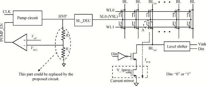
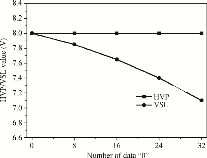
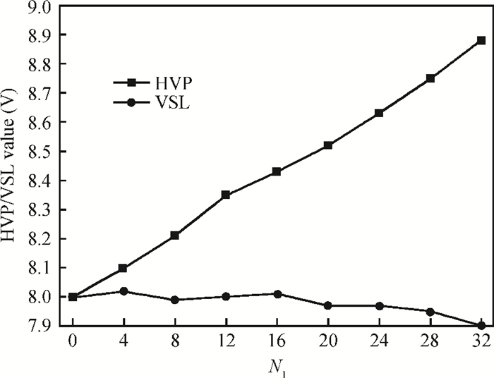
Table 1. Operation conditions of the split-gate flash cell.

|
| [1] |
Strenz R. Embedded flash technologies and their applications: status and outlook. IEEE International Electron Devices Meeting (IEDM), 2011: 941
|
| [2] |
Sung H C, Lei T F, Hsu T H, et al. Novel program versus disturb window characterization for split-gate flash cell. IEEE Electron Device Lett, 2005, 26: 194 doi: 10.1109/LED.2004.842643
|
| [3] |
Kianian S, Levi A, Lee D, et al. A novel 3 volts-only, small sector erase, high density flash EPROM. Symposium on VLSI Technology, Digest of Technical Papers, 1994: 71
|
| [4] |
Yeh B. Single transistor non-volatile electrically alterable semiconductor memory device. USA Patent, No.5029130, 1991
|
| [5] |
Baek J M, Chun J H, Kwon K W. A power-efficient voltage upconverter for embedded EEPROM application. IEEE Trans Circuits Syst Ⅱ, Exp Briefs, 2010, 57(6): 435 doi: 10.1109/TCSII.2010.2048351
|
| [6] |
Kushnarenko A. Method and apparatus for reducing the number of programmed bits in a memory array. US Patent, No. 2003/0046481 A1, 2003 http://www.freepatentsonline.com/y2003/0046481.html
|
| [7] |
Seo M K, Sim S H, Oh M H, et al. A 130-nm 0.9-V 66-MHz 8- Mb (256KX32) local SONOS embedded flash EEPROM. IEEE J Solid-State Circuits, 2005, 40: 877 doi: 10.1109/JSSC.2005.845564
|
| [8] |
Seo M K, Lee H S. Circuit and method for controlling boosting voltage. US Patent, No.7120058 B2, 2005 http://www.freepatentsonline.com/y2005/0254304.html
|
| [9] |
Lin E, Ly A, Nguyen H Q, et al. Circuit for compensating programming current required, depending upon programming state. US Patent, No. 6853584 B2, 2005 http://www.freepatentsonline.com/y2004/0218422.html
|
| [10] |
Se-eun O. Boost voltage generating circuit and method thereof. US Patent, No.7499333 B2, 2009 http://www.freepatentsonline.com/7499333.html
|
| [11] |
Krzentz S V. Combined resistance–capacitance ladder voltage divider circuit. US Patent, No. 5796296, 1998 http://www.freepatentsonline.com/5796296.html
|


Article views: 2524 Times PDF downloads: 20 Times Cited by: 0 Times
Received: 23 November 2013 Revised: 14 February 2014 Online: Published: 01 July 2014
| Citation: |
Shengbo Zhang, Guangjun Yang, Jian Hu, Jun Xiao. A novel sourceline voltage compensation circuit for embedded NOR flash memory[J]. Journal of Semiconductors, 2014, 35(7): 075007. doi: 10.1088/1674-4926/35/7/075007
****
S B Zhang, G J Yang, J Hu, J Xiao. A novel sourceline voltage compensation circuit for embedded NOR flash memory[J]. J. Semicond., 2014, 35(7): 075007. doi: 10.1088/1674-4926/35/7/075007.

|
| [1] |
Strenz R. Embedded flash technologies and their applications: status and outlook. IEEE International Electron Devices Meeting (IEDM), 2011: 941
|
| [2] |
Sung H C, Lei T F, Hsu T H, et al. Novel program versus disturb window characterization for split-gate flash cell. IEEE Electron Device Lett, 2005, 26: 194 doi: 10.1109/LED.2004.842643
|
| [3] |
Kianian S, Levi A, Lee D, et al. A novel 3 volts-only, small sector erase, high density flash EPROM. Symposium on VLSI Technology, Digest of Technical Papers, 1994: 71
|
| [4] |
Yeh B. Single transistor non-volatile electrically alterable semiconductor memory device. USA Patent, No.5029130, 1991
|
| [5] |
Baek J M, Chun J H, Kwon K W. A power-efficient voltage upconverter for embedded EEPROM application. IEEE Trans Circuits Syst Ⅱ, Exp Briefs, 2010, 57(6): 435 doi: 10.1109/TCSII.2010.2048351
|
| [6] |
Kushnarenko A. Method and apparatus for reducing the number of programmed bits in a memory array. US Patent, No. 2003/0046481 A1, 2003 http://www.freepatentsonline.com/y2003/0046481.html
|
| [7] |
Seo M K, Sim S H, Oh M H, et al. A 130-nm 0.9-V 66-MHz 8- Mb (256KX32) local SONOS embedded flash EEPROM. IEEE J Solid-State Circuits, 2005, 40: 877 doi: 10.1109/JSSC.2005.845564
|
| [8] |
Seo M K, Lee H S. Circuit and method for controlling boosting voltage. US Patent, No.7120058 B2, 2005 http://www.freepatentsonline.com/y2005/0254304.html
|
| [9] |
Lin E, Ly A, Nguyen H Q, et al. Circuit for compensating programming current required, depending upon programming state. US Patent, No. 6853584 B2, 2005 http://www.freepatentsonline.com/y2004/0218422.html
|
| [10] |
Se-eun O. Boost voltage generating circuit and method thereof. US Patent, No.7499333 B2, 2009 http://www.freepatentsonline.com/7499333.html
|
| [11] |
Krzentz S V. Combined resistance–capacitance ladder voltage divider circuit. US Patent, No. 5796296, 1998 http://www.freepatentsonline.com/5796296.html
|

 WeChat ID
Journal of Semiconductors © 2017 All Rights Reserved 京ICP备05085259号-2

 DownLoad: