


Fig. 1.
XRD patterns of the samples (a) before and (b) after annealing at 180 ℃ in air.
SEMICONDUCTOR MATERIALS
Liqin Hu, Dian Zhang, Hailong Hu and Tailiang Guo
Corresponding author: Hu Hailong, Email:huhl@fzu.edu.cn; Guo Tailiang, Email:gtl@fzu.edu.cn
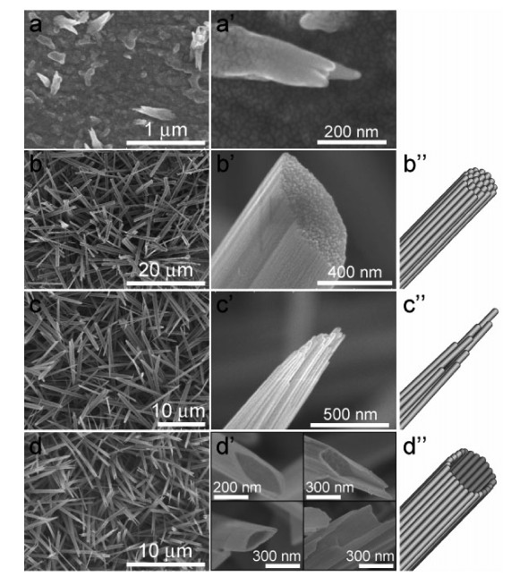
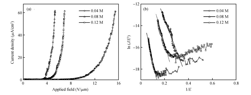
Abstract: One-dimensional CuO nanostructure arrays have been synthesized on Cu foil by a low-temperature wet chemical process. Different CuO nanostructures including nanorods with facet heads, nanorods with needle-like tips and nanotubes are shaped simply by varying the concentration of oxidant. Field emission measurements show that CuO nanorods with needle-like tips are of superior performance than other shapes, having a turn-on field of 3.5 V/μm and a field enhancement factor of 2107. The good field emission performance is assigned to the sharp tips contributing to the high field enhancement effect and to the moderate density reducing the field screening effect.
Keywords: 1D CuO nanostructure, oxidation, field emission
| [1] |
Saito Y, Uemura S. Field emission from carbon nanotubes and its application to electron sources. Carbon, 2000, 38: 169 doi: 10.1016/S0008-6223(99)00139-6
|
| [2] |
Dean K A, Chalamala B R. The environmental stability of field emission from single-walled carbon nanotubes. Appl Phys Lett, 1999, 75: 3017 doi: 10.1063/1.125219
|
| [3] |
Zhao Q, Zhang H Z, Zhu Y W, et al. Morphological effects on the field emission of ZnO nanorod arrays. Appl Phys Lett, 2005, 86: 203115 doi: 10.1063/1.1931831
|
| [4] |
Sung W, Kim W, Lee S, et al. Field emission characteristics of CuO nanowires by hydrogen plasma treatment. Vacuum, 2007, 81: 851 doi: 10.1016/j.vacuum.2006.10.002
|
| [5] |
He H, Wu T H, Hsin C L, et al. Beaklike SnO2 nanorods with strong photoluminescent and field-emission properties. Small, 2006, 2: 116 doi: 10.1002/(ISSN)1613-6829
|
| [6] |
Yue Shuanglin, Xu Tingting, Li Wei, et al. Tungsten oxide nanostructures: controllable growth and field emission. Journal of Semiconductors, 2012, 33(6): 063002 doi: 10.1088/1674-4926/33/6/063002
|
| [7] |
Zhu Y W, Yu T, Cheong F C, et al. Large-scale synthesis and field emission properties of vertically oriented CuO nanowire films. Nanotechnology, 2005, 16: 88 doi: 10.1088/0957-4484/16/1/018
|
| [8] |
Xu C, Liu Y, Xu G, et al. Preparation and characterization of CuO nanorods by thermal decomposition of CuC2O4 precursor. Mater Res Bull, 2002, 37: 2365 doi: 10.1016/S0025-5408(02)00848-6
|
| [9] |
Lu C, Qi L, Yang J, et al. Simple template-free solution route for the controlled synthesis of Cu(OH)2 and CuO nanostructures. J Phys Chem B, 2004, 108: 17825 doi: 10.1021/jp046772p
|
| [10] |
Jiang X, Herricks T, Xia Y. CuO nanowires can be synthesized by heating copper substrate in air. Nano Lett, 2002, 2: 1333 doi: 10.1021/nl0257519
|
| [11] |
Wang W, Varghese O K, Ruan C, et al. Synthesis of CuO and Cu2O crystalline nanowires using Cu(OH)2 nanowire templates. J Mater Res, 2003, 18: 2756 doi: 10.1557/JMR.2003.0384
|
| [12] |
Wen X, Zhang W, Yang S. Synthesis of Cu(OH)2 and CuO nanoribbon arrays on a copper surface. Langmuir, 2003, 19: 5898 doi: 10.1021/la0342870
|
| [13] |
Chen X, Kong L, Dong D, et al. Synthesis and characterization of superhydrophobic functionalized Cu(OH)2 nanotube arrays on copper foil. Appl Surf Sci, 2009, 255: 4015 doi: 10.1016/j.apsusc.2008.10.104
|
| [14] |
Wen X, Zhang W, Yang S. Solution phase synthesis of Cu(OH)2 nanoribbons by coordination self-assembly using Cu2S nanowires as precursors. Nano Lett, 2002, 2: 1397 doi: 10.1021/nl025848v
|
| [15] |
Gao P, Zhang M, Niu Z, et al. A facile solution-chemistry method for Cu(OH)2 nanoribbon arrays with noticeable electrochemical hydrogen storage ability at room temperature. Chem Commun, 2007, 43: 5197 http://europepmc.org/abstract/MED/18060140
|
| [16] |
Cao M, Hu C, Wang Y, et al. A controllable synthetic route to Cu, Cu2O, and CuO nanotubes and nanorods. Chem Comm, 2003: 1884 http://www.ncbi.nlm.nih.gov/pubmed/12932015
|
| [17] |
Chiguvare Z, Parisi J, Dyakonov V. Current limiting mechanisms in indium-tin-oxide/poly3-hexylthiophene/aluminum thin film devices. J Appl Phys, 2003, 94: 2440 doi: 10.1063/1.1588358
|
| [18] |
Wu J Q, Chen J, Deng S Z, et al. Field emission properties of α-Fe2O3 nanotips prepared on indium tin oxide coated glass by thermal oxidation of iron film. J Vac Sci Technol B, 2007, 28: C2B34 http://ieeexplore.ieee.org/xpls/abs_all.jsp?arnumber=5525364
|
| [19] |
Nilsson L, Groening O, Emmenegger C, et al. Scanning field emission from patterned carbon nanotube films. Appl Phys Lett, 2000, 76: 2071 doi: 10.1063/1.126258
|


Article views: 2763 Times PDF downloads: 24 Times Cited by: 0 Times
Received: 16 December 2013 Revised: 13 January 2014 Online: Published: 01 July 2014
| Citation: |
Liqin Hu, Dian Zhang, Hailong Hu, Tailiang Guo. Field electron emission from structure-controlled one-dimensional CuO arrays synthesized by wet chemical process[J]. Journal of Semiconductors, 2014, 35(7): 073003. doi: 10.1088/1674-4926/35/7/073003
****
L Q Hu, D Zhang, H L Hu, T L Guo. Field electron emission from structure-controlled one-dimensional CuO arrays synthesized by wet chemical process[J]. J. Semicond., 2014, 35(7): 073003. doi: 10.1088/1674-4926/35/7/073003.

|
| [1] |
Saito Y, Uemura S. Field emission from carbon nanotubes and its application to electron sources. Carbon, 2000, 38: 169 doi: 10.1016/S0008-6223(99)00139-6
|
| [2] |
Dean K A, Chalamala B R. The environmental stability of field emission from single-walled carbon nanotubes. Appl Phys Lett, 1999, 75: 3017 doi: 10.1063/1.125219
|
| [3] |
Zhao Q, Zhang H Z, Zhu Y W, et al. Morphological effects on the field emission of ZnO nanorod arrays. Appl Phys Lett, 2005, 86: 203115 doi: 10.1063/1.1931831
|
| [4] |
Sung W, Kim W, Lee S, et al. Field emission characteristics of CuO nanowires by hydrogen plasma treatment. Vacuum, 2007, 81: 851 doi: 10.1016/j.vacuum.2006.10.002
|
| [5] |
He H, Wu T H, Hsin C L, et al. Beaklike SnO2 nanorods with strong photoluminescent and field-emission properties. Small, 2006, 2: 116 doi: 10.1002/(ISSN)1613-6829
|
| [6] |
Yue Shuanglin, Xu Tingting, Li Wei, et al. Tungsten oxide nanostructures: controllable growth and field emission. Journal of Semiconductors, 2012, 33(6): 063002 doi: 10.1088/1674-4926/33/6/063002
|
| [7] |
Zhu Y W, Yu T, Cheong F C, et al. Large-scale synthesis and field emission properties of vertically oriented CuO nanowire films. Nanotechnology, 2005, 16: 88 doi: 10.1088/0957-4484/16/1/018
|
| [8] |
Xu C, Liu Y, Xu G, et al. Preparation and characterization of CuO nanorods by thermal decomposition of CuC2O4 precursor. Mater Res Bull, 2002, 37: 2365 doi: 10.1016/S0025-5408(02)00848-6
|
| [9] |
Lu C, Qi L, Yang J, et al. Simple template-free solution route for the controlled synthesis of Cu(OH)2 and CuO nanostructures. J Phys Chem B, 2004, 108: 17825 doi: 10.1021/jp046772p
|
| [10] |
Jiang X, Herricks T, Xia Y. CuO nanowires can be synthesized by heating copper substrate in air. Nano Lett, 2002, 2: 1333 doi: 10.1021/nl0257519
|
| [11] |
Wang W, Varghese O K, Ruan C, et al. Synthesis of CuO and Cu2O crystalline nanowires using Cu(OH)2 nanowire templates. J Mater Res, 2003, 18: 2756 doi: 10.1557/JMR.2003.0384
|
| [12] |
Wen X, Zhang W, Yang S. Synthesis of Cu(OH)2 and CuO nanoribbon arrays on a copper surface. Langmuir, 2003, 19: 5898 doi: 10.1021/la0342870
|
| [13] |
Chen X, Kong L, Dong D, et al. Synthesis and characterization of superhydrophobic functionalized Cu(OH)2 nanotube arrays on copper foil. Appl Surf Sci, 2009, 255: 4015 doi: 10.1016/j.apsusc.2008.10.104
|
| [14] |
Wen X, Zhang W, Yang S. Solution phase synthesis of Cu(OH)2 nanoribbons by coordination self-assembly using Cu2S nanowires as precursors. Nano Lett, 2002, 2: 1397 doi: 10.1021/nl025848v
|
| [15] |
Gao P, Zhang M, Niu Z, et al. A facile solution-chemistry method for Cu(OH)2 nanoribbon arrays with noticeable electrochemical hydrogen storage ability at room temperature. Chem Commun, 2007, 43: 5197 http://europepmc.org/abstract/MED/18060140
|
| [16] |
Cao M, Hu C, Wang Y, et al. A controllable synthetic route to Cu, Cu2O, and CuO nanotubes and nanorods. Chem Comm, 2003: 1884 http://www.ncbi.nlm.nih.gov/pubmed/12932015
|
| [17] |
Chiguvare Z, Parisi J, Dyakonov V. Current limiting mechanisms in indium-tin-oxide/poly3-hexylthiophene/aluminum thin film devices. J Appl Phys, 2003, 94: 2440 doi: 10.1063/1.1588358
|
| [18] |
Wu J Q, Chen J, Deng S Z, et al. Field emission properties of α-Fe2O3 nanotips prepared on indium tin oxide coated glass by thermal oxidation of iron film. J Vac Sci Technol B, 2007, 28: C2B34 http://ieeexplore.ieee.org/xpls/abs_all.jsp?arnumber=5525364
|
| [19] |
Nilsson L, Groening O, Emmenegger C, et al. Scanning field emission from patterned carbon nanotube films. Appl Phys Lett, 2000, 76: 2071 doi: 10.1063/1.126258
|

 WeChat ID
Journal of Semiconductors © 2017 All Rights Reserved 京ICP备05085259号-2

 DownLoad:

