


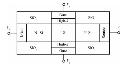
Fig. 1.
The simulated n-type double gate tunnel field effect transistor (DG-TFET)[1].
SEMICONDUCTOR DEVICES
M. W. Akram1, and Bahniman Ghosh1, 2,
Corresponding author: M. W. Akram, Email:mwakram@iitk.ac.in; Bahniman Ghosh, Email:bghosh@utexas.edu
Abstract: For the first time, we investigate the analog performance of n-type double gate junctionless tunnel field effect transistor (DG-JLTFET) and the results are compared with the conventional n-type double gate tunnel field effect transistor (DG-TFET) counterpart. Using extensive device simulations, the two devices are compared with the following analog performance parameters, namely transconductance, output conductance, output resistance, intrinsic gain, total gate capacitance and unity gain frequency. From the device simulation results, DG-JLTFET is found to have significantly better analog performance as compared to DG-TFET.
Keywords: junctionless field effect transistor, tunnel field effect transistor, subthreshold slope
| [1] |
Boucart K, Ionescu A M. Double-gate tunnel FET with high-k gate dielectric. IEEE Trans Electron Devices, 2007, 54: 1725 doi: 10.1109/TED.2007.899389
|
| [2] |
Koswatta S O, Lundstrom M S, Nikonov D E. Performance comparison between p-i-n tunneling transistors and conventional MOSFETs. IEEE Trans Electron Devices, 2009, 56(3): 456 doi: 10.1109/TED.2008.2011934
|
| [3] |
Nikam V, Bhuwalka K K, Kottantharayi A. Optimization of n-channel tunnel FET for the sub-22 nm gate length regime. Device Research Conference, Santa Barbara, CA, 2008 http://ieeexplore.ieee.org/xpls/abs_all.jsp?arnumber=4800742
|
| [4] |
Chaudhary A, Kumar M J. Controlling short-channel effects in deep-submicron SOI MOSFETs for improved reliability: a review. IEEE Trans Device Mater Reliab, 2004, 4: 99 doi: 10.1109/TDMR.2004.824359
|
| [5] |
Colinge J P. Multiple gate SOI MOSFETs. Solid-State Electron, 2004, 48: 897 doi: 10.1016/j.sse.2003.12.020
|
| [6] |
Chen Q, Bowman K A, Harrell E M, et al. Double jeopardy in the nanoscale court. IEEE Circuits Devices Mag, 2003, 19(1): 28 doi: 10.1109/MCD.2003.1175105
|
| [7] |
Reddick W, Amaratunga G A J. Silicon surface tunnel transistor. Appl Phys Lett, 1995, 67: 494 doi: 10.1063/1.114547
|
| [8] |
Appenzeller J, Lin Y M, Knoch J, et al. Band-to-band tunneling in carbon nanotube field-effect transistors. Phys Rev Lett, 2004, 93(19): 196805 doi: 10.1103/PhysRevLett.93.196805
|
| [9] |
Bhuwalka K, Sedlmaier S, Ludsteck A, et al. Vertical tunnel field-effect transistor. IEEE Trans Electron Devices, 2004, 51: 279 doi: 10.1109/TED.2003.821575
|
| [10] |
Zhang Q, Zhao W, Seabaugh A. Low-subthreshold-swing tunnel transistors. IEEE Electron Device Lett, 2006, 27(4): 297 doi: 10.1109/LED.2006.871855
|
| [11] |
Choi W Y, Park B G, Lee J D, et al. Tunneling field-effect transistors (TFETs) with subthreshold swing (SS) less than 60 mV/dec. IEEE Electron Device Lett, 2007, 28(8): 743 doi: 10.1109/LED.2007.901273
|
| [12] |
Boucart K, Ionescu A M. Length scaling of the double gate tunnel FET with a high-k gate dielectric. Solid-State Electron, 2007, 51: 1500 doi: 10.1016/j.sse.2007.09.014
|
| [13] |
Bjork M T, Knoch J, Schmid H, et al. Silicon nanowire tunneling field-effect transistors. Appl Phys Lett, 2008, 92: 193504 doi: 10.1063/1.2928227
|
| [14] |
Colinge J P, Lee C W, Afzalian A, et al. Nanowire transistors without junctions. Nat Nanotechnol, 2010, 5: 225 doi: 10.1038/nnano.2010.15
|
| [15] |
Lee C W, Afzalian A, Akhavan N D, et al. Junctionless multigate field-effect transistor. Appl Phys Lett, 2009, 94: 053511 doi: 10.1063/1.3079411
|
| [16] |
Lilienfeld J E. Method and apparatus for controlling electric current. US Patent, No. 1745175, Oct. 22, 1925
|
| [17] |
Colinge J P, Kranti A, Yan R, et al. Junctionless nanowire transistor (JNT): properties and design guidelines. Solid-State Electron, 2011, 65/66: 33 doi: 10.1016/j.sse.2011.06.004
|
| [18] |
Park C H, Ko M D, Kim K H, et al. Electrical characteristics of 20-nm junctionless Si nanowire transistors. Solid-State Electron, 2012, 73: 7 doi: 10.1016/j.sse.2011.11.032
|
| [19] |
Lee C W, Ferain I, Afzalian A, et al. Performance estimation of junctionless multigate transistors. Solid-State Electron, 2010, 54: 97 doi: 10.1016/j.sse.2009.12.003
|
| [20] |
Leung G, Chui C O. Variability impact of random dopant fluctuation on nanoscale junctionless FinFETs. IEEE Electron Device Lett, 2012, 33: 767 doi: 10.1109/LED.2012.2191931
|
| [21] |
Akhavan N D, Ferain I, Razavi P, et al. Random dopant variation in junctionless nanowire transistors. IEEE International SOI Conference (SOI), Tempe, Arizona, USA, 2011 http://ieeexplore.ieee.org/xpls/abs_all.jsp?arnumber=6081678
|
| [22] |
Ghosh B, Akram M W. Junctionless tunnel field effect transistor. IEEE Electron Device Lett, 2013, 34: 584 doi: 10.1109/LED.2013.2253752
|
| [23] |
Bal P, Akram M W, Mondal P, et al. Performance estimation of sub-30 nm junctionless tunnel FET (JLTFET). J Computational Electron, 2013, 12(4): 782 doi: 10.1007/s10825-013-0483-6
|
| [24] |
Lide D R. CRC handbook on chemistry and physics. 89th ed. London, UK: Taylor & Francis, 2008: 12
|
| [25] |
Silvaco, Version 5. 15. 32. R. (2009)[Online]. Available: http://www.silvaco.com
|
| [26] |
Schenk A. A model for the field and temperature dependence of SRH lifetimes in silicon. Solid-State Electron, 1992, 35: 1585 doi: 10.1016/0038-1101(92)90184-E
|
| [27] |
Flandre D, Raskin J P, Vanhoenacker D. SOI CMOS transistors for RF and microwave applications. Int J High Speed Electron Syst, 2001, 11: 1159 doi: 10.1142/S0129156401001076
|
| [28] |
Eggermont J P, Flandre D, Raskin J P, et al. Potential and modeling of 1m SOI CMOS operational transconductance amp lifiers for applications up to 1 GHz. IEEE J Solid-State Circuits, 1998, 33: 640 doi: 10.1109/4.663571
|
| [29] |
Silveira F, Flandre D, Jespers P G A. A gm/ID based methodology for the design of CMOS analog circuits and its application to the synthesis of a silicon-on-insulator micropower OTA. IEEE J Solid-State Circuits, 1996, 31: 1314 doi: 10.1109/4.535416
|
| [30] |
Flandre D, Ferreira L, Jespers P G A, et al. Modeling and application of fully-depleted SOI MOSFET's for low-voltage low-power analog CMOS circuits. Solid-State Electron, 1996, 39: 455 doi: 10.1016/0038-1101(95)00167-0
|
| [31] |
Kilchytska V, Néve A, Vancaillie L, et al. Influence of device engineering on the analog and RF performances of SOI MOSFETs. IEEE Trans Electron Devices, 2003, 50(3): 577 doi: 10.1109/TED.2003.810471
|
| [32] |
Gupta S K, Baishya S. Analog and RF performance evaluation of dual metal double gate high-k stack (DMDG-HKS) MOSFETs. J Nano Electron Phys, 2013, 5(3): 03008 http://connection.ebscohost.com/c/articles/91590443/analog-rf-performance-evaluation-dual-metal-double-gate-high-k-stack-dmdg-hks-mosfets
|
| [33] |
Narang R, Saxena M, GuptaR S, et al. Linearity and analog performance analysis of double gate tunnel FET: effect of temperature and gate stack. International Journal of VLSI Design & Communication Systems (VLSICS) 2011, 2(3): 185 doi: 10.1007/978-3-642-22543-7_47
|
| [34] |
Baruah R K, Paily R P. Analog performance of bulk planar junctionless transistor (BPJLT). Third International Conference on Computing, Communication and Networking Technologies (ICCCNT'12), Coimbatore, India, 2012 http://ieeexplore.ieee.org/document/6395875/
|
| [35] |
Mohankumar N, Syamal B, Sarkar C K. Investigation of novel attributes of single halo dual-material double gate MOSFETs for analog/RF applications. Microelectron Rel, 2009, 49: 1491 doi: 10.1016/j.microrel.2009.06.006
|
| [36] |
Esame O, Gurbuz Y, Tekin I, et al. Performance comparison of state-of-the-art heterojunction bipolar devices (HBT) based on AlGaAs/GaAs, Si/SiGe and InGaAs/InP. Microelectron J, 2004, 35: 901 doi: 10.1016/j.mejo.2004.07.003
|
| [37] |
Fobelets K, Calvo-Gallego J, Vel'azquez-P'erez J E. Effect of the gate scaling on the analogue performance of s-Si CMOS devices. Semicond Sci Technol, 2011, 26: 095030 doi: 10.1088/0268-1242/26/9/095030
|
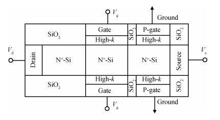
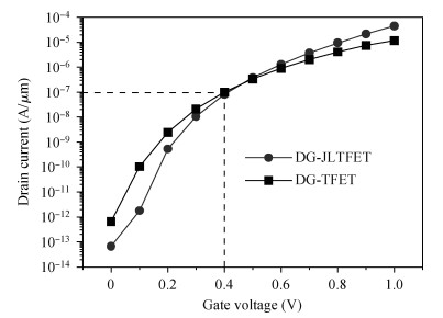
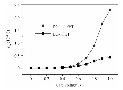
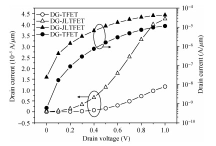
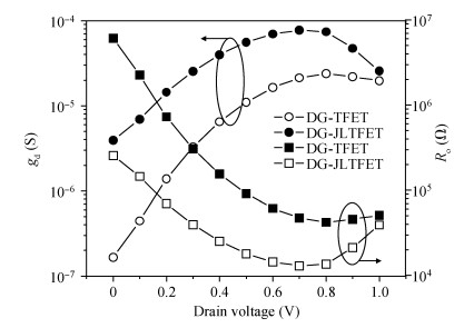
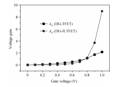
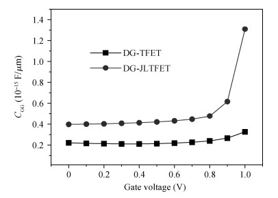
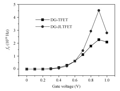
Table 1. Parameters used for the DG-TFET simulation.

|
Table 2. Parameters used for the DG-JLTFET simulation.

|
| [1] |
Boucart K, Ionescu A M. Double-gate tunnel FET with high-k gate dielectric. IEEE Trans Electron Devices, 2007, 54: 1725 doi: 10.1109/TED.2007.899389
|
| [2] |
Koswatta S O, Lundstrom M S, Nikonov D E. Performance comparison between p-i-n tunneling transistors and conventional MOSFETs. IEEE Trans Electron Devices, 2009, 56(3): 456 doi: 10.1109/TED.2008.2011934
|
| [3] |
Nikam V, Bhuwalka K K, Kottantharayi A. Optimization of n-channel tunnel FET for the sub-22 nm gate length regime. Device Research Conference, Santa Barbara, CA, 2008 http://ieeexplore.ieee.org/xpls/abs_all.jsp?arnumber=4800742
|
| [4] |
Chaudhary A, Kumar M J. Controlling short-channel effects in deep-submicron SOI MOSFETs for improved reliability: a review. IEEE Trans Device Mater Reliab, 2004, 4: 99 doi: 10.1109/TDMR.2004.824359
|
| [5] |
Colinge J P. Multiple gate SOI MOSFETs. Solid-State Electron, 2004, 48: 897 doi: 10.1016/j.sse.2003.12.020
|
| [6] |
Chen Q, Bowman K A, Harrell E M, et al. Double jeopardy in the nanoscale court. IEEE Circuits Devices Mag, 2003, 19(1): 28 doi: 10.1109/MCD.2003.1175105
|
| [7] |
Reddick W, Amaratunga G A J. Silicon surface tunnel transistor. Appl Phys Lett, 1995, 67: 494 doi: 10.1063/1.114547
|
| [8] |
Appenzeller J, Lin Y M, Knoch J, et al. Band-to-band tunneling in carbon nanotube field-effect transistors. Phys Rev Lett, 2004, 93(19): 196805 doi: 10.1103/PhysRevLett.93.196805
|
| [9] |
Bhuwalka K, Sedlmaier S, Ludsteck A, et al. Vertical tunnel field-effect transistor. IEEE Trans Electron Devices, 2004, 51: 279 doi: 10.1109/TED.2003.821575
|
| [10] |
Zhang Q, Zhao W, Seabaugh A. Low-subthreshold-swing tunnel transistors. IEEE Electron Device Lett, 2006, 27(4): 297 doi: 10.1109/LED.2006.871855
|
| [11] |
Choi W Y, Park B G, Lee J D, et al. Tunneling field-effect transistors (TFETs) with subthreshold swing (SS) less than 60 mV/dec. IEEE Electron Device Lett, 2007, 28(8): 743 doi: 10.1109/LED.2007.901273
|
| [12] |
Boucart K, Ionescu A M. Length scaling of the double gate tunnel FET with a high-k gate dielectric. Solid-State Electron, 2007, 51: 1500 doi: 10.1016/j.sse.2007.09.014
|
| [13] |
Bjork M T, Knoch J, Schmid H, et al. Silicon nanowire tunneling field-effect transistors. Appl Phys Lett, 2008, 92: 193504 doi: 10.1063/1.2928227
|
| [14] |
Colinge J P, Lee C W, Afzalian A, et al. Nanowire transistors without junctions. Nat Nanotechnol, 2010, 5: 225 doi: 10.1038/nnano.2010.15
|
| [15] |
Lee C W, Afzalian A, Akhavan N D, et al. Junctionless multigate field-effect transistor. Appl Phys Lett, 2009, 94: 053511 doi: 10.1063/1.3079411
|
| [16] |
Lilienfeld J E. Method and apparatus for controlling electric current. US Patent, No. 1745175, Oct. 22, 1925
|
| [17] |
Colinge J P, Kranti A, Yan R, et al. Junctionless nanowire transistor (JNT): properties and design guidelines. Solid-State Electron, 2011, 65/66: 33 doi: 10.1016/j.sse.2011.06.004
|
| [18] |
Park C H, Ko M D, Kim K H, et al. Electrical characteristics of 20-nm junctionless Si nanowire transistors. Solid-State Electron, 2012, 73: 7 doi: 10.1016/j.sse.2011.11.032
|
| [19] |
Lee C W, Ferain I, Afzalian A, et al. Performance estimation of junctionless multigate transistors. Solid-State Electron, 2010, 54: 97 doi: 10.1016/j.sse.2009.12.003
|
| [20] |
Leung G, Chui C O. Variability impact of random dopant fluctuation on nanoscale junctionless FinFETs. IEEE Electron Device Lett, 2012, 33: 767 doi: 10.1109/LED.2012.2191931
|
| [21] |
Akhavan N D, Ferain I, Razavi P, et al. Random dopant variation in junctionless nanowire transistors. IEEE International SOI Conference (SOI), Tempe, Arizona, USA, 2011 http://ieeexplore.ieee.org/xpls/abs_all.jsp?arnumber=6081678
|
| [22] |
Ghosh B, Akram M W. Junctionless tunnel field effect transistor. IEEE Electron Device Lett, 2013, 34: 584 doi: 10.1109/LED.2013.2253752
|
| [23] |
Bal P, Akram M W, Mondal P, et al. Performance estimation of sub-30 nm junctionless tunnel FET (JLTFET). J Computational Electron, 2013, 12(4): 782 doi: 10.1007/s10825-013-0483-6
|
| [24] |
Lide D R. CRC handbook on chemistry and physics. 89th ed. London, UK: Taylor & Francis, 2008: 12
|
| [25] |
Silvaco, Version 5. 15. 32. R. (2009)[Online]. Available: http://www.silvaco.com
|
| [26] |
Schenk A. A model for the field and temperature dependence of SRH lifetimes in silicon. Solid-State Electron, 1992, 35: 1585 doi: 10.1016/0038-1101(92)90184-E
|
| [27] |
Flandre D, Raskin J P, Vanhoenacker D. SOI CMOS transistors for RF and microwave applications. Int J High Speed Electron Syst, 2001, 11: 1159 doi: 10.1142/S0129156401001076
|
| [28] |
Eggermont J P, Flandre D, Raskin J P, et al. Potential and modeling of 1m SOI CMOS operational transconductance amp lifiers for applications up to 1 GHz. IEEE J Solid-State Circuits, 1998, 33: 640 doi: 10.1109/4.663571
|
| [29] |
Silveira F, Flandre D, Jespers P G A. A gm/ID based methodology for the design of CMOS analog circuits and its application to the synthesis of a silicon-on-insulator micropower OTA. IEEE J Solid-State Circuits, 1996, 31: 1314 doi: 10.1109/4.535416
|
| [30] |
Flandre D, Ferreira L, Jespers P G A, et al. Modeling and application of fully-depleted SOI MOSFET's for low-voltage low-power analog CMOS circuits. Solid-State Electron, 1996, 39: 455 doi: 10.1016/0038-1101(95)00167-0
|
| [31] |
Kilchytska V, Néve A, Vancaillie L, et al. Influence of device engineering on the analog and RF performances of SOI MOSFETs. IEEE Trans Electron Devices, 2003, 50(3): 577 doi: 10.1109/TED.2003.810471
|
| [32] |
Gupta S K, Baishya S. Analog and RF performance evaluation of dual metal double gate high-k stack (DMDG-HKS) MOSFETs. J Nano Electron Phys, 2013, 5(3): 03008 http://connection.ebscohost.com/c/articles/91590443/analog-rf-performance-evaluation-dual-metal-double-gate-high-k-stack-dmdg-hks-mosfets
|
| [33] |
Narang R, Saxena M, GuptaR S, et al. Linearity and analog performance analysis of double gate tunnel FET: effect of temperature and gate stack. International Journal of VLSI Design & Communication Systems (VLSICS) 2011, 2(3): 185 doi: 10.1007/978-3-642-22543-7_47
|
| [34] |
Baruah R K, Paily R P. Analog performance of bulk planar junctionless transistor (BPJLT). Third International Conference on Computing, Communication and Networking Technologies (ICCCNT'12), Coimbatore, India, 2012 http://ieeexplore.ieee.org/document/6395875/
|
| [35] |
Mohankumar N, Syamal B, Sarkar C K. Investigation of novel attributes of single halo dual-material double gate MOSFETs for analog/RF applications. Microelectron Rel, 2009, 49: 1491 doi: 10.1016/j.microrel.2009.06.006
|
| [36] |
Esame O, Gurbuz Y, Tekin I, et al. Performance comparison of state-of-the-art heterojunction bipolar devices (HBT) based on AlGaAs/GaAs, Si/SiGe and InGaAs/InP. Microelectron J, 2004, 35: 901 doi: 10.1016/j.mejo.2004.07.003
|
| [37] |
Fobelets K, Calvo-Gallego J, Vel'azquez-P'erez J E. Effect of the gate scaling on the analogue performance of s-Si CMOS devices. Semicond Sci Technol, 2011, 26: 095030 doi: 10.1088/0268-1242/26/9/095030
|


Article views: 3347 Times PDF downloads: 35 Times Cited by: 0 Times
Received: 04 January 2014 Revised: 29 January 2014 Online: Published: 01 July 2014
| Citation: |
M. W. Akram, Bahniman Ghosh. Analog performance of double gate junctionless tunnel field effect transistor[J]. Journal of Semiconductors, 2014, 35(7): 074001. doi: 10.1088/1674-4926/35/7/074001
****
M. W. Akram, B Ghosh. Analog performance of double gate junctionless tunnel field effect transistor[J]. J. Semicond., 2014, 35(7): 074001. doi: 10.1088/1674-4926/35/7/074001.

|
| [1] |
Boucart K, Ionescu A M. Double-gate tunnel FET with high-k gate dielectric. IEEE Trans Electron Devices, 2007, 54: 1725 doi: 10.1109/TED.2007.899389
|
| [2] |
Koswatta S O, Lundstrom M S, Nikonov D E. Performance comparison between p-i-n tunneling transistors and conventional MOSFETs. IEEE Trans Electron Devices, 2009, 56(3): 456 doi: 10.1109/TED.2008.2011934
|
| [3] |
Nikam V, Bhuwalka K K, Kottantharayi A. Optimization of n-channel tunnel FET for the sub-22 nm gate length regime. Device Research Conference, Santa Barbara, CA, 2008 http://ieeexplore.ieee.org/xpls/abs_all.jsp?arnumber=4800742
|
| [4] |
Chaudhary A, Kumar M J. Controlling short-channel effects in deep-submicron SOI MOSFETs for improved reliability: a review. IEEE Trans Device Mater Reliab, 2004, 4: 99 doi: 10.1109/TDMR.2004.824359
|
| [5] |
Colinge J P. Multiple gate SOI MOSFETs. Solid-State Electron, 2004, 48: 897 doi: 10.1016/j.sse.2003.12.020
|
| [6] |
Chen Q, Bowman K A, Harrell E M, et al. Double jeopardy in the nanoscale court. IEEE Circuits Devices Mag, 2003, 19(1): 28 doi: 10.1109/MCD.2003.1175105
|
| [7] |
Reddick W, Amaratunga G A J. Silicon surface tunnel transistor. Appl Phys Lett, 1995, 67: 494 doi: 10.1063/1.114547
|
| [8] |
Appenzeller J, Lin Y M, Knoch J, et al. Band-to-band tunneling in carbon nanotube field-effect transistors. Phys Rev Lett, 2004, 93(19): 196805 doi: 10.1103/PhysRevLett.93.196805
|
| [9] |
Bhuwalka K, Sedlmaier S, Ludsteck A, et al. Vertical tunnel field-effect transistor. IEEE Trans Electron Devices, 2004, 51: 279 doi: 10.1109/TED.2003.821575
|
| [10] |
Zhang Q, Zhao W, Seabaugh A. Low-subthreshold-swing tunnel transistors. IEEE Electron Device Lett, 2006, 27(4): 297 doi: 10.1109/LED.2006.871855
|
| [11] |
Choi W Y, Park B G, Lee J D, et al. Tunneling field-effect transistors (TFETs) with subthreshold swing (SS) less than 60 mV/dec. IEEE Electron Device Lett, 2007, 28(8): 743 doi: 10.1109/LED.2007.901273
|
| [12] |
Boucart K, Ionescu A M. Length scaling of the double gate tunnel FET with a high-k gate dielectric. Solid-State Electron, 2007, 51: 1500 doi: 10.1016/j.sse.2007.09.014
|
| [13] |
Bjork M T, Knoch J, Schmid H, et al. Silicon nanowire tunneling field-effect transistors. Appl Phys Lett, 2008, 92: 193504 doi: 10.1063/1.2928227
|
| [14] |
Colinge J P, Lee C W, Afzalian A, et al. Nanowire transistors without junctions. Nat Nanotechnol, 2010, 5: 225 doi: 10.1038/nnano.2010.15
|
| [15] |
Lee C W, Afzalian A, Akhavan N D, et al. Junctionless multigate field-effect transistor. Appl Phys Lett, 2009, 94: 053511 doi: 10.1063/1.3079411
|
| [16] |
Lilienfeld J E. Method and apparatus for controlling electric current. US Patent, No. 1745175, Oct. 22, 1925
|
| [17] |
Colinge J P, Kranti A, Yan R, et al. Junctionless nanowire transistor (JNT): properties and design guidelines. Solid-State Electron, 2011, 65/66: 33 doi: 10.1016/j.sse.2011.06.004
|
| [18] |
Park C H, Ko M D, Kim K H, et al. Electrical characteristics of 20-nm junctionless Si nanowire transistors. Solid-State Electron, 2012, 73: 7 doi: 10.1016/j.sse.2011.11.032
|
| [19] |
Lee C W, Ferain I, Afzalian A, et al. Performance estimation of junctionless multigate transistors. Solid-State Electron, 2010, 54: 97 doi: 10.1016/j.sse.2009.12.003
|
| [20] |
Leung G, Chui C O. Variability impact of random dopant fluctuation on nanoscale junctionless FinFETs. IEEE Electron Device Lett, 2012, 33: 767 doi: 10.1109/LED.2012.2191931
|
| [21] |
Akhavan N D, Ferain I, Razavi P, et al. Random dopant variation in junctionless nanowire transistors. IEEE International SOI Conference (SOI), Tempe, Arizona, USA, 2011 http://ieeexplore.ieee.org/xpls/abs_all.jsp?arnumber=6081678
|
| [22] |
Ghosh B, Akram M W. Junctionless tunnel field effect transistor. IEEE Electron Device Lett, 2013, 34: 584 doi: 10.1109/LED.2013.2253752
|
| [23] |
Bal P, Akram M W, Mondal P, et al. Performance estimation of sub-30 nm junctionless tunnel FET (JLTFET). J Computational Electron, 2013, 12(4): 782 doi: 10.1007/s10825-013-0483-6
|
| [24] |
Lide D R. CRC handbook on chemistry and physics. 89th ed. London, UK: Taylor & Francis, 2008: 12
|
| [25] |
Silvaco, Version 5. 15. 32. R. (2009)[Online]. Available: http://www.silvaco.com
|
| [26] |
Schenk A. A model for the field and temperature dependence of SRH lifetimes in silicon. Solid-State Electron, 1992, 35: 1585 doi: 10.1016/0038-1101(92)90184-E
|
| [27] |
Flandre D, Raskin J P, Vanhoenacker D. SOI CMOS transistors for RF and microwave applications. Int J High Speed Electron Syst, 2001, 11: 1159 doi: 10.1142/S0129156401001076
|
| [28] |
Eggermont J P, Flandre D, Raskin J P, et al. Potential and modeling of 1m SOI CMOS operational transconductance amp lifiers for applications up to 1 GHz. IEEE J Solid-State Circuits, 1998, 33: 640 doi: 10.1109/4.663571
|
| [29] |
Silveira F, Flandre D, Jespers P G A. A gm/ID based methodology for the design of CMOS analog circuits and its application to the synthesis of a silicon-on-insulator micropower OTA. IEEE J Solid-State Circuits, 1996, 31: 1314 doi: 10.1109/4.535416
|
| [30] |
Flandre D, Ferreira L, Jespers P G A, et al. Modeling and application of fully-depleted SOI MOSFET's for low-voltage low-power analog CMOS circuits. Solid-State Electron, 1996, 39: 455 doi: 10.1016/0038-1101(95)00167-0
|
| [31] |
Kilchytska V, Néve A, Vancaillie L, et al. Influence of device engineering on the analog and RF performances of SOI MOSFETs. IEEE Trans Electron Devices, 2003, 50(3): 577 doi: 10.1109/TED.2003.810471
|
| [32] |
Gupta S K, Baishya S. Analog and RF performance evaluation of dual metal double gate high-k stack (DMDG-HKS) MOSFETs. J Nano Electron Phys, 2013, 5(3): 03008 http://connection.ebscohost.com/c/articles/91590443/analog-rf-performance-evaluation-dual-metal-double-gate-high-k-stack-dmdg-hks-mosfets
|
| [33] |
Narang R, Saxena M, GuptaR S, et al. Linearity and analog performance analysis of double gate tunnel FET: effect of temperature and gate stack. International Journal of VLSI Design & Communication Systems (VLSICS) 2011, 2(3): 185 doi: 10.1007/978-3-642-22543-7_47
|
| [34] |
Baruah R K, Paily R P. Analog performance of bulk planar junctionless transistor (BPJLT). Third International Conference on Computing, Communication and Networking Technologies (ICCCNT'12), Coimbatore, India, 2012 http://ieeexplore.ieee.org/document/6395875/
|
| [35] |
Mohankumar N, Syamal B, Sarkar C K. Investigation of novel attributes of single halo dual-material double gate MOSFETs for analog/RF applications. Microelectron Rel, 2009, 49: 1491 doi: 10.1016/j.microrel.2009.06.006
|
| [36] |
Esame O, Gurbuz Y, Tekin I, et al. Performance comparison of state-of-the-art heterojunction bipolar devices (HBT) based on AlGaAs/GaAs, Si/SiGe and InGaAs/InP. Microelectron J, 2004, 35: 901 doi: 10.1016/j.mejo.2004.07.003
|
| [37] |
Fobelets K, Calvo-Gallego J, Vel'azquez-P'erez J E. Effect of the gate scaling on the analogue performance of s-Si CMOS devices. Semicond Sci Technol, 2011, 26: 095030 doi: 10.1088/0268-1242/26/9/095030
|

 WeChat ID
Journal of Semiconductors © 2017 All Rights Reserved 京ICP备05085259号-2

 DownLoad:

