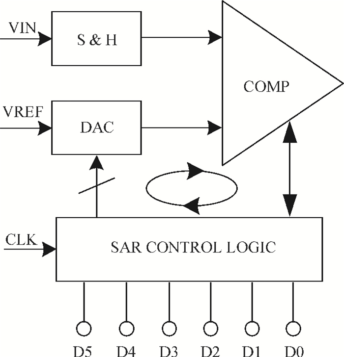
Fig. 1.
The block diagram of conventional SAR ADC.
SEMICONDUCTOR INTEGRATED CIRCUITS
Xue Han, Qi Wei, Huazhong Yang and Hui Wang
Corresponding author: Han Xue, Email:snowhx1988@163.com
Abstract: This paper proposes a single channel, 6-bit 230-MS/s asynchronous successive approximation register analog-to-digital converter (ADC) in an SMIC 65 nm CMOS technology. Through adopting the modified 2 bits/stage asynchronous control logic, the presented ADC actualizes a peak 40.90-dB spurious-free dynamic range and 29.05-dB signal-to-noise and distortion ratio at 230-MS/s sampling rate. Utilizing the dynamic comparator without the preamplifier, this work attains low-power design with only 0.93 mW power consumption and accomplishes a figure of merit of 174.67 fJ/step at 1 V supply voltage.
Keywords: analog-to-digital converter, successive approximation register, asynchronous control logic, 2bits per stage
| [1] |
Nuzzo P, Nani C, Armiento C, et al. A 6-bit 50-MS/s threshold configuring SAR ADC in 90-nm digital CMOS. IEEE Trans Circuits Syst I, 2012, 59(1): 80 doi: 10.1109/TCSI.2011.2161368
|
| [2] |
Van Elzakker M, van Tuijl E, Geraedts P, et al. A 1.9μW 4.4 fJ/conversion-step 10 b 1 MS/s charge-redistribution ADC. IEEE ISSCC Dig Tech Papers, 2008: 244
|
| [3] |
Chen S W M, Brodersen R W. A 6 b 600 MS/s 5.3 mW asynchronous ADC in 0.13μm CMOS. IEEE J Solid-State Circuits, 2006, 41(12): 2669 doi: 10.1109/JSSC.2006.884231
|
| [4] |
Lin Y Z, Hang S J, Liu Y T, et al. An asynchronous binary-search ADC architecture with a reduced comparator count. IEEE Trans Circuits Syst I, 2010, 57(8): 1829 doi: 10.1109/TCSI.2009.2037403
|
| [5] |
Jiang T, Liu W, Zhong F Y, et al. A single-channel, 1.25-GS/s, 6-bit, 6.08-mW asynchronous successive-approximation ADC with improved feedback delay in 40-nm CMOS. IEEE J Solid-State Circuits, 2012, 47(10): 2444 doi: 10.1109/JSSC.2012.2204543
|
| [6] |
Van der Plas G, Verbruggen B. A 150 MS/s 133μW 7 b ADC in 90 nm digital CMOS using a comparator-based asynchronous binary-search sub-ADC. IEEE International Solid-State Circuits Conference (ISSCC), 2008: 242
|
| [7] |
Han Xue, Fan Hua, Wei Qi, et al. A high SFDR 6-bit 20MS/s SAR ADC based on time-domain comparator. Journal of Semiconductors, 2013, 34(8): 085008 doi: 10.1088/1674-4926/34/8/085008
|
| [8] |
Wei H, Chan C H, Chio, U F et al. An 8-b 400-MS/s 2-b-per-cycle SAR ADC with resistive DAC. IEEE J Solid-State Circuits, 2012, 47(11): 2763 doi: 10.1109/JSSC.2012.2214181
|
| [9] |
Mesgarani A, Ay S U. A single channel 6-bit 900 MS/s 2-bits per stage asynchronous binary search ADC. IEEE International Midwest Symposium on Circuit and System, 2011: 10.1109
|
| [10] |
Ye F, Cheng L, Lin K, et al. An 80-MS/s 14-bit pipelined ADC featuring 83 dB SFDR. Analog Integrated Circuit Signal Process, 2010, 63: 503 doi: 10.1007/s10470-009-9451-2
|
| [11] |
Miyahara M, Asada Y, Paik D, et al. A low-noise self-calibrating dynamic comparator for high-speed ADCs. IEEE Asian Solid-State Circuits Conference, 2008: 269 http://ieeexplore.ieee.org/document/4708780/
|
| [12] |
Figueiredo P M, Vital J C. Kickback noise reduction techniques for CMOS latched comparators. IEEE Trans Circuits Syst Ⅱ, 2006, 53(7): 541 doi: 10.1109/TCSII.2006.875308
|
| [13] |
Kobenge S. Circuit techniques for low-voltage low-power successive approximation register analog-to-digital converter. Beijing: Tsinghua University, 2010
|
| [14] |
Ginsburg B P, Chandrakasan A P. Highly interleaved 5-bit, 250 MSample/s, 1.2-mW ADC with redundant channels in 65-nm CMOS. IEEE J Solid-State Circuits, 2008, 43(12): 2641 doi: 10.1109/JSSC.2008.2006334
|
| [15] |
Cao Z, Yan S, Li Y. A 32 mW 1.25 GS/s 6 b 2 b/step SAR ADC in 0.13μm CMOS. IEEE J Solid-State Circuits, 2009, 44(3): 862 doi: 10.1109/JSSC.2008.2012329
|
| [16] |
Ginsburg B P, Chandrakasan A P. 500-MS/s 5-bit ADC in 65-nm CMOS with split capacitor array DAC. IEEE J Solid-State Circuits, 2007, 42(4): 739 doi: 10.1109/JSSC.2007.892169
|
| [17] |
Yang J, Naing T L, Brodersen R W. A 1 GS/s 6 bit 6.7 mW successive approximation ADC using asynchronous processing. IEEE J Solid-State Circuits, 2010, 45(8): 1469 doi: 10.1109/JSSC.2010.2048139
|
| [18] |
Liu Liyuan, Li Dongmei, Chen Liangdong, et al. A low power 8-bit successive approximation register A/D for a wireless body sensor node. Journal of Semiconductors, 2010, 31(6): 035002 http://www.jos.ac.cn/bdtxbcn/ch/reader/view_abstract_new.aspx?volume=31&start_page=035002
|
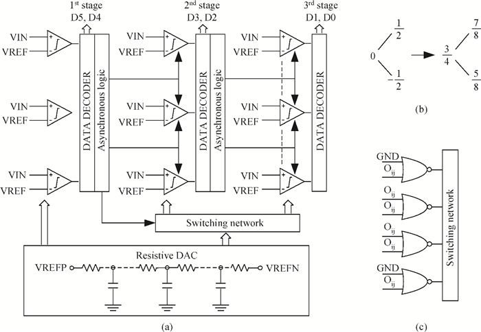
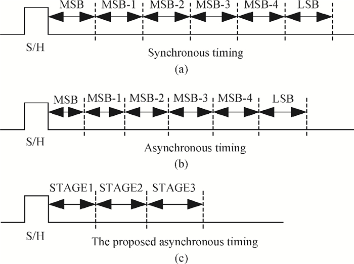
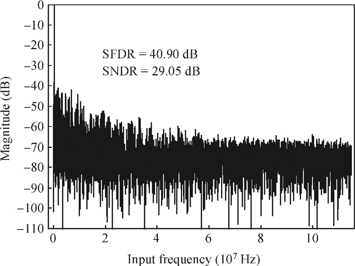
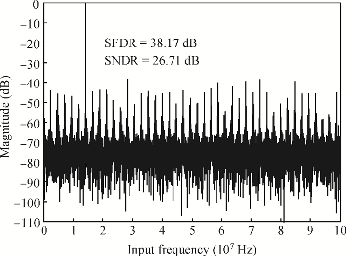
Table 1. Summary of measurement performance and comparison with several designs.

|
| [1] |
Nuzzo P, Nani C, Armiento C, et al. A 6-bit 50-MS/s threshold configuring SAR ADC in 90-nm digital CMOS. IEEE Trans Circuits Syst I, 2012, 59(1): 80 doi: 10.1109/TCSI.2011.2161368
|
| [2] |
Van Elzakker M, van Tuijl E, Geraedts P, et al. A 1.9μW 4.4 fJ/conversion-step 10 b 1 MS/s charge-redistribution ADC. IEEE ISSCC Dig Tech Papers, 2008: 244
|
| [3] |
Chen S W M, Brodersen R W. A 6 b 600 MS/s 5.3 mW asynchronous ADC in 0.13μm CMOS. IEEE J Solid-State Circuits, 2006, 41(12): 2669 doi: 10.1109/JSSC.2006.884231
|
| [4] |
Lin Y Z, Hang S J, Liu Y T, et al. An asynchronous binary-search ADC architecture with a reduced comparator count. IEEE Trans Circuits Syst I, 2010, 57(8): 1829 doi: 10.1109/TCSI.2009.2037403
|
| [5] |
Jiang T, Liu W, Zhong F Y, et al. A single-channel, 1.25-GS/s, 6-bit, 6.08-mW asynchronous successive-approximation ADC with improved feedback delay in 40-nm CMOS. IEEE J Solid-State Circuits, 2012, 47(10): 2444 doi: 10.1109/JSSC.2012.2204543
|
| [6] |
Van der Plas G, Verbruggen B. A 150 MS/s 133μW 7 b ADC in 90 nm digital CMOS using a comparator-based asynchronous binary-search sub-ADC. IEEE International Solid-State Circuits Conference (ISSCC), 2008: 242
|
| [7] |
Han Xue, Fan Hua, Wei Qi, et al. A high SFDR 6-bit 20MS/s SAR ADC based on time-domain comparator. Journal of Semiconductors, 2013, 34(8): 085008 doi: 10.1088/1674-4926/34/8/085008
|
| [8] |
Wei H, Chan C H, Chio, U F et al. An 8-b 400-MS/s 2-b-per-cycle SAR ADC with resistive DAC. IEEE J Solid-State Circuits, 2012, 47(11): 2763 doi: 10.1109/JSSC.2012.2214181
|
| [9] |
Mesgarani A, Ay S U. A single channel 6-bit 900 MS/s 2-bits per stage asynchronous binary search ADC. IEEE International Midwest Symposium on Circuit and System, 2011: 10.1109
|
| [10] |
Ye F, Cheng L, Lin K, et al. An 80-MS/s 14-bit pipelined ADC featuring 83 dB SFDR. Analog Integrated Circuit Signal Process, 2010, 63: 503 doi: 10.1007/s10470-009-9451-2
|
| [11] |
Miyahara M, Asada Y, Paik D, et al. A low-noise self-calibrating dynamic comparator for high-speed ADCs. IEEE Asian Solid-State Circuits Conference, 2008: 269 http://ieeexplore.ieee.org/document/4708780/
|
| [12] |
Figueiredo P M, Vital J C. Kickback noise reduction techniques for CMOS latched comparators. IEEE Trans Circuits Syst Ⅱ, 2006, 53(7): 541 doi: 10.1109/TCSII.2006.875308
|
| [13] |
Kobenge S. Circuit techniques for low-voltage low-power successive approximation register analog-to-digital converter. Beijing: Tsinghua University, 2010
|
| [14] |
Ginsburg B P, Chandrakasan A P. Highly interleaved 5-bit, 250 MSample/s, 1.2-mW ADC with redundant channels in 65-nm CMOS. IEEE J Solid-State Circuits, 2008, 43(12): 2641 doi: 10.1109/JSSC.2008.2006334
|
| [15] |
Cao Z, Yan S, Li Y. A 32 mW 1.25 GS/s 6 b 2 b/step SAR ADC in 0.13μm CMOS. IEEE J Solid-State Circuits, 2009, 44(3): 862 doi: 10.1109/JSSC.2008.2012329
|
| [16] |
Ginsburg B P, Chandrakasan A P. 500-MS/s 5-bit ADC in 65-nm CMOS with split capacitor array DAC. IEEE J Solid-State Circuits, 2007, 42(4): 739 doi: 10.1109/JSSC.2007.892169
|
| [17] |
Yang J, Naing T L, Brodersen R W. A 1 GS/s 6 bit 6.7 mW successive approximation ADC using asynchronous processing. IEEE J Solid-State Circuits, 2010, 45(8): 1469 doi: 10.1109/JSSC.2010.2048139
|
| [18] |
Liu Liyuan, Li Dongmei, Chen Liangdong, et al. A low power 8-bit successive approximation register A/D for a wireless body sensor node. Journal of Semiconductors, 2010, 31(6): 035002 http://www.jos.ac.cn/bdtxbcn/ch/reader/view_abstract_new.aspx?volume=31&start_page=035002
|


Article views: 3550 Times PDF downloads: 32 Times Cited by: 0 Times
Received: 17 December 2013 Revised: 19 January 2014 Online: Published: 01 July 2014
| Citation: |
Xue Han, Qi Wei, Huazhong Yang, Hui Wang. A single channel, 6-bit 230-MS/s asynchronous SAR ADC based on 2 bits/stage[J]. Journal of Semiconductors, 2014, 35(7): 075005. doi: 10.1088/1674-4926/35/7/075005
****
X Han, Q Wei, H Z Yang, H Wang. A single channel, 6-bit 230-MS/s asynchronous SAR ADC based on 2 bits/stage[J]. J. Semicond., 2014, 35(7): 075005. doi: 10.1088/1674-4926/35/7/075005.

|
| [1] |
Nuzzo P, Nani C, Armiento C, et al. A 6-bit 50-MS/s threshold configuring SAR ADC in 90-nm digital CMOS. IEEE Trans Circuits Syst I, 2012, 59(1): 80 doi: 10.1109/TCSI.2011.2161368
|
| [2] |
Van Elzakker M, van Tuijl E, Geraedts P, et al. A 1.9μW 4.4 fJ/conversion-step 10 b 1 MS/s charge-redistribution ADC. IEEE ISSCC Dig Tech Papers, 2008: 244
|
| [3] |
Chen S W M, Brodersen R W. A 6 b 600 MS/s 5.3 mW asynchronous ADC in 0.13μm CMOS. IEEE J Solid-State Circuits, 2006, 41(12): 2669 doi: 10.1109/JSSC.2006.884231
|
| [4] |
Lin Y Z, Hang S J, Liu Y T, et al. An asynchronous binary-search ADC architecture with a reduced comparator count. IEEE Trans Circuits Syst I, 2010, 57(8): 1829 doi: 10.1109/TCSI.2009.2037403
|
| [5] |
Jiang T, Liu W, Zhong F Y, et al. A single-channel, 1.25-GS/s, 6-bit, 6.08-mW asynchronous successive-approximation ADC with improved feedback delay in 40-nm CMOS. IEEE J Solid-State Circuits, 2012, 47(10): 2444 doi: 10.1109/JSSC.2012.2204543
|
| [6] |
Van der Plas G, Verbruggen B. A 150 MS/s 133μW 7 b ADC in 90 nm digital CMOS using a comparator-based asynchronous binary-search sub-ADC. IEEE International Solid-State Circuits Conference (ISSCC), 2008: 242
|
| [7] |
Han Xue, Fan Hua, Wei Qi, et al. A high SFDR 6-bit 20MS/s SAR ADC based on time-domain comparator. Journal of Semiconductors, 2013, 34(8): 085008 doi: 10.1088/1674-4926/34/8/085008
|
| [8] |
Wei H, Chan C H, Chio, U F et al. An 8-b 400-MS/s 2-b-per-cycle SAR ADC with resistive DAC. IEEE J Solid-State Circuits, 2012, 47(11): 2763 doi: 10.1109/JSSC.2012.2214181
|
| [9] |
Mesgarani A, Ay S U. A single channel 6-bit 900 MS/s 2-bits per stage asynchronous binary search ADC. IEEE International Midwest Symposium on Circuit and System, 2011: 10.1109
|
| [10] |
Ye F, Cheng L, Lin K, et al. An 80-MS/s 14-bit pipelined ADC featuring 83 dB SFDR. Analog Integrated Circuit Signal Process, 2010, 63: 503 doi: 10.1007/s10470-009-9451-2
|
| [11] |
Miyahara M, Asada Y, Paik D, et al. A low-noise self-calibrating dynamic comparator for high-speed ADCs. IEEE Asian Solid-State Circuits Conference, 2008: 269 http://ieeexplore.ieee.org/document/4708780/
|
| [12] |
Figueiredo P M, Vital J C. Kickback noise reduction techniques for CMOS latched comparators. IEEE Trans Circuits Syst Ⅱ, 2006, 53(7): 541 doi: 10.1109/TCSII.2006.875308
|
| [13] |
Kobenge S. Circuit techniques for low-voltage low-power successive approximation register analog-to-digital converter. Beijing: Tsinghua University, 2010
|
| [14] |
Ginsburg B P, Chandrakasan A P. Highly interleaved 5-bit, 250 MSample/s, 1.2-mW ADC with redundant channels in 65-nm CMOS. IEEE J Solid-State Circuits, 2008, 43(12): 2641 doi: 10.1109/JSSC.2008.2006334
|
| [15] |
Cao Z, Yan S, Li Y. A 32 mW 1.25 GS/s 6 b 2 b/step SAR ADC in 0.13μm CMOS. IEEE J Solid-State Circuits, 2009, 44(3): 862 doi: 10.1109/JSSC.2008.2012329
|
| [16] |
Ginsburg B P, Chandrakasan A P. 500-MS/s 5-bit ADC in 65-nm CMOS with split capacitor array DAC. IEEE J Solid-State Circuits, 2007, 42(4): 739 doi: 10.1109/JSSC.2007.892169
|
| [17] |
Yang J, Naing T L, Brodersen R W. A 1 GS/s 6 bit 6.7 mW successive approximation ADC using asynchronous processing. IEEE J Solid-State Circuits, 2010, 45(8): 1469 doi: 10.1109/JSSC.2010.2048139
|
| [18] |
Liu Liyuan, Li Dongmei, Chen Liangdong, et al. A low power 8-bit successive approximation register A/D for a wireless body sensor node. Journal of Semiconductors, 2010, 31(6): 035002 http://www.jos.ac.cn/bdtxbcn/ch/reader/view_abstract_new.aspx?volume=31&start_page=035002
|

 WeChat ID
Journal of Semiconductors © 2017 All Rights Reserved 京ICP备05085259号-2

 DownLoad: