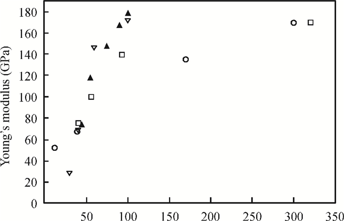
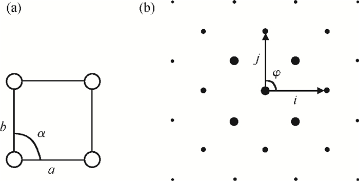
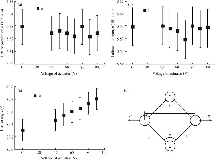
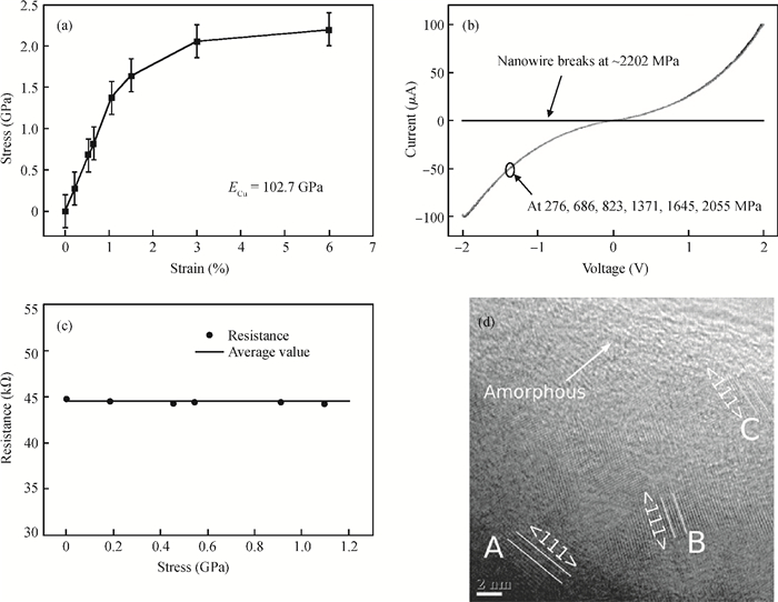
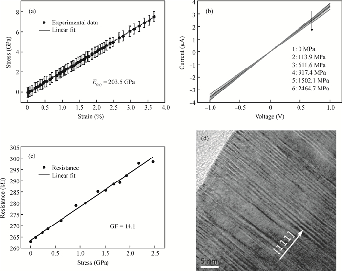
| [1] |
Namazu T, Isono Y, Tanaka T. Evaluation of size effect on mechanical properties of single crystal silicon by nanoscale bending test using AFM. J Microelectromech Syst, 2000, 9:450 doi: 10.1109/84.896765 |
| [2] |
|
| [3] |
Li D, Wu Y, Kim P, et al. Thermal conductivity of individual silicon nanowires. Appl Phys Lett, 2003, 83:2934 doi: 10.1063/1.1616981 |
| [4] |
He R, Yang P. Giant piezoresistance effect in silicon nanowires. Nature Nanotechnol, 2006, 1:42 doi: 10.1038/nnano.2006.53 |
| [5] |
Ma D D D, Lee C S, Au F C K, et al. Small-diameter silicon nanowire surfaces. Science, 2003, 299:1874 doi: 10.1126/science.1080313 |
| [6] |
Bell D J, Lu T J, Fleck N A, et al. MEMS actuators and sensors:observations on their performance and selection for purpose. J Micromech Microeng, 2005, 15:S153 doi: 10.1088/0960-1317/15/7/022 |
| [7] |
Kiuchi M, Matsui S, Isono Y. Mechanical characteristics of FIB deposited carbon nanowires using an electrostatic actuated nano tensile testing device. J Microelectromech Syst, 2007, 16:191 doi: 10.1109/JMEMS.2006.889663 |
| [8] |
|
| [9] |
Han J H, Saif M T. In situ microtensile stage for electromechanical characterization of nanoscale freestanding films. Rev Sci Instrum, 2006, 77:045102 doi: 10.1063/1.2188368 |
| [10] |
Zhu Y, Espinosa H D. An electromechanical material testing system for in situ electron microscopy and applications. P Natl Acad Sci USA, 2005, 102:14503 doi: 10.1073/pnas.0506544102 |
| [11] |
Zhu Y, Ke C, Espinosa H D. Experimental techniques for the mechanical characterization of one-dimensional nanostructures. Exp Mech, 2007, 47:7 doi: 10.1007/s11340-006-0406-6 |
| [12] |
Peng B, Locascio M, Zapol P, et al. Measurements of near-ultimate strength for multiwalled carbon nanotubes and irradiation-induced crosslinking improvements. Nature Nanotechnol, 2008, 3:626 doi: 10.1038/nnano.2008.211 |
| [13] |
Zhang D, Breguet J M, Clavel R, et al. In situ electron microscopy mechanical testing of silicon nanowires using electrostatically actuated tensile stages. J Microelectromech Syst, 2010, 19:663 doi: 10.1109/JMEMS.2010.2044746 |
| [14] |
Zhang D, Drissen W, Breguet J M, et al. A high-sensitivity and quasi-linear capacitive sensor for nanomechanical testing applications. J Micromech Microeng, 2009, 19:075003 doi: 10.1088/0960-1317/19/7/075003 |
| [15] |
|
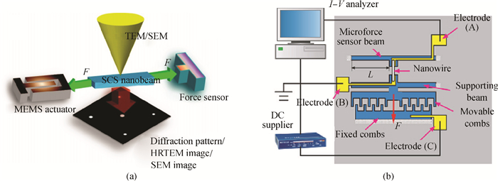
| [16] |
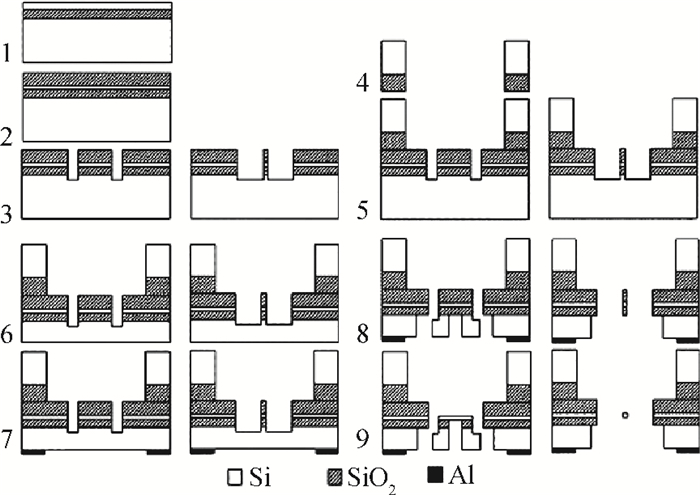
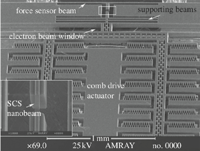
Jin Q, Wang Y, Li T, et al. A MEMS device for in-situ TEM test of SCS nanobeam. Sci China Ser E Technol Sci, 2008, 51:1491 doi: 10.1007/s11431-008-0123-8 |
| [17] |
|
| [18] |
|
| [19] |
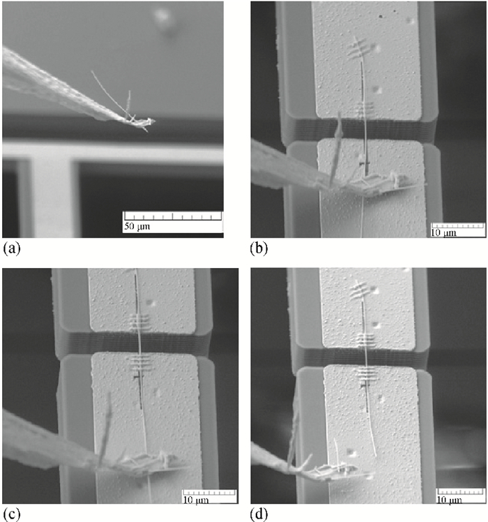
Jin Q, Li T, Wang Y, et al. Confirmation on the size-dependence of Young's modulus of single crystal silicon from the TEM tensile tests. Proc IEEE Sensors, Hawaii, USA, 2010:2530 http://ieeexplore.ieee.org/document/5690465/ |
| [20] |
|
| [21] |
Li X, Ono T, Wang Y L, et al. Ultrathin single crystalline-silicon cantilever resonators:fabrication technology and significant specimen size effect on Young's modulus. Appl Phys Lett, 2003, 83:3081 doi: 10.1063/1.1618369 |
| [22] |
Sadeghian H, Yang C K, Goosen J F L, et al. Characterizing size-dependent effective elastic modulus of silicon nanocantilevers using electrostatic pull-in instability. Appl Phys Lett, 2009, 94:221903 doi: 10.1063/1.3148774 |
| [23] |
Bartenwerfer M, Fatikow S, Zeng H, et al. Individual nanowire handling for NEMS fabrication. IEEE/ASME Int Conf on Advanced Intelligent Mechatronics, Kaohsiung, Taiwan, 2012:562 http://ieeexplore.ieee.org/document/6266052/ |
| [24] |
Cao A, Wei Y, Ma E. Grain boundary effects on plastic deformation and fracture mechanisms in Cu nanowires:molecular dynamics simulations. Phys Rev B, 2008, 77:195429 doi: 10.1103/PhysRevB.77.195429 |
| [25] |
Cao H, Wang L, Qiu Y, et al. Synthesis and I-V properties of aligned copper nanowires. Nanotechnology, 2006, 17:1736 doi: 10.1088/0957-4484/17/6/032 |
| [26] |
John C, Kenneth J. Physics. 4th ed. New York:Wiley, 1998:755
|
| [27] |
Huang Q, Lilley C M, Bode M, et al. Electrical failure analysis of Au nanowires. 8th IEEE Conf on Nanotechnology, Arlington, TX, 2008:549
|
| [28] |
Perisanu S, Gouttenoire V, Vincent P, et al. Mechanical properties of SiC nanowires determined by scanning electron and field emission microscopies. Phys Rev B, 2008, 77:165434 doi: 10.1103/PhysRevB.77.165434 |
| [29] |
Petrovic J J, Milewski J V, Rohr D L, et al. Tensile mechanical-properties of SiC whiskers. J Mater Sci, 1985, 20:1167 doi: 10.1007/BF01026310 |
| [30] |
Wang J, Lu C, Wang Q, et al. Understanding large plastic deformation of SiC nanowires at room temperature. Europhys Lett, 2011, 95:63003 doi: 10.1209/0295-5075/95/63003 |
| [31] |
|
| [32] |
Mukherjee M. Silicon carbide-materials, processing and applications in electronic devices. Rijeka:In Tech, 2011:369
|
| [33] |
Shor J S, Bemis L, Kurtz A D. Characterization of monolithic n-type 6H-SiC piezoresistive sensing elements. IEEE Trans Electron Devices, 1994, 41:661 doi: 10.1109/16.285013 |


 DownLoad: