


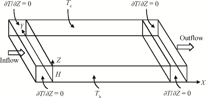
Fig. 1.
Sketch of horizontal reactors.
SEMICONDUCTOR MATERIALS
Jiaxing Wei, Rui Xu, Yanfei Yu, Jinliang Hou and Changfeng Li
Corresponding author: Li Changfeng, Email:cfli@ujs.edu.cn
Abstract: Numerical simulation, based on simple reaction models that manifest the deposition quality of silicon from silane, was undertaken to investigate the horizontal reactor, with longitudinal and transversal aspect ratios of 10 and 4, respectively. The effects of Rayleigh (Ra) and Reynolds (Re) numbers on the Si deposition rate in these turbulent-type reactors are discussed. The results show that the time-averaged deposition rate is fairly uniform and fast, although the instantaneous deposition is non-uniform in these turbulent reactors. In addition, the increase of the Re number within a certain range can compensate for the path loss of the reactant and obviously enhance the downstream deposition rate, but deteriorate the transverse distribution of the deposition.
Keywords: chemical vapor deposition, turbulence, deposition rate, natural convection
| [1] |
Manasevit H M. Single-crystal gallium arsenide on insulating substrates. Appl Phys Lett, 1968, 12:156 doi: 10.1063/1.1651934
|
| [2] |
Zuo R, Li H. The optimum transport processes and design of MOCVD reactor. Journal of Semiconductors, 2008, 29(6):1164 http://www.jos.ac.cn/bdtxbcn/ch/reader/view_abstract.aspx?file_no=07101601&flag=1
|
| [3] |
Kelly R E. The onset and development of thermal convection in fully developed shear flow. Adv Appl Mechan, 1994, 31:35 doi: 10.1016/S0065-2156(08)70255-2
|
| [4] |
Nicolas X, Benzaoui A, Xin S. Numerical simulation of thermoconvective flows and more uniform depositions in a cold wall rectangular APCVD reactor. J Cryst Growth, 2008, 310:174 doi: 10.1016/j.jcrysgro.2007.10.016
|
| [5] |
Giling L J. Crystal growth of electronic materials. North-Holland Amsterdam: Emanuel Kaldis (Editor), 1985
|
| [6] |
Santrn H V, Kleun C R, Van Den Akker H E A. On turbulent flows in cold-wall CVD reactors. J Cryst Growth, 2000, 212:299 doi: 10.1016/S0022-0248(00)00033-6
|
| [7] |
Tian Y, Li C F, Jiang H H, et al. Numerical simulation on turbulence flows in vertical chemical vapor deposition reactors. J Cryst Growth, 2011, 318:168 doi: 10.1016/j.jcrysgro.2010.11.070
|
| [8] |
Liu S B, Li H, Guo F J, et al. Exploration of thermal characteristics in turbulent horizontal APCVD reactors. J Synthetic Crystals, 2013, 42(5):901
|
| [9] |
FLUENT Users Guide. Fluent Inc, 2003
|
| [10] |
Shih T H, Liou W W, Shabbir A, et al. A new eddy viscosity model for high Reynolds number turbulent flows. Computers Fluids, 1995, 24(3):227 doi: 10.1016/0045-7930(94)00032-T
|
| [11] |
Heslot F, Castaing B, Libchaber A. Transition to turbulence in helium gas. Phys Rev A, 1987, 36:5870 doi: 10.1103/PhysRevA.36.5870
|
| [12] |
Lin T F. Buoyancy driven vortex flow and thermal structure in a very low Reynolds number mixed convective gas flow through a horizontal channel. International Journal of Heat and Fluid Flow, 2003, 24:299 doi: 10.1016/S0142-727X(03)00020-1
|
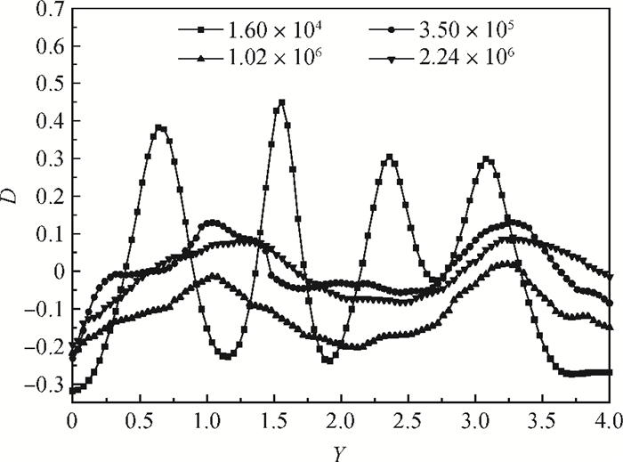
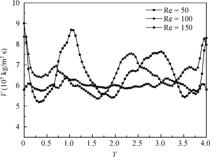
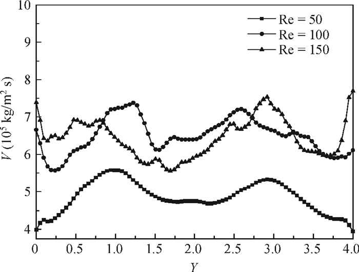
Table 1. The meshing and average deposition rates.

|
Table 2. The average deposition rate of the substrate vm.

|
| [1] |
Manasevit H M. Single-crystal gallium arsenide on insulating substrates. Appl Phys Lett, 1968, 12:156 doi: 10.1063/1.1651934
|
| [2] |
Zuo R, Li H. The optimum transport processes and design of MOCVD reactor. Journal of Semiconductors, 2008, 29(6):1164 http://www.jos.ac.cn/bdtxbcn/ch/reader/view_abstract.aspx?file_no=07101601&flag=1
|
| [3] |
Kelly R E. The onset and development of thermal convection in fully developed shear flow. Adv Appl Mechan, 1994, 31:35 doi: 10.1016/S0065-2156(08)70255-2
|
| [4] |
Nicolas X, Benzaoui A, Xin S. Numerical simulation of thermoconvective flows and more uniform depositions in a cold wall rectangular APCVD reactor. J Cryst Growth, 2008, 310:174 doi: 10.1016/j.jcrysgro.2007.10.016
|
| [5] |
Giling L J. Crystal growth of electronic materials. North-Holland Amsterdam: Emanuel Kaldis (Editor), 1985
|
| [6] |
Santrn H V, Kleun C R, Van Den Akker H E A. On turbulent flows in cold-wall CVD reactors. J Cryst Growth, 2000, 212:299 doi: 10.1016/S0022-0248(00)00033-6
|
| [7] |
Tian Y, Li C F, Jiang H H, et al. Numerical simulation on turbulence flows in vertical chemical vapor deposition reactors. J Cryst Growth, 2011, 318:168 doi: 10.1016/j.jcrysgro.2010.11.070
|
| [8] |
Liu S B, Li H, Guo F J, et al. Exploration of thermal characteristics in turbulent horizontal APCVD reactors. J Synthetic Crystals, 2013, 42(5):901
|
| [9] |
FLUENT Users Guide. Fluent Inc, 2003
|
| [10] |
Shih T H, Liou W W, Shabbir A, et al. A new eddy viscosity model for high Reynolds number turbulent flows. Computers Fluids, 1995, 24(3):227 doi: 10.1016/0045-7930(94)00032-T
|
| [11] |
Heslot F, Castaing B, Libchaber A. Transition to turbulence in helium gas. Phys Rev A, 1987, 36:5870 doi: 10.1103/PhysRevA.36.5870
|
| [12] |
Lin T F. Buoyancy driven vortex flow and thermal structure in a very low Reynolds number mixed convective gas flow through a horizontal channel. International Journal of Heat and Fluid Flow, 2003, 24:299 doi: 10.1016/S0142-727X(03)00020-1
|


Article views: 3188 Times PDF downloads: 30 Times Cited by: 0 Times
Received: 26 December 2013 Revised: 19 March 2014 Online: Published: 01 August 2014
| Citation: |
Jiaxing Wei, Rui Xu, Yanfei Yu, Jinliang Hou, Changfeng Li. Simulation and analysis of Si deposition in turbulent CVD reactors[J]. Journal of Semiconductors, 2014, 35(8): 083002. doi: 10.1088/1674-4926/35/8/083002
****
J X Wei, R Xu, Y F Yu, J L Hou, C F Li. Simulation and analysis of Si deposition in turbulent CVD reactors[J]. J. Semicond., 2014, 35(8): 083002. doi: 10.1088/1674-4926/35/8/083002.

|
| [1] |
Manasevit H M. Single-crystal gallium arsenide on insulating substrates. Appl Phys Lett, 1968, 12:156 doi: 10.1063/1.1651934
|
| [2] |
Zuo R, Li H. The optimum transport processes and design of MOCVD reactor. Journal of Semiconductors, 2008, 29(6):1164 http://www.jos.ac.cn/bdtxbcn/ch/reader/view_abstract.aspx?file_no=07101601&flag=1
|
| [3] |
Kelly R E. The onset and development of thermal convection in fully developed shear flow. Adv Appl Mechan, 1994, 31:35 doi: 10.1016/S0065-2156(08)70255-2
|
| [4] |
Nicolas X, Benzaoui A, Xin S. Numerical simulation of thermoconvective flows and more uniform depositions in a cold wall rectangular APCVD reactor. J Cryst Growth, 2008, 310:174 doi: 10.1016/j.jcrysgro.2007.10.016
|
| [5] |
Giling L J. Crystal growth of electronic materials. North-Holland Amsterdam: Emanuel Kaldis (Editor), 1985
|
| [6] |
Santrn H V, Kleun C R, Van Den Akker H E A. On turbulent flows in cold-wall CVD reactors. J Cryst Growth, 2000, 212:299 doi: 10.1016/S0022-0248(00)00033-6
|
| [7] |
Tian Y, Li C F, Jiang H H, et al. Numerical simulation on turbulence flows in vertical chemical vapor deposition reactors. J Cryst Growth, 2011, 318:168 doi: 10.1016/j.jcrysgro.2010.11.070
|
| [8] |
Liu S B, Li H, Guo F J, et al. Exploration of thermal characteristics in turbulent horizontal APCVD reactors. J Synthetic Crystals, 2013, 42(5):901
|
| [9] |
FLUENT Users Guide. Fluent Inc, 2003
|
| [10] |
Shih T H, Liou W W, Shabbir A, et al. A new eddy viscosity model for high Reynolds number turbulent flows. Computers Fluids, 1995, 24(3):227 doi: 10.1016/0045-7930(94)00032-T
|
| [11] |
Heslot F, Castaing B, Libchaber A. Transition to turbulence in helium gas. Phys Rev A, 1987, 36:5870 doi: 10.1103/PhysRevA.36.5870
|
| [12] |
Lin T F. Buoyancy driven vortex flow and thermal structure in a very low Reynolds number mixed convective gas flow through a horizontal channel. International Journal of Heat and Fluid Flow, 2003, 24:299 doi: 10.1016/S0142-727X(03)00020-1
|

 WeChat ID
Journal of Semiconductors © 2017 All Rights Reserved 京ICP备05085259号-2

 DownLoad:

