


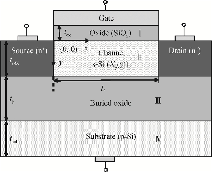
Fig. 1.
Schematic diagram of an SSOI MOSFET.
SEMICONDUCTOR DEVICES
Gopal Rawat1, , Sanjay Kumar1, Ekta Goel1, Mirgender Kumar1, Sarvesh Dubey2 and S. Jit1
Corresponding author: Gopal Rawat, Email:gopal.rawat.ece11@iitbhu.ac.in
Abstract: This paper presents the analytical modeling of subthreshold current and subthreshold swing of short-channel fully-depleted (FD) strained-Si-on-insulator (SSOI) MOSFETs having vertical Gaussian-like doping profile in the channel. The subthreshold current and subthreshold swing have been derived using the parabolic approximation method. In addition to the effect of strain on silicon layer, various other device parameters such as channel length (L), gate-oxide thickness (tox), strained-Si channel thickness (ts-Si), peak doping concentration (NP), project range (Rp) and straggle (σp) of the Gaussian profile have been considered while predicting the device characteristics. The present work may help to overcome the degradation in subthreshold characteristics with strain engineering. These subthreshold current and swing models provide valuable information for strained-Si MOSFET design. Accuracy of the proposed models is verified using the commercially available ATLASTM, a two-dimensional (2D) device simulator from SILVACO.
Keywords: strained-Si-on-insulator (SSOI), Poisson's solution, short-channel-effects
| [1] |
Welser J, Hoyt J L, Gibbons J F. Electron mobility enhancement in strained-Si n type metal-oxide-semiconductor field-effect transistors. IEEE Electron Device Lett, 1994, 15(3):100 doi: 10.1109/55.285389
|
| [2] |
Badcock S G, O'Neill A G, Chester E G. Device and circuit performance of SiGe/Si MOSFETs. Solid-State Electron, 2002, 46(11):1925 doi: 10.1016/S0038-1101(02)00131-4
|
| [3] |
ITRS, International Technology Roadmap for Semiconductor. Austin: Semiconductor Industry Assoc. , 2001
|
| [4] |
Mahato S S, Chakraborty P, Maiti T K, et al. DIBL in short-channel strained-Si n-MOSFET. IEEE Proceedings 15th International Symposium on the Physical and Failure Analysis of Integrated Circuits (IPFA), Singapore, 2008: 1 http://ieeexplore.ieee.org/xpls/abs_all.jsp?arnumber=4588186
|
| [5] |
Kumar M J, Venkataraman V, Nawal S. A simple analytical threshold voltage model of nanoscale single-layer fully depleted strained-silicon-on-insulator MOSFETs. IEEE Trans Electron Devices, 2006, 53(10):2500 doi: 10.1109/TED.2006.882041
|
| [6] |
Gamiz F, Cassinello P C, Roldan J B, et al. Electron transport in strained Si inversion layers grown on SiGe-on-insulator substrates. J Appl Phys, 2002, 92(1):288 doi: 10.1063/1.1481962
|
| [7] |
Onsongo D, Kelly D Q, Dey S, et al. Improved hot-electron reliability in strained-Si nMOS. IEEE Trans Electron Devices, 2004, 51(12):2193 doi: 10.1109/TED.2004.839871
|
| [8] |
Horiguchi M, Sakata T, Itoh K. Switched-source-impedance CMOS circuit for low standby subthreshold current giga-scale LSI's. IEEE J Solid-State Circuits, 1993, 28(11):1131 doi: 10.1109/4.245593
|
| [9] |
Ieong M, Doris B, Kedzierski J, et al. Silicon device scaling to the sub-10-nm regime. Science, 2004, 306(5704):2057 doi: 10.1126/science.1100731
|
| [10] |
Kumar M, Dubey S, Tiwari P K, et al. Analytical modeling and simulation of subthreshold characteristics of back-gated SSGOI and SSOI MOSFETs:a comparative study. Current Applied Physics, 2013, 13(8):1778 doi: 10.1016/j.cap.2013.07.013
|
| [11] |
Laker K R, Sansen W M C. Design of analog integrated circuits and systems. New York:McGraw-Hill, 1994
|
| [12] |
Mead C, Ismail M. Analog VLSI and neural systems. Springer, 1989 http://dl.acm.org/citation.cfm?id=64998
|
| [13] |
Aghtar S, Haslett J W, Trofimenkoff F N. Subthreshold analysis of an MOS analog switch. IEEE Trans Electron Devices, 1997, 44(1):89 doi: 10.1109/16.554798
|
| [14] |
Maiti T K, Banerjee A, Maiti C K. An explicit surface-potential based biaxial strained-Si n-MOSFET model for circuit simulation. Engineering, 2010, 2(11):879 doi: 10.4236/eng.2010.211111
|
| [15] |
Mukhopadhyay B, Biswas A, Basu P K, et al. Modelling of threshold voltage and subthreshold slope of strained-Si MOSFETs including quantum effects. Semicond Sci Technol, 2008, 23(9):095017 doi: 10.1088/0268-1242/23/9/095017
|
| [16] |
Kumar M, Dubey S, Tiwari P K, et al. An analytical modeling of interface charge induced effects on subthreshold current and subthreshold swing of strained-Si (s-Si) on silicon-germinium-on-insulator (SGOI) MOSFETs. 5th International Conference on Computers and Devices for Communication (CODEC), Kolkata, India, 2012: 1
|
| [17] |
Qin S, Zhang H, Hu H, et al. A two-dimensional subthreshold current model for strained-Si MOSFET. Science China Physics, Mechanics and Astronomy, 2011, 54(12):2181 doi: 10.1007/s11433-011-4501-z
|
| [18] |
Kumar M, Dubey S, Tiwari P K, et al. Analytical models of subthreshold current and swing of short-channel strained-Si (s-Si) on silicon-germanium-on-insulator (SGOI) MOSFETs. Superlattices and Microstructures, 2013, 58:1 doi: 10.1016/j.spmi.2013.02.012
|
| [19] |
Kumar M J, Venkataraman V, Nawal S. Comprehensive approach to modeling threshold voltage of nanoscale strained silicon SOI MOSFETs. Journal of Computational Electronics, 2007, 6(4):439 doi: 10.1007/s10825-007-0153-7
|
| [20] |
Kumar M, Dubey S, Tiwari P K, et al. A 2D analytical modeling approach for nanoscale strained-Si (s-Si) on silicon-germanium-on-insulator (SGOI) MOSFETs by evanescent mode analysis. IEEE Proceedings of International Conference on Communications, Devices and Intelligent Systems (CODIS), Kolkata, India, 2012: 449 http://ieeexplore.ieee.org/document/6422235/
|
| [21] |
Dasgupta A, Lahiri S K. A two-dimensional analytical model of threshold voltages of short-channel MOSFETs with Gaussian-doped channels. IEEE Trans Electron Devices, 1988, 35(3):390 doi: 10.1109/16.2468
|
| [22] |
Dubey S, Tiwari P K, Jit S. A two-dimensional model for the subthreshold swing of short-channel double-gate metal-oxide-semiconductor field effect transistors with a vertical Gaussian-like doping profile. J Appl Phys, 2011, 109(5):054508 doi: 10.1063/1.3552309
|
| [23] |
Zhang G, Shao Z, Zhou K. Threshold voltage model of short-channel FD-SOI MOSFETs with vertical Gaussian profile. IEEE Trans Electron Devices, 2008, 55(3):803 doi: 10.1109/TED.2007.914832
|
| [24] |
ATLAS manual: Silvaco Int. Santa Clara, 2008
|
| [25] |
Zhang W, Fossum J G. On the threshold voltage of strained-Si-Si1-xGex MOSFETs. IEEE Trans Electron Devices, 2005, 52(2):263 doi: 10.1109/TED.2004.842716
|
| [26] |
Trivedi V P, Fossum J G. Scaling fully depleted SOI CMOS. IEEE Trans Electron Devices, 2003, 50(10):2095 doi: 10.1109/TED.2003.816915
|
| [27] |
Dey A, Chakravorty A, Dasgupta, et al. Analytical model of subthreshold current and slope for asymmetric 4-T and 3-T double-gate MOSFETs. IEEE Trans Electron Devices, 2008, 55(12):3442 doi: 10.1109/TED.2008.2006109
|
| [28] |
Kumar M, Dubey S, Tiwari P K, et al. Two-dimensional modeling of subthreshold current and subthreshold swing of double-material-gate (DMG) strained-Si (s-Si) on SGOI MOSFETs. Journal of Computational Electronics, 2013, 12(2):275 doi: 10.1007/s10825-013-0442-2
|
| [29] |
Jankovic N D, Armstrong G A. Comparative analysis of the DC performance of DG MOSFETs on highly-doped and near-intrinsic silicon layers. Microelectron J, 2004, 35(8):647 doi: 10.1016/j.mejo.2004.04.007
|


Article views: 3350 Times PDF downloads: 37 Times Cited by: 0 Times
Received: 14 January 2014 Revised: 25 February 2014 Online: Published: 01 August 2014
| Citation: |
Gopal Rawat, Sanjay Kumar, Ekta Goel, Mirgender Kumar, Sarvesh Dubey, S. Jit. Analytical modeling of subthreshold current and subthreshold swing of Gaussian-doped strained-Si-on-insulator MOSFETs[J]. Journal of Semiconductors, 2014, 35(8): 084001. doi: 10.1088/1674-4926/35/8/084001
****
G Rawat, S Kumar, E Goel, M Kumar, S Dubey, S. Jit. Analytical modeling of subthreshold current and subthreshold swing of Gaussian-doped strained-Si-on-insulator MOSFETs[J]. J. Semicond., 2014, 35(8): 084001. doi: 10.1088/1674-4926/35/8/084001.

|
| [1] |
Welser J, Hoyt J L, Gibbons J F. Electron mobility enhancement in strained-Si n type metal-oxide-semiconductor field-effect transistors. IEEE Electron Device Lett, 1994, 15(3):100 doi: 10.1109/55.285389
|
| [2] |
Badcock S G, O'Neill A G, Chester E G. Device and circuit performance of SiGe/Si MOSFETs. Solid-State Electron, 2002, 46(11):1925 doi: 10.1016/S0038-1101(02)00131-4
|
| [3] |
ITRS, International Technology Roadmap for Semiconductor. Austin: Semiconductor Industry Assoc. , 2001
|
| [4] |
Mahato S S, Chakraborty P, Maiti T K, et al. DIBL in short-channel strained-Si n-MOSFET. IEEE Proceedings 15th International Symposium on the Physical and Failure Analysis of Integrated Circuits (IPFA), Singapore, 2008: 1 http://ieeexplore.ieee.org/xpls/abs_all.jsp?arnumber=4588186
|
| [5] |
Kumar M J, Venkataraman V, Nawal S. A simple analytical threshold voltage model of nanoscale single-layer fully depleted strained-silicon-on-insulator MOSFETs. IEEE Trans Electron Devices, 2006, 53(10):2500 doi: 10.1109/TED.2006.882041
|
| [6] |
Gamiz F, Cassinello P C, Roldan J B, et al. Electron transport in strained Si inversion layers grown on SiGe-on-insulator substrates. J Appl Phys, 2002, 92(1):288 doi: 10.1063/1.1481962
|
| [7] |
Onsongo D, Kelly D Q, Dey S, et al. Improved hot-electron reliability in strained-Si nMOS. IEEE Trans Electron Devices, 2004, 51(12):2193 doi: 10.1109/TED.2004.839871
|
| [8] |
Horiguchi M, Sakata T, Itoh K. Switched-source-impedance CMOS circuit for low standby subthreshold current giga-scale LSI's. IEEE J Solid-State Circuits, 1993, 28(11):1131 doi: 10.1109/4.245593
|
| [9] |
Ieong M, Doris B, Kedzierski J, et al. Silicon device scaling to the sub-10-nm regime. Science, 2004, 306(5704):2057 doi: 10.1126/science.1100731
|
| [10] |
Kumar M, Dubey S, Tiwari P K, et al. Analytical modeling and simulation of subthreshold characteristics of back-gated SSGOI and SSOI MOSFETs:a comparative study. Current Applied Physics, 2013, 13(8):1778 doi: 10.1016/j.cap.2013.07.013
|
| [11] |
Laker K R, Sansen W M C. Design of analog integrated circuits and systems. New York:McGraw-Hill, 1994
|
| [12] |
Mead C, Ismail M. Analog VLSI and neural systems. Springer, 1989 http://dl.acm.org/citation.cfm?id=64998
|
| [13] |
Aghtar S, Haslett J W, Trofimenkoff F N. Subthreshold analysis of an MOS analog switch. IEEE Trans Electron Devices, 1997, 44(1):89 doi: 10.1109/16.554798
|
| [14] |
Maiti T K, Banerjee A, Maiti C K. An explicit surface-potential based biaxial strained-Si n-MOSFET model for circuit simulation. Engineering, 2010, 2(11):879 doi: 10.4236/eng.2010.211111
|
| [15] |
Mukhopadhyay B, Biswas A, Basu P K, et al. Modelling of threshold voltage and subthreshold slope of strained-Si MOSFETs including quantum effects. Semicond Sci Technol, 2008, 23(9):095017 doi: 10.1088/0268-1242/23/9/095017
|
| [16] |
Kumar M, Dubey S, Tiwari P K, et al. An analytical modeling of interface charge induced effects on subthreshold current and subthreshold swing of strained-Si (s-Si) on silicon-germinium-on-insulator (SGOI) MOSFETs. 5th International Conference on Computers and Devices for Communication (CODEC), Kolkata, India, 2012: 1
|
| [17] |
Qin S, Zhang H, Hu H, et al. A two-dimensional subthreshold current model for strained-Si MOSFET. Science China Physics, Mechanics and Astronomy, 2011, 54(12):2181 doi: 10.1007/s11433-011-4501-z
|
| [18] |
Kumar M, Dubey S, Tiwari P K, et al. Analytical models of subthreshold current and swing of short-channel strained-Si (s-Si) on silicon-germanium-on-insulator (SGOI) MOSFETs. Superlattices and Microstructures, 2013, 58:1 doi: 10.1016/j.spmi.2013.02.012
|
| [19] |
Kumar M J, Venkataraman V, Nawal S. Comprehensive approach to modeling threshold voltage of nanoscale strained silicon SOI MOSFETs. Journal of Computational Electronics, 2007, 6(4):439 doi: 10.1007/s10825-007-0153-7
|
| [20] |
Kumar M, Dubey S, Tiwari P K, et al. A 2D analytical modeling approach for nanoscale strained-Si (s-Si) on silicon-germanium-on-insulator (SGOI) MOSFETs by evanescent mode analysis. IEEE Proceedings of International Conference on Communications, Devices and Intelligent Systems (CODIS), Kolkata, India, 2012: 449 http://ieeexplore.ieee.org/document/6422235/
|
| [21] |
Dasgupta A, Lahiri S K. A two-dimensional analytical model of threshold voltages of short-channel MOSFETs with Gaussian-doped channels. IEEE Trans Electron Devices, 1988, 35(3):390 doi: 10.1109/16.2468
|
| [22] |
Dubey S, Tiwari P K, Jit S. A two-dimensional model for the subthreshold swing of short-channel double-gate metal-oxide-semiconductor field effect transistors with a vertical Gaussian-like doping profile. J Appl Phys, 2011, 109(5):054508 doi: 10.1063/1.3552309
|
| [23] |
Zhang G, Shao Z, Zhou K. Threshold voltage model of short-channel FD-SOI MOSFETs with vertical Gaussian profile. IEEE Trans Electron Devices, 2008, 55(3):803 doi: 10.1109/TED.2007.914832
|
| [24] |
ATLAS manual: Silvaco Int. Santa Clara, 2008
|
| [25] |
Zhang W, Fossum J G. On the threshold voltage of strained-Si-Si1-xGex MOSFETs. IEEE Trans Electron Devices, 2005, 52(2):263 doi: 10.1109/TED.2004.842716
|
| [26] |
Trivedi V P, Fossum J G. Scaling fully depleted SOI CMOS. IEEE Trans Electron Devices, 2003, 50(10):2095 doi: 10.1109/TED.2003.816915
|
| [27] |
Dey A, Chakravorty A, Dasgupta, et al. Analytical model of subthreshold current and slope for asymmetric 4-T and 3-T double-gate MOSFETs. IEEE Trans Electron Devices, 2008, 55(12):3442 doi: 10.1109/TED.2008.2006109
|
| [28] |
Kumar M, Dubey S, Tiwari P K, et al. Two-dimensional modeling of subthreshold current and subthreshold swing of double-material-gate (DMG) strained-Si (s-Si) on SGOI MOSFETs. Journal of Computational Electronics, 2013, 12(2):275 doi: 10.1007/s10825-013-0442-2
|
| [29] |
Jankovic N D, Armstrong G A. Comparative analysis of the DC performance of DG MOSFETs on highly-doped and near-intrinsic silicon layers. Microelectron J, 2004, 35(8):647 doi: 10.1016/j.mejo.2004.04.007
|

 WeChat ID
Journal of Semiconductors © 2017 All Rights Reserved 京ICP备05085259号-2

 DownLoad:

