


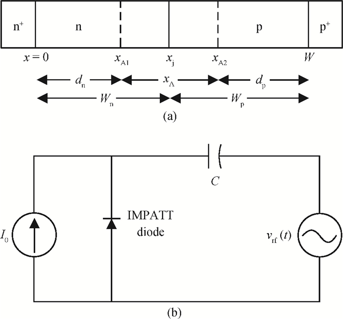
Fig. 1.
(a) 1-D model of DDR IMPATT device, (b) voltage driven IMPATT diode oscillator and associated circuit.
SEMICONDUCTOR DEVICES
Aritra Acharyya1, , Aliva Mallik2, Debopriya Banerjee2, Suman Ganguli2, Arindam Das2, Sudeepto Dasgupta2 and J.P. Banerjee1
Corresponding author: Aritra Acharyya, Email:ari_besu@yahoo.co.in
Abstract: Large-signal (L-S) characterizations of double-drift region (DDR) impact avalanche transit time (IMPATT) devices based on group Ⅲ-Ⅴ semiconductors such as wurtzite (Wz) GaN, GaAs and InP have been carried out at both millimeter-wave (mm-wave) and terahertz (THz) frequency bands. A L-S simulation technique based on a non-sinusoidal voltage excitation (NSVE) model developed by the authors has been used to obtain the high frequency properties of the above mentioned devices. The effect of band-to-band tunneling on the L-S properties of the device at different mm-wave and THz frequencies are also investigated. Similar studies are also carried out for DDR IMPATTs based on the most popular semiconductor material, i.e. Si, for the sake of comparison. A comparative study of the devices based on conventional semiconductor materials (i.e. GaAs, InP and Si) with those based on Wz-GaN shows significantly better performance capabilities of the latter at both mm-wave and THz frequencies.
Keywords: DDR IMPATTs, GaN, group Ⅲ-Ⅴ, large-signal simulation, millimeter-wave, terahertz regime, wurtzite
| [1] |
Midford T A, Bernick R L. Millimeter wave CW IMPATT diodes and oscillators. IEEE Trans Microw Theory Tech, 1979, 27:483 doi: 10.1109/TMTT.1979.1129653
|
| [2] |
Luy J F, Casel A, Behr W, et al. A 90-GHz double-drift IMPATT diode made with Si MBE. IEEE Trans Electron Devices, 1987, 34:1084 doi: 10.1109/T-ED.1987.23049
|
| [3] |
Wollitzer M, Buchler J, Schafflr F, et al. D-band Si-IMPATT diodes with 300 mW CW output power at 140 GHz. Electron Lett, 1996, 32:122 doi: 10.1049/el:19960088
|
| [4] |
Adlerstein M G, Chu S L G. GaAs IMPATT diodes for 60 GHz. IEEE Electron Devices Lett, 1984, 5:97 doi: 10.1109/EDL.1984.25844
|
| [5] |
Eisele H. Selective etching technology for 94 GHz, GaAs IMPATT diodes on diamond heat sinks. Solid-State Electron, 1989, 32(3):253 doi: 10.1016/0038-1101(89)90100-7
|
| [6] |
Tschernitz M, Freyer J. 140 GHz GaAs double-read IMPATT diodes. Electron Lett, 1995, 31(7):582 doi: 10.1049/el:19950390
|
| [7] |
Eisele H, Chen C C, Munns G O, et al. The potential of InP IMPATT diodes as high-power millimeter-wave sources:first experimental results. IEEE MTT-S International Microwave Symposium Digest, 1996, 2:529 http://ieeexplore.ieee.org/xpls/abs_all.jsp?arnumber=510989
|
| [8] |
Trew R J, Yan J B, Mock P M. The potentiality of diamond and SiC electronic devices for microwave and millimeter-wave power applications. Proc IEEE, 1991, 79(5):598 doi: 10.1109/5.90128
|
| [9] |
Mock P M, Trew R J. RF performance characteristics of double-drift MM-wave diamond IMPATT diodes. Proc IEEE/Cornell Conf Advanced Concepts in High-Speed Semiconductor Devices and Circuits, 1989:383 http://ieeexplore.ieee.org/xpls/abs_all.jsp?arnumber=79856
|
| [10] |
Yuan L, James A, Cooper J A, et al. Experimental demonstration of a silicon carbide IMPATT oscillator. IEEE Electron Device Lett, 2001, 22:266 doi: 10.1109/55.924837
|
| [11] |
Vassilevski K V, Zorenko A V, Zekentes K, et al. 4H-SiC IMPATT diode fabrication and testing. Technical Digest of International Conference on SiC and Related Materials, Tsukuba, Japan, 2001:713 http://www.scientific.net/MSF.389-393.1353
|
| [12] |
Acharyya A, Banerjee J P. Prospects of IMPATT devices based on wide bandgap semiconductors as potential terahertz sources. Appl Nanosci, 2014, 4:1 doi: 10.1007/s13204-012-0172-y
|
| [13] |
Acharyya A, Banerjee J P. Potentiality of IMPATT devices as terahertz source:an avalanche response time based approach to determine the upper cut-off frequency limits. IETE Journal of Research, 2013, 59(2):118 doi: 10.4103/0377-2063.113029
|
| [14] |
Scharfetter D L, Gummel H K. Large-signal analysis of a silicon read diode oscillator. IEEE Trans Electron Devices, 1969, 6(1):64 http://ieeexplore.ieee.org/xpls/abs_all.jsp?arnumber=1475609
|
| [15] |
Acharyya A, Banerjee S, Banerjee J P. Effect of junction temperature on the large-signal properties of a 94 GHz silicon based double-drift region impact avalanche transit time device. Journal of Semiconductors, 2013, 34(2):024001 doi: 10.1088/1674-4926/34/2/024001
|
| [16] |
Acharyya A, Chakraborty J, Das K, et al. Large-signal characterization of DDR silicon IMPATTs operating up to 0.5 THz. International Journal of Microwave and Wireless Technologies, 2013, 5(5):567 doi: 10.1017/S1759078713000597
|
| [17] |
Acharyya A, Chakraborty J, Das K, et al. Large-signal characterization of DDR silicon IMPATTs operating in millimeter-wave and terahertz regime. Journal of Semiconductors, 2013, 34(10):104003 doi: 10.1088/1674-4926/34/10/104003
|
| [18] |
Kane E O. Theory of tunneling. J Appl Phys, 1961, 32:83 doi: 10.1063/1.1735965
|
| [19] |
Acharyya A, Mukherjee M, Banerjee J P. Influence of tunnel current on dc and dynamic properties of silicon based terahertz IMPATT source. Terahertz Science and Technology, 2011, 4(1):26 http://www.tstnetwork.org/March2011/tst-v4n1-26Influence.pdf
|
| [20] |
Sze S M, Ryder R M. Microwave avalanche diodes. Proc IEEE Special Issue on Microwave Semiconductor Devices, 1971, 59:1140 http://ieeexplore.ieee.org/stamp/stamp.jsp?arnumber=1450290
|
| [21] |
Kunihiro K, Kasahara K, Takahashi Y, et al. Experimental evaluation of impact ionization coefficients in GaN. IEEE Electron Device Lett, 1999, 20:608 doi: 10.1109/55.806100
|
| [22] |
Ito M, Kagawa S, Kaneda T, et al. Ionization rates for electrons and holes in GaAs. J Appl Phys, 1978, 49:4607 doi: 10.1063/1.325443
|
| [23] |
Kao C W, Crowell C R. Impact ionization by electrons and holes in InP. Solid-State Electron, 1980, 23:881 doi: 10.1016/0038-1101(80)90106-9
|
| [24] |
Umebu I, Chowdhury A N M M, Robson P N. Ionization coefficients measured in abrupt InP junction. Appl Phys Lett, 1980, 36:302 doi: 10.1063/1.91470
|
| [25] |
Grant W N. Electron and hole ionization rates in epitaxial silicon. Solid-State Electron, 1973, 16(10):1189 doi: 10.1016/0038-1101(73)90147-0
|
| [26] |
Shiyu S C, Wang G. High-field properties of carrier transport in bulk wurtzite GaN:Monte Carlo perspective. J Appl Phys, 2008, 103:703
|
| [27] |
Kramer B, Micrea A. Determination of saturated electron velocity in GaAs. Appl Phys Lett, 1975, 26:623 doi: 10.1063/1.88001
|
| [28] |
Canali C, Ottaviani G, Quaranta A A. Drift velocity of electrons and holes and associated anisotropic effects in silicon. J Phys Chem Solids, 1971, 32(8):1707 doi: 10.1016/S0022-3697(71)80137-3
|
| [29] |
Electronic Archive: New Semiconductor Materials, Characteristics and Properties. 2013, http://www.ioffe.ru/SVA/NSM/Semicond
|

Table 1. Structural, doping and other parameters.

|
Table 2. Static parameters.

|
Table 3. L-S Parameters for 50% voltage modulation.

|
Table 4. Percentage changes in L-S parameters due to tunneling.

|
| [1] |
Midford T A, Bernick R L. Millimeter wave CW IMPATT diodes and oscillators. IEEE Trans Microw Theory Tech, 1979, 27:483 doi: 10.1109/TMTT.1979.1129653
|
| [2] |
Luy J F, Casel A, Behr W, et al. A 90-GHz double-drift IMPATT diode made with Si MBE. IEEE Trans Electron Devices, 1987, 34:1084 doi: 10.1109/T-ED.1987.23049
|
| [3] |
Wollitzer M, Buchler J, Schafflr F, et al. D-band Si-IMPATT diodes with 300 mW CW output power at 140 GHz. Electron Lett, 1996, 32:122 doi: 10.1049/el:19960088
|
| [4] |
Adlerstein M G, Chu S L G. GaAs IMPATT diodes for 60 GHz. IEEE Electron Devices Lett, 1984, 5:97 doi: 10.1109/EDL.1984.25844
|
| [5] |
Eisele H. Selective etching technology for 94 GHz, GaAs IMPATT diodes on diamond heat sinks. Solid-State Electron, 1989, 32(3):253 doi: 10.1016/0038-1101(89)90100-7
|
| [6] |
Tschernitz M, Freyer J. 140 GHz GaAs double-read IMPATT diodes. Electron Lett, 1995, 31(7):582 doi: 10.1049/el:19950390
|
| [7] |
Eisele H, Chen C C, Munns G O, et al. The potential of InP IMPATT diodes as high-power millimeter-wave sources:first experimental results. IEEE MTT-S International Microwave Symposium Digest, 1996, 2:529 http://ieeexplore.ieee.org/xpls/abs_all.jsp?arnumber=510989
|
| [8] |
Trew R J, Yan J B, Mock P M. The potentiality of diamond and SiC electronic devices for microwave and millimeter-wave power applications. Proc IEEE, 1991, 79(5):598 doi: 10.1109/5.90128
|
| [9] |
Mock P M, Trew R J. RF performance characteristics of double-drift MM-wave diamond IMPATT diodes. Proc IEEE/Cornell Conf Advanced Concepts in High-Speed Semiconductor Devices and Circuits, 1989:383 http://ieeexplore.ieee.org/xpls/abs_all.jsp?arnumber=79856
|
| [10] |
Yuan L, James A, Cooper J A, et al. Experimental demonstration of a silicon carbide IMPATT oscillator. IEEE Electron Device Lett, 2001, 22:266 doi: 10.1109/55.924837
|
| [11] |
Vassilevski K V, Zorenko A V, Zekentes K, et al. 4H-SiC IMPATT diode fabrication and testing. Technical Digest of International Conference on SiC and Related Materials, Tsukuba, Japan, 2001:713 http://www.scientific.net/MSF.389-393.1353
|
| [12] |
Acharyya A, Banerjee J P. Prospects of IMPATT devices based on wide bandgap semiconductors as potential terahertz sources. Appl Nanosci, 2014, 4:1 doi: 10.1007/s13204-012-0172-y
|
| [13] |
Acharyya A, Banerjee J P. Potentiality of IMPATT devices as terahertz source:an avalanche response time based approach to determine the upper cut-off frequency limits. IETE Journal of Research, 2013, 59(2):118 doi: 10.4103/0377-2063.113029
|
| [14] |
Scharfetter D L, Gummel H K. Large-signal analysis of a silicon read diode oscillator. IEEE Trans Electron Devices, 1969, 6(1):64 http://ieeexplore.ieee.org/xpls/abs_all.jsp?arnumber=1475609
|
| [15] |
Acharyya A, Banerjee S, Banerjee J P. Effect of junction temperature on the large-signal properties of a 94 GHz silicon based double-drift region impact avalanche transit time device. Journal of Semiconductors, 2013, 34(2):024001 doi: 10.1088/1674-4926/34/2/024001
|
| [16] |
Acharyya A, Chakraborty J, Das K, et al. Large-signal characterization of DDR silicon IMPATTs operating up to 0.5 THz. International Journal of Microwave and Wireless Technologies, 2013, 5(5):567 doi: 10.1017/S1759078713000597
|
| [17] |
Acharyya A, Chakraborty J, Das K, et al. Large-signal characterization of DDR silicon IMPATTs operating in millimeter-wave and terahertz regime. Journal of Semiconductors, 2013, 34(10):104003 doi: 10.1088/1674-4926/34/10/104003
|
| [18] |
Kane E O. Theory of tunneling. J Appl Phys, 1961, 32:83 doi: 10.1063/1.1735965
|
| [19] |
Acharyya A, Mukherjee M, Banerjee J P. Influence of tunnel current on dc and dynamic properties of silicon based terahertz IMPATT source. Terahertz Science and Technology, 2011, 4(1):26 http://www.tstnetwork.org/March2011/tst-v4n1-26Influence.pdf
|
| [20] |
Sze S M, Ryder R M. Microwave avalanche diodes. Proc IEEE Special Issue on Microwave Semiconductor Devices, 1971, 59:1140 http://ieeexplore.ieee.org/stamp/stamp.jsp?arnumber=1450290
|
| [21] |
Kunihiro K, Kasahara K, Takahashi Y, et al. Experimental evaluation of impact ionization coefficients in GaN. IEEE Electron Device Lett, 1999, 20:608 doi: 10.1109/55.806100
|
| [22] |
Ito M, Kagawa S, Kaneda T, et al. Ionization rates for electrons and holes in GaAs. J Appl Phys, 1978, 49:4607 doi: 10.1063/1.325443
|
| [23] |
Kao C W, Crowell C R. Impact ionization by electrons and holes in InP. Solid-State Electron, 1980, 23:881 doi: 10.1016/0038-1101(80)90106-9
|
| [24] |
Umebu I, Chowdhury A N M M, Robson P N. Ionization coefficients measured in abrupt InP junction. Appl Phys Lett, 1980, 36:302 doi: 10.1063/1.91470
|
| [25] |
Grant W N. Electron and hole ionization rates in epitaxial silicon. Solid-State Electron, 1973, 16(10):1189 doi: 10.1016/0038-1101(73)90147-0
|
| [26] |
Shiyu S C, Wang G. High-field properties of carrier transport in bulk wurtzite GaN:Monte Carlo perspective. J Appl Phys, 2008, 103:703
|
| [27] |
Kramer B, Micrea A. Determination of saturated electron velocity in GaAs. Appl Phys Lett, 1975, 26:623 doi: 10.1063/1.88001
|
| [28] |
Canali C, Ottaviani G, Quaranta A A. Drift velocity of electrons and holes and associated anisotropic effects in silicon. J Phys Chem Solids, 1971, 32(8):1707 doi: 10.1016/S0022-3697(71)80137-3
|
| [29] |
Electronic Archive: New Semiconductor Materials, Characteristics and Properties. 2013, http://www.ioffe.ru/SVA/NSM/Semicond
|


Article views: 4144 Times PDF downloads: 22 Times Cited by: 0 Times
Received: 08 January 2014 Revised: Online: Published: 01 August 2014
| Citation: |
Aritra Acharyya, Aliva Mallik, Debopriya Banerjee, Suman Ganguli, Arindam Das, Sudeepto Dasgupta, J.P. Banerjee. Large-signal characterizations of DDR IMPATT devices based on group Ⅲ-Ⅴ semiconductors at millimeter-wave and terahertz frequencies[J]. Journal of Semiconductors, 2014, 35(8): 084003. doi: 10.1088/1674-4926/35/8/084003
****
A Acharyya, A Mallik, D Banerjee, S Ganguli, A Das, S Dasgupta, J.P. Banerjee. Large-signal characterizations of DDR IMPATT devices based on group Ⅲ-Ⅴ semiconductors at millimeter-wave and terahertz frequencies[J]. J. Semicond., 2014, 35(8): 084003. doi: 10.1088/1674-4926/35/8/084003.

|
| [1] |
Midford T A, Bernick R L. Millimeter wave CW IMPATT diodes and oscillators. IEEE Trans Microw Theory Tech, 1979, 27:483 doi: 10.1109/TMTT.1979.1129653
|
| [2] |
Luy J F, Casel A, Behr W, et al. A 90-GHz double-drift IMPATT diode made with Si MBE. IEEE Trans Electron Devices, 1987, 34:1084 doi: 10.1109/T-ED.1987.23049
|
| [3] |
Wollitzer M, Buchler J, Schafflr F, et al. D-band Si-IMPATT diodes with 300 mW CW output power at 140 GHz. Electron Lett, 1996, 32:122 doi: 10.1049/el:19960088
|
| [4] |
Adlerstein M G, Chu S L G. GaAs IMPATT diodes for 60 GHz. IEEE Electron Devices Lett, 1984, 5:97 doi: 10.1109/EDL.1984.25844
|
| [5] |
Eisele H. Selective etching technology for 94 GHz, GaAs IMPATT diodes on diamond heat sinks. Solid-State Electron, 1989, 32(3):253 doi: 10.1016/0038-1101(89)90100-7
|
| [6] |
Tschernitz M, Freyer J. 140 GHz GaAs double-read IMPATT diodes. Electron Lett, 1995, 31(7):582 doi: 10.1049/el:19950390
|
| [7] |
Eisele H, Chen C C, Munns G O, et al. The potential of InP IMPATT diodes as high-power millimeter-wave sources:first experimental results. IEEE MTT-S International Microwave Symposium Digest, 1996, 2:529 http://ieeexplore.ieee.org/xpls/abs_all.jsp?arnumber=510989
|
| [8] |
Trew R J, Yan J B, Mock P M. The potentiality of diamond and SiC electronic devices for microwave and millimeter-wave power applications. Proc IEEE, 1991, 79(5):598 doi: 10.1109/5.90128
|
| [9] |
Mock P M, Trew R J. RF performance characteristics of double-drift MM-wave diamond IMPATT diodes. Proc IEEE/Cornell Conf Advanced Concepts in High-Speed Semiconductor Devices and Circuits, 1989:383 http://ieeexplore.ieee.org/xpls/abs_all.jsp?arnumber=79856
|
| [10] |
Yuan L, James A, Cooper J A, et al. Experimental demonstration of a silicon carbide IMPATT oscillator. IEEE Electron Device Lett, 2001, 22:266 doi: 10.1109/55.924837
|
| [11] |
Vassilevski K V, Zorenko A V, Zekentes K, et al. 4H-SiC IMPATT diode fabrication and testing. Technical Digest of International Conference on SiC and Related Materials, Tsukuba, Japan, 2001:713 http://www.scientific.net/MSF.389-393.1353
|
| [12] |
Acharyya A, Banerjee J P. Prospects of IMPATT devices based on wide bandgap semiconductors as potential terahertz sources. Appl Nanosci, 2014, 4:1 doi: 10.1007/s13204-012-0172-y
|
| [13] |
Acharyya A, Banerjee J P. Potentiality of IMPATT devices as terahertz source:an avalanche response time based approach to determine the upper cut-off frequency limits. IETE Journal of Research, 2013, 59(2):118 doi: 10.4103/0377-2063.113029
|
| [14] |
Scharfetter D L, Gummel H K. Large-signal analysis of a silicon read diode oscillator. IEEE Trans Electron Devices, 1969, 6(1):64 http://ieeexplore.ieee.org/xpls/abs_all.jsp?arnumber=1475609
|
| [15] |
Acharyya A, Banerjee S, Banerjee J P. Effect of junction temperature on the large-signal properties of a 94 GHz silicon based double-drift region impact avalanche transit time device. Journal of Semiconductors, 2013, 34(2):024001 doi: 10.1088/1674-4926/34/2/024001
|
| [16] |
Acharyya A, Chakraborty J, Das K, et al. Large-signal characterization of DDR silicon IMPATTs operating up to 0.5 THz. International Journal of Microwave and Wireless Technologies, 2013, 5(5):567 doi: 10.1017/S1759078713000597
|
| [17] |
Acharyya A, Chakraborty J, Das K, et al. Large-signal characterization of DDR silicon IMPATTs operating in millimeter-wave and terahertz regime. Journal of Semiconductors, 2013, 34(10):104003 doi: 10.1088/1674-4926/34/10/104003
|
| [18] |
Kane E O. Theory of tunneling. J Appl Phys, 1961, 32:83 doi: 10.1063/1.1735965
|
| [19] |
Acharyya A, Mukherjee M, Banerjee J P. Influence of tunnel current on dc and dynamic properties of silicon based terahertz IMPATT source. Terahertz Science and Technology, 2011, 4(1):26 http://www.tstnetwork.org/March2011/tst-v4n1-26Influence.pdf
|
| [20] |
Sze S M, Ryder R M. Microwave avalanche diodes. Proc IEEE Special Issue on Microwave Semiconductor Devices, 1971, 59:1140 http://ieeexplore.ieee.org/stamp/stamp.jsp?arnumber=1450290
|
| [21] |
Kunihiro K, Kasahara K, Takahashi Y, et al. Experimental evaluation of impact ionization coefficients in GaN. IEEE Electron Device Lett, 1999, 20:608 doi: 10.1109/55.806100
|
| [22] |
Ito M, Kagawa S, Kaneda T, et al. Ionization rates for electrons and holes in GaAs. J Appl Phys, 1978, 49:4607 doi: 10.1063/1.325443
|
| [23] |
Kao C W, Crowell C R. Impact ionization by electrons and holes in InP. Solid-State Electron, 1980, 23:881 doi: 10.1016/0038-1101(80)90106-9
|
| [24] |
Umebu I, Chowdhury A N M M, Robson P N. Ionization coefficients measured in abrupt InP junction. Appl Phys Lett, 1980, 36:302 doi: 10.1063/1.91470
|
| [25] |
Grant W N. Electron and hole ionization rates in epitaxial silicon. Solid-State Electron, 1973, 16(10):1189 doi: 10.1016/0038-1101(73)90147-0
|
| [26] |
Shiyu S C, Wang G. High-field properties of carrier transport in bulk wurtzite GaN:Monte Carlo perspective. J Appl Phys, 2008, 103:703
|
| [27] |
Kramer B, Micrea A. Determination of saturated electron velocity in GaAs. Appl Phys Lett, 1975, 26:623 doi: 10.1063/1.88001
|
| [28] |
Canali C, Ottaviani G, Quaranta A A. Drift velocity of electrons and holes and associated anisotropic effects in silicon. J Phys Chem Solids, 1971, 32(8):1707 doi: 10.1016/S0022-3697(71)80137-3
|
| [29] |
Electronic Archive: New Semiconductor Materials, Characteristics and Properties. 2013, http://www.ioffe.ru/SVA/NSM/Semicond
|

 WeChat ID
Journal of Semiconductors © 2017 All Rights Reserved 京ICP备05085259号-2

 DownLoad:

