Processing math: 100%
J. Semicond. > 2014, Volume 35 > Issue 8 > 084006

SEMICONDUCTOR DEVICES

GaN-based light-emitting diodes with hybrid micro/nano-textured indium-tin-oxide layer

Huamao Huang, Jinyong Hu and Hong Wang

+ Author Affiliations

 Corresponding author: Wang Hong, Email:phhwang@scut.edu.cn

DOI: 10.1088/1674-4926/35/8/084006

PDF

Abstract: Three types of textured indium-tin-oxide (ITO) surface, including nano-texturing and hybrid micro/nano-texturing with micro-holes (concave-hybrid-pattern) or micro-pillars (convex-hybrid-pattern), were applied to GaN-based light-emitting diodes (LEDs). The nano-texturing was realized by maskless wet-etching, and the micro-texturing was achieved by standard photolithography and wet-etching. Compared to LED chips with flat ITO surface, those with nano-pattern, concave-hybrid-pattern, and convex-hybrid-pattern exhibit enhancement of 11.3%, 15.8%, and 17.9%, respectively, for the light-output powers at 20 mA. The electrical performance has no degradation. Moreover, the convex-hybrid-pattern show higher light-output efficiency under small injection current, while the concave-hybrid-pattern exhibit better light-output efficiency at large injection current. The light-extraction efficiency is simulated by use of two-dimensional finite difference time domain method, and the numerical results are consistent with the experiments.

Key words: light-emitting diodeshybrid micro/nano-texturedindium-tin-oxidelight-output

Light-emitting diodes (LEDs) have been widely used in indicator, display, back lighting, and general lighting applications. One promising way to improve light-output power of LED chips is surface texturing[1], which can enhance the probability of lights entering the escape cone on the interface between semiconductor and package materials. In conventional configuration of LED chips with insulating sapphire substrate, the lights emitted from a multiple quantum well (MQW) would pass through a p-type GaN layer and then escape. Generally, in order to improve the current-spreading performance, the top surface of p-type GaN is covered by an indium-tin-oxide (ITO) layer, since the conductivity of p-type GaN is much lower than that of ITO. Thus, the surface-texturing techniques in conventional LED chips are mostly developed for the ITO layer.

The micro-textured pattern, which can be defined by standard photolithography, was proposed first[2-4]. However, it was found that the optimum size for surface texture should be of the order of the wavelength of light in semiconductor materials, and then the nano-texturing attracts much attention[5-14]. Periodic distributed nano-structure can be obtained via electron-beam lithography, imprint lithography[5], and laser holographic lithography[6]. The randomly distributed nano-structure can be realized by natural lithography, in which the mask for etching is spin-coated polystyrene spheres[7] or Ni nano-particles[8], or the mask is the distorted photoresist during inductively coupled plasma (ICP) etching process[9]. However, these techniques have not been suitable for mass-production up to now. A promising method for randomly distributed nano-structure is the maskless wet-etching technique[10-14]. The ITO thin-film deposited by electron-beam evaporation is polycrystalline and consists of grain-like particles. The weak binding energy at the grain boundary facilitates the formation of nano-structures.

In this paper, a hybrid texturing pattern combining micro-and nano-structures was proposed. The nano-structure on the ITO surface was realized at first by maskless wet-etching, and then the micro-structure was achieved by standard photolithography and wet-etching. In addition, the micro-structure was in the form of concave or convex, depending on whether positive or negative photoresist was used in the photolithography process.

All samples were prepared in a mature product line for conventional LED chips. The LED epitaxial wafers were grown on c-plane (0001) patterned sapphire substrate (PSS) by metal-organic chemical vapor deposition (MOCVD). The epilayer structure consists of a 30 nm-thick GaN buffer layer, a 2.3 μm-thick unintentionally doped GaN layer, a 2.4 μm-thick Si-doped n-type GaN layer, eighteen pairs of 2.5 nm/12.5 nm-thick InGaN/GaN MQWs, a 30 nm-thick p-type AlGaN electron barrier layer, and a 300 nm-thick Mg-doped p-type GaN layer.

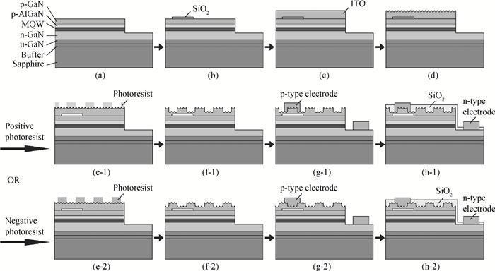
The LED chips with micro/nano-textured ITO surface were fabricated as follows and the main steps are shown in Fig. 1. Firstly, the expilayer was partially etched by ICP to expose n-type GaN layer for mesa structure. Secondly, a SiO2 layer was deposited by plasma-enhanced chemical vapor deposition (PECVD) and wet-etched as current blocking layer (CBL)[15]. Thirdly, a 230 nm-thick ITO was deposited by electron-beam evaporation as transparent conductive layer. In the evaporation process, the ITO pallets, which were composed of 90 wt% In2O3 and 10 wt% SnO2, were evaporated at a temperature of 300 ℃ and a pressure of 106 Pa, while the flow rate of O2 was 10 sccm and the deposition rate of ITO was set to be 0.05 nm/s. Subsequently, the as-deposited ITO layer was wet-etched in a solution of ITO etchant at a temperature of 50 ℃, and the etching time is 10 s. Here, no etching mask was used, and the entire ITO surface was directly in contact with the etchant, which consists of HCl, FeCl3, and deionized water. The HCl is the main component for etching, while the FeCl3 is to enhance the etching rate and stability. After the maskless wet-etching, a thin-film of positive or negative photoresist was spin-coated, and was treated by standard photolithography. In the photolithography process, a lithography mask with micro-structure was used. The micro-structure is a triangle-lattice of close-packed micro-holes, in which both the diameter and the pitch are 3 μm. This value of 3 μm is limited by the accuracy of ultraviolet exposure. Once the photoresist was developed, the triangle-lattice of close-packed micro-holes (concave pattern) or micro-pillars (convex pattern) was formed. The presentation of concave pattern or convex pattern depended on whether positive or negative photoresist had been used. Thereafter, the ITO layer was wet-etched for 7 s, and thus the micro-pattern in the photoresist was transferred onto the ITO surface. The patterned ITO was thermally annealed at 520 ℃ for 25 min while the flow rate of pure N2 gas was 20 L/min. After that, the 500 nm/500 nm/12000 nm-thick Cr/Pt/Au multiple metal films were deposited, and the metal lift-off technology was used to fabricate p-type electrodes and n-type electrodes. Then, a 70 nm-thick SiO2 layer was deposited by PECVD for passivation, and was wet-etched to expose the electrode pads for wire-bonding. Finally, the sapphire substrates were lapped down to about 100 μm, and the 2 inch-diameter wafer was diced into 10 mil × 23 mil chips by laser-scribing and breakage.

Figure  1.  Fabrication processes of LED chips with hybrid micro/nano-textured ITO surface. (a) Mesa etching, (b) CBL fabrication, (c) ITO deposition, (d) nano-texturing realized by maskless wet-eching, (e) standard photolithography for micro-texturing, (f) micro-texturing achieved by wet-etching with mask, (g) electrode fabrication, and (h) SiO2 passivation.

Following the above described fabrication process, four types of LED chips were prepared. The first type is the conventional LED chip with as-deposited flat ITO surface (i.e. flat samples). The second type is the LED chip with nano-textured ITO surface after maskless wet-etching (i.e. nano-textured samples), while the third and the fourth types are those with hybrid micro/nano-textured ITO surface (i.e. hybrid-textured samples). The micro-structures in the third and the fourth types of samples are in the form of concave and convex pattern (i.e. concave-hybrid-textured samples and convex-hybrid-textured samples), respectively.

For each of the four types of LED chips, 116 samples are fabricated. The ITO surface morphology was featured by scanning electron microscope (SEM), and the electrical and optical properties of LED chips were measured through a probe station and integrating sphere.

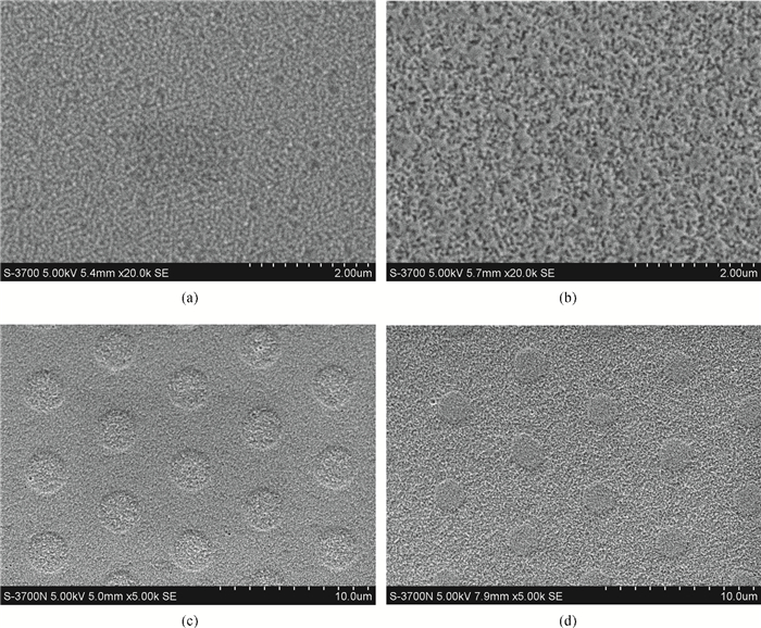
Figure 2 shows the SEM images of the ITO surface in the four types of fabricated samples. It is shown that the surface of the as-deposited ITO is not absolutely smooth. In fact, lots of grain-like particles can be found. Due to the weak binding energy at the grain boundary and the polycrystalline property[10-14], the size of the grain-like particles grew after maskless wet-etching. On the ITO surface of hybrid-textured samples, the diameter of the micro-hole and micro-pillar is about 3.2 μm and 2.4 μm, respectively. The discrepancy between the measured results and the nominal value of 3 μm determined by the lithography mask can be attributed to the isotropic wet-etching and the error of photolithography. According to the wet-etching test in advance, the etching-rate is estimated to be 7.4 nm/s, and thus the etching depth for the micro-pattern is around 51.8 nm, which is about 1/4 of the thickness of the as-deposited ITO layer.

Figure  2.  SEM images of ITO surface in (a) flat samples, (b) nano-textured samples, (c) concave-hybrid-textured samples, and (d) convex-hybrid-textured samples.

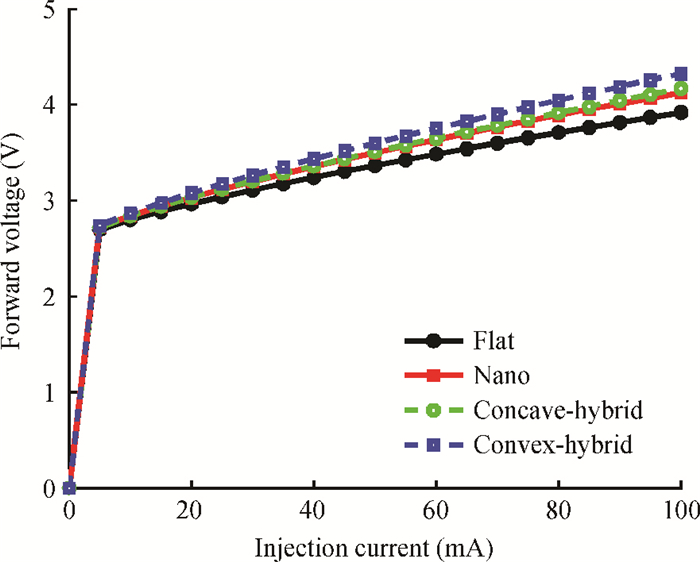
The typical values of forward voltage at different injection current of the four types of samples are shown in Fig. 3. It is shown that the textured ITO surface would induce a higher forward voltage than the flat ITO surface. This results from the reduced effective thickness of the ITO layer and thus the elevated sheet resistance. Moreover, the hybrid-textured samples have higher forward voltage than the nano-textured samples, since the volume of etched ITO in the former is more than that in the latter. For the same reason, the convex-hybrid-textured samples also have higher forward voltage than the concave-hybrid-textured samples. Under the injection current of 20 mA, the average values of forward voltages of the flat samples, nano-textured samples, concave-hybrid-textured samples, and convex-hybrid-textured samples are measured as 2.96 V, 3.02 V, 3.03 V, and 3.07 V, respectively. It suggests that the surface texturing of the ITO layer would not degrade the electrical properties of LED chips.

Figure  3.  The functional curves of forward voltage versus injection current.

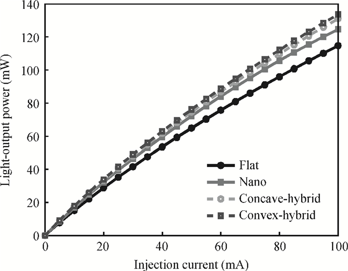
Figure 4 shows the functional curves of light-output power versus injection current for these samples. It is shown that the textured ITO surface would enhance the light-output power, compared to the flat ITO surface. This is because of the improvement of the probability of lights entering the escape cone on the textured interface between ITO and air. It is also shown that the hybrid-textured samples lead to more light extraction than the nano-textured samples, and the convex-hybrid-textured samples give the best results. At 20 mA, the average values of light-output power of the flat samples, nano-textured samples, concave-hybrid-textured samples, and convex-hybrid-textured samples are about 28.81 mW, 32.07 mW, 33.35 mW, and 33.97 mW, respectively. Compared to the flat counterparts, these three types of textured samples provide the enhancement of 11.3%, 15.8%, and 17.9%, respectively.

Figure  4.  The functional curves of light-output power versus injection current.

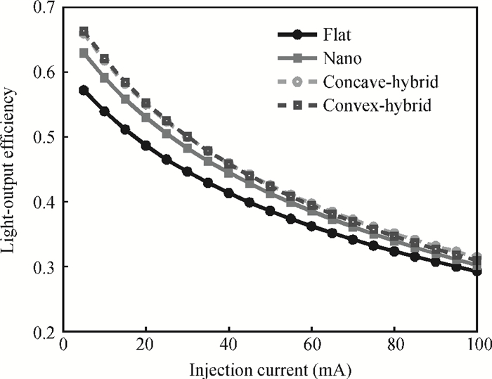
Figure 5 shows the typical values of light-output efficiency under different injection current. The light-output efficiency is defined as the light-output power divided by the electric-input power. It is shown that the light-output efficiency can be improved by ITO surface texturing, and the hybrid-textured samples have superior performance to their nano-textured counterparts. This can also be attributed to the better light-extraction efficiency. The average values of light-output efficiencies of the flat samples, nano-textured samples, concave-hybrid-textured samples, and convex-hybrid-textured samples are estimated to be 48.7%, 53.0%, 55.1%, and 55.3%, respectively, at 20 mA. Compared to the flat counterparts, these three types of textured samples provide the enhancement of 8.8%, 13.1%, and 13.5%, respectively. It is also shown that the light-output efficiency decreases significantly as the injection current increases. The convex-hybrid-textured samples have slightly higher light-output efficiency than concave-hybrid-textured samples only at small injection currents from 10 to 30 mA. On the contrary, the former has less light-output efficiency than the latter at the injection currents from 35 to 100 mA. This indicates that the concave-hybrid-textured pattern is preferred if a large injection current, such as 100 mA, is required.

Figure  5.  The functional curves of light-output efficiency versus injection current.

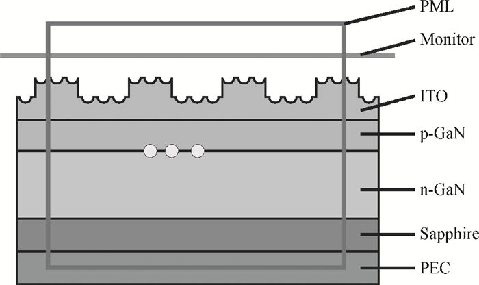
To further understand the enhancement of light-output induced by ITO texturing, the two-dimensional finite difference time domain (2D FDTD) was used for numerical simulation[16]. To reduce the computation resource, as shown in Fig. 6, the 2D model only consists of five layers, including a 2 μm-thick sapphire substrate, a 4.73 μm-thick n-type GaN, a 0.33 μm-thick p-type GaN, a 0.23 μm-thick ITO, and the perfect electrical conductor (PEC) layer below the substrate. The width of the LED chips in the simulation domain was set to be 32 μm. Since the perfect matched layer (PML) boundaries were used, the width of the chip and the thickness of the substrate can be reduced[16]. The MQW was simplified as the interface between the two types of GaN, and the electric point dipole was chosen as the source for spontaneous emission. Two orientations of dipole source along the two axes are considered, and three typical locations shown in Fig. 6 were simulated. The nano-pattern was simplified as close-packed triangles with the size of 30 nm (height) × 200 nm (width), while the concave-pattern and convex-pattern were 51.8 nm (height) × 3.2 μm (width) and 51.8 nm (height) × 2.4 μm (width), respectively, and the period of the micro-pattern is 6 μm. At the wavelength of 460 nm, the refractive indices of sapphire, GaN, and ITO are set to be 1.78, 2.45, and 2.0221, respectively. Simulation results show that the nano-pattern, concave-hybrid pattern, and convex-hybrid pattern exhibits the improvements of 14.68%, 25.93%, and 26.32%, respectively, for light-extraction efficiency. The variation trend is consistent with the experimental results, and demonstrates that the light-output can be significantly enhanced by the hybrid-textured ITO surface.

Figure  6.  2D-FDTD model for convex-hybrid-textured samples. The gray circles are the three typical locations for dipole source.

GaN-based LED chips with flat, nano-textured, concave hybrid micro/nano-textured, and convex hybrid micro/nano-textured ITO surface had been prepared in a mature product line. The nano-texturing was realized by maskless wet-etching, and the micro-texturing was achieved by standard photolithography and wet-etching. All these techniques are feasible, simple, and low cost. The results show that the textured ITO surface would induce a higher forward voltage, light-output power, and light-output efficiency than the flat ITO surface. Compared to the nano-textured samples, the forward voltage of hybrid-textured samples is slightly raised, while both the light-output power and light-output efficiency are significantly improved. Moreover, the convex-hybrid-textured samples give the highest forward voltage, and provide the best results of light-output power. Under the injection current of 20 mA, compared to the flat samples, the light-output powers of the nano-textured samples, concave-hybrid-textured samples, and convex-hybrid-textured samples are enhanced by 11.3%, 15.8%, and 17.9%, respectively. The 2D-FDTD simulation results are consistent with the experiments. However, considering the light-output efficiency, the convex-hybrid pattern shows better performance under small injection current, while the concave-hybrid pattern is preferred under large injection current. Furthermore, the electrical and optical performance can be improved further if the etching depth is optimized.

Acknowledgement: The authors would like to thank Neo-Neon LED lighting International Ltd. for its help in the experiments.


[1]
Zhmakin A I. Enhancement of light extraction from light emitting diodes. Phys Rep, 2011, 498:189 doi: 10.1016/j.physrep.2010.11.001
[2]
Pan S M, Tu R C, Fan Y M, et al. Improvement of InGaN-GaN light-emitting diodes with surface-textured indium-tin-oxide transparent ohmic contacts. IEEE Photon Tech Lett, 2003, 15(5):649 doi: 10.1109/LPT.2003.809985
[3]
Wang P, Cao B, Wei W, et al. Improved light extraction of GaN-based light-emitting diodes by ITO patterning with optimization design. Solid-State Electron, 2010, 54:283 doi: 10.1016/j.sse.2009.10.005
[4]
Tsai C F, Su Y K, Lin C L. Improvement in external quantum efficiency of InGaN-based LEDs by micro-textured surface with different geometric patterns. J Electrochem Soc, 2012, 159(2):H151 doi: 10.1149/2.055202jes
[5]
Chang S J, Shen C F, Chen W S, et al. Nitride-based light emitting diodes with indium tin oxide electrode patterned by imprint lithography. Appl Phys Lett, 2007, 91:013504 doi: 10.1063/1.2753726
[6]
Leem D S, Cho J, Sone C, et al. Light-output enhancement of GaN-based light-emitting diodes by using hole-patterned transparent indium tin oxide electrodes. J Appl Phys, 2005, 98:076107. doi: 10.1063/1.2081117
[7]
Horng R H, Yang C C, Wu J Y, et al. GaN-based light-emitting diodes with indium tin oxide texturing window layers using natural lithography. Appl Phys Lett, 2005, 86:221101 doi: 10.1063/1.1940723
[8]
He Anhe, Zhang Yong, Zhu Xuehui, et al. Improved light extraction of GaN-based light-emitting diodes with surface-textured indium tin oxide electrodes by nickel nanoparticle mask dry-etching. Chin Phys B, 2010, 19(6):068101 doi: 10.1088/1674-1056/19/6/068101
[9]
Liao C, Wu Y S. InGaN-GaN light emitting diode performance improved by roughening indium tin oxide window layer via natural lithography. Electrochem Solid State Lett, 2010, 13(1):J8 doi: 10.1149/1.3257601
[10]
Leem D S, Lee T, Seong T Y. Enhancement of the light output of GaN-based light-emitting diodes with surface-patterned ITO electrodes by maskless wet-etching. Solid-State Electron, 2007, 51:793 doi: 10.1016/j.sse.2007.02.038
[11]
Kang J H, Kim H G, Ryu J H, et al. Enhancement of light output power in InGaN/GaN LEDs with nanoroughed hemispherical indium tin oxide transparent ohmic contacts. Electrochem Solid State Lett, 2010, 13(2):D1 doi: 10.1149/1.3261741
[12]
Kang J H, Ryu J H, Kim H K, et al. Comparison of various surface textured layer in InGaN LEDs for high light extraction efficiency. Opt Express, 2011, 19(4):3637 doi: 10.1364/OE.19.003637
[13]
Kang J H, Kim H G, Kim H K, et al. Improvement of light output power in InGaN/GaN light-emitting diodes with a nanotextured GaN surface using indium tin oxide nanospheres. Jpn J Appl Phys, 2009, 48:102104 doi: 10.1143/JJAP.48.102104
[14]
Li S, Kuo D S, Liu C H, et al. Efficiency improvement of GaN-based light-emitting diodes by direct wet etching of indium-tin-oxide layer. IET Optoelectron, 2012, 6(6):303 doi: 10.1049/iet-opt.2012.0019
[15]
Huh C, Lee J M, Kim D J, et al. Improvement in light-output efficiency of InGaN/GaN multiple-quantum well light-emitting diodes by current blocking layer. J Appl Phys, 2002, 92(5):2248 doi: 10.1063/1.1497467
[16]
Pan J W, Tsai P J, Chang K D, et al. Light extraction efficiency analysis of GaN-based light-emitting diodes with nanopatterned sapphire substrates. Appl Opt, 2013, 52(7):1358 doi: 10.1364/AO.52.001358
Fig. 1.  Fabrication processes of LED chips with hybrid micro/nano-textured ITO surface. (a) Mesa etching, (b) CBL fabrication, (c) ITO deposition, (d) nano-texturing realized by maskless wet-eching, (e) standard photolithography for micro-texturing, (f) micro-texturing achieved by wet-etching with mask, (g) electrode fabrication, and (h) SiO2 passivation.

Fig. 2.  SEM images of ITO surface in (a) flat samples, (b) nano-textured samples, (c) concave-hybrid-textured samples, and (d) convex-hybrid-textured samples.

Fig. 3.  The functional curves of forward voltage versus injection current.

Fig. 4.  The functional curves of light-output power versus injection current.

Fig. 5.  The functional curves of light-output efficiency versus injection current.

Fig. 6.  2D-FDTD model for convex-hybrid-textured samples. The gray circles are the three typical locations for dipole source.

[1]
Zhmakin A I. Enhancement of light extraction from light emitting diodes. Phys Rep, 2011, 498:189 doi: 10.1016/j.physrep.2010.11.001
[2]
Pan S M, Tu R C, Fan Y M, et al. Improvement of InGaN-GaN light-emitting diodes with surface-textured indium-tin-oxide transparent ohmic contacts. IEEE Photon Tech Lett, 2003, 15(5):649 doi: 10.1109/LPT.2003.809985
[3]
Wang P, Cao B, Wei W, et al. Improved light extraction of GaN-based light-emitting diodes by ITO patterning with optimization design. Solid-State Electron, 2010, 54:283 doi: 10.1016/j.sse.2009.10.005
[4]
Tsai C F, Su Y K, Lin C L. Improvement in external quantum efficiency of InGaN-based LEDs by micro-textured surface with different geometric patterns. J Electrochem Soc, 2012, 159(2):H151 doi: 10.1149/2.055202jes
[5]
Chang S J, Shen C F, Chen W S, et al. Nitride-based light emitting diodes with indium tin oxide electrode patterned by imprint lithography. Appl Phys Lett, 2007, 91:013504 doi: 10.1063/1.2753726
[6]
Leem D S, Cho J, Sone C, et al. Light-output enhancement of GaN-based light-emitting diodes by using hole-patterned transparent indium tin oxide electrodes. J Appl Phys, 2005, 98:076107. doi: 10.1063/1.2081117
[7]
Horng R H, Yang C C, Wu J Y, et al. GaN-based light-emitting diodes with indium tin oxide texturing window layers using natural lithography. Appl Phys Lett, 2005, 86:221101 doi: 10.1063/1.1940723
[8]
He Anhe, Zhang Yong, Zhu Xuehui, et al. Improved light extraction of GaN-based light-emitting diodes with surface-textured indium tin oxide electrodes by nickel nanoparticle mask dry-etching. Chin Phys B, 2010, 19(6):068101 doi: 10.1088/1674-1056/19/6/068101
[9]
Liao C, Wu Y S. InGaN-GaN light emitting diode performance improved by roughening indium tin oxide window layer via natural lithography. Electrochem Solid State Lett, 2010, 13(1):J8 doi: 10.1149/1.3257601
[10]
Leem D S, Lee T, Seong T Y. Enhancement of the light output of GaN-based light-emitting diodes with surface-patterned ITO electrodes by maskless wet-etching. Solid-State Electron, 2007, 51:793 doi: 10.1016/j.sse.2007.02.038
[11]
Kang J H, Kim H G, Ryu J H, et al. Enhancement of light output power in InGaN/GaN LEDs with nanoroughed hemispherical indium tin oxide transparent ohmic contacts. Electrochem Solid State Lett, 2010, 13(2):D1 doi: 10.1149/1.3261741
[12]
Kang J H, Ryu J H, Kim H K, et al. Comparison of various surface textured layer in InGaN LEDs for high light extraction efficiency. Opt Express, 2011, 19(4):3637 doi: 10.1364/OE.19.003637
[13]
Kang J H, Kim H G, Kim H K, et al. Improvement of light output power in InGaN/GaN light-emitting diodes with a nanotextured GaN surface using indium tin oxide nanospheres. Jpn J Appl Phys, 2009, 48:102104 doi: 10.1143/JJAP.48.102104
[14]
Li S, Kuo D S, Liu C H, et al. Efficiency improvement of GaN-based light-emitting diodes by direct wet etching of indium-tin-oxide layer. IET Optoelectron, 2012, 6(6):303 doi: 10.1049/iet-opt.2012.0019
[15]
Huh C, Lee J M, Kim D J, et al. Improvement in light-output efficiency of InGaN/GaN multiple-quantum well light-emitting diodes by current blocking layer. J Appl Phys, 2002, 92(5):2248 doi: 10.1063/1.1497467
[16]
Pan J W, Tsai P J, Chang K D, et al. Light extraction efficiency analysis of GaN-based light-emitting diodes with nanopatterned sapphire substrates. Appl Opt, 2013, 52(7):1358 doi: 10.1364/AO.52.001358
1

Perovskite nanocrystals for light-emitting diodes

Xinyi Mei, Lixiu Zhang, Xiaoliang Zhang, Liming Ding

Journal of Semiconductors, 2022, 43(9): 090201. doi: 10.1088/1674-4926/43/9/090201

2

The strategies for preparing blue perovskite light-emitting diodes

Jianxun Lu, Zhanhua Wei

Journal of Semiconductors, 2020, 41(5): 051203. doi: 10.1088/1674-4926/41/5/051203

3

Giant efficiency and color purity enhancement in multicolor inorganic perovskite light-emitting diodes via heating-assisted vacuum deposition

Boning Han, Qingsong Shan, Fengjuan Zhang, Jizhong Song, Haibo Zeng, et al.

Journal of Semiconductors, 2020, 41(5): 052205. doi: 10.1088/1674-4926/41/5/052205

4

Light-emitting diodes based on all-inorganic copper halide perovskite with self-trapped excitons

Nian Liu, Xue Zhao, Mengling Xia, Guangda Niu, Qingxun Guo, et al.

Journal of Semiconductors, 2020, 41(5): 052204. doi: 10.1088/1674-4926/41/5/052204

5

Rational molecular passivation for high-performance perovskite light-emitting diodes

Jingbi You

Journal of Semiconductors, 2019, 40(4): 040203. doi: 10.1088/1674-4926/40/4/040203

6

Light-emitting diodes based on colloidal silicon quantum dots

Shuangyi Zhao, Xiangkai Liu, Xiaodong Pi, Deren Yang

Journal of Semiconductors, 2018, 39(6): 061008. doi: 10.1088/1674-4926/39/6/061008

7

Evaluation of light extraction efficiency for the light-emitting diodes based on the transfer matrix formalism and ray-tracing method

Pingbo An, Li Wang, Hongxi Lu, Zhiguo Yu, Lei Liu, et al.

Journal of Semiconductors, 2016, 37(6): 064015. doi: 10.1088/1674-4926/37/6/064015

8

Enhancement of blue InGaN light-emitting diodes by using AlGaN increased composition-graded barriers

Yan Lei, Zhiqiang Liu, Miao He, Xiaoyan Yi, Junxi Wang, et al.

Journal of Semiconductors, 2015, 36(5): 054006. doi: 10.1088/1674-4926/36/5/054006

9

Enhanced electroluminescence from a free-standing tensilely strained germanium nanomembrane light-emitting diode

Jingming Chen, Bin Shu, Jibao Wu, Linxi Fan, Heming Zhang, et al.

Journal of Semiconductors, 2015, 36(10): 104004. doi: 10.1088/1674-4926/36/10/104004

10

Light extraction efficiency enhancement in light-emitting diodes with indium tin oxide nano-craters

Zheng Huaiwen, Zhang Yiyun, Yang Hua, Xue Bin, Wu Kui, et al.

Journal of Semiconductors, 2012, 33(5): 054009. doi: 10.1088/1674-4926/33/5/054009

11

Improved III-nitrides based light-emitting diodes anti-electrostatic discharge capacity with an AlGaN/GaN stack insert layer

Li Zhicong, Li Panpan, Wang Bing, Li Hongjian, Liang Meng, et al.

Journal of Semiconductors, 2011, 32(11): 114007. doi: 10.1088/1674-4926/32/11/114007

12

Current–voltage characteristics of light-emitting diodes under optical and electrical excitation

Wen Jing, Wen Yumei, Li Ping, Li Lian

Journal of Semiconductors, 2011, 32(8): 084004. doi: 10.1088/1674-4926/32/8/084004

13

Degradation of light emitting diodes: a proposed methodology

Sau Koh, Willem Van Driel, G. Q. Zhang

Journal of Semiconductors, 2011, 32(1): 014004. doi: 10.1088/1674-4926/32/1/014004

14

Fluorescent SiC and its application to white light-emitting diodes

Satoshi Kamiyama, Motoaki Iwaya, Tetsuya Takeuchi, Isamu Akasaki, Mikael Syvajarvi, et al.

Journal of Semiconductors, 2011, 32(1): 013004. doi: 10.1088/1674-4926/32/1/013004

15

Properties of the ITO layer in a novel red light-emitting diode

Zhang Yonghui, Guo Weiling, Gao Wei, Li Chunwei, Ding Tianping, et al.

Journal of Semiconductors, 2010, 31(4): 043002. doi: 10.1088/1674-4926/31/4/043002

16

Room-temperature electroluminescence of p-ZnxMg1-xO:Na/n-ZnO p-n junction light emitting diode

Ye Zhizhen, Zhang Liqiang, Huang Jingyun, Zhang Yinzhu, Zhu Liping, et al.

Journal of Semiconductors, 2009, 30(8): 081001. doi: 10.1088/1674-4926/30/8/081001

17

Spectrum study of top-emitting organic light-emitting devices with micro-cavity structure

Liu Xiang, Wei Fuxiang, Liu Hui

Journal of Semiconductors, 2009, 30(4): 044007. doi: 10.1088/1674-4926/30/4/044007

18

High-Power Distributed Feedback Laser Diodes Emitting at 820nm

Fu Shenghui, Zhong Yuan, Song Guofeng, Chen Lianghui

Chinese Journal of Semiconductors , 2006, 27(6): 966-969.

19

Fabrication and Emission Properties of a n-ZnO/p-GaN Heterojunction Light-Emitting Diode

Zhou Xin, Gu Shulin, Zhu Shunming, Ye Jiandong, Liu Wei, et al.

Chinese Journal of Semiconductors , 2006, 27(2): 249-253.

20

Light Extraction Efficiency of High-Power GaN-Based Light-Emitting Diodes

Guo Jinxia, Ma Long, Yi Xiaoyan, Wang Liangchen, Wang Guohong, et al.

Chinese Journal of Semiconductors , 2005, 26(S1): 170-175.

  • Search

    Advanced Search >>

    GET CITATION

    Huamao Huang, Jinyong Hu, Hong Wang. GaN-based light-emitting diodes with hybrid micro/nano-textured indium-tin-oxide layer[J]. Journal of Semiconductors, 2014, 35(8): 084006. doi: 10.1088/1674-4926/35/8/084006
    H M Huang, J Y Hu, H Wang. GaN-based light-emitting diodes with hybrid micro/nano-textured indium-tin-oxide layer[J]. J. Semicond., 2014, 35(8): 084006. doi: 10.1088/1674-4926/35/8/084006.
    shu

    Export: BibTex EndNote

    Article Metrics

    Article views: 3246 Times PDF downloads: 26 Times Cited by: 0 Times

    History

    Received: 19 February 2014 Revised: 04 April 2014 Online: Published: 01 August 2014

    Catalog

      Email This Article

      User name:
      Email:*请输入正确邮箱
      Code:*验证码错误
      Huamao Huang, Jinyong Hu, Hong Wang. GaN-based light-emitting diodes with hybrid micro/nano-textured indium-tin-oxide layer[J]. Journal of Semiconductors, 2014, 35(8): 084006. doi: 10.1088/1674-4926/35/8/084006 ****H M Huang, J Y Hu, H Wang. GaN-based light-emitting diodes with hybrid micro/nano-textured indium-tin-oxide layer[J]. J. Semicond., 2014, 35(8): 084006. doi: 10.1088/1674-4926/35/8/084006.
      Citation:
      Huamao Huang, Jinyong Hu, Hong Wang. GaN-based light-emitting diodes with hybrid micro/nano-textured indium-tin-oxide layer[J]. Journal of Semiconductors, 2014, 35(8): 084006. doi: 10.1088/1674-4926/35/8/084006 ****
      H M Huang, J Y Hu, H Wang. GaN-based light-emitting diodes with hybrid micro/nano-textured indium-tin-oxide layer[J]. J. Semicond., 2014, 35(8): 084006. doi: 10.1088/1674-4926/35/8/084006.

      GaN-based light-emitting diodes with hybrid micro/nano-textured indium-tin-oxide layer

      DOI: 10.1088/1674-4926/35/8/084006
      Funds:

      the Fundamental Research Funds for the Central Universities 2013ZM093

      the Fundamental Research Funds for the Central Universities 2013ZP0017

      the National High Technology Research and Development Program of China 2014AA032609

      the Strategic Emerging Industry Special Funds of Guangdong Province 2010A081002009

      the Strategic Emerging Industry Special Funds of Guangdong Province 2011A081301004

      Project supported by the National High Technology Research and Development Program of China (No. 2014AA032609), the Strategic Emerging Industry Special Funds of Guangdong Province (Nos. 2010A081002009, 2011A081301004, 2012A080302003), and the Fundamental Research Funds for the Central Universities (Nos. 2013ZM093, 2013ZP0017)

      the Strategic Emerging Industry Special Funds of Guangdong Province 2012A080302003

      More Information
      • Corresponding author: Wang Hong, Email:phhwang@scut.edu.cn
      • Received Date: 2014-02-19
      • Revised Date: 2014-04-04
      • Published Date: 2014-08-01

      Catalog

        /

        DownLoad:  Full-Size Img  PowerPoint
        Return
        Return