


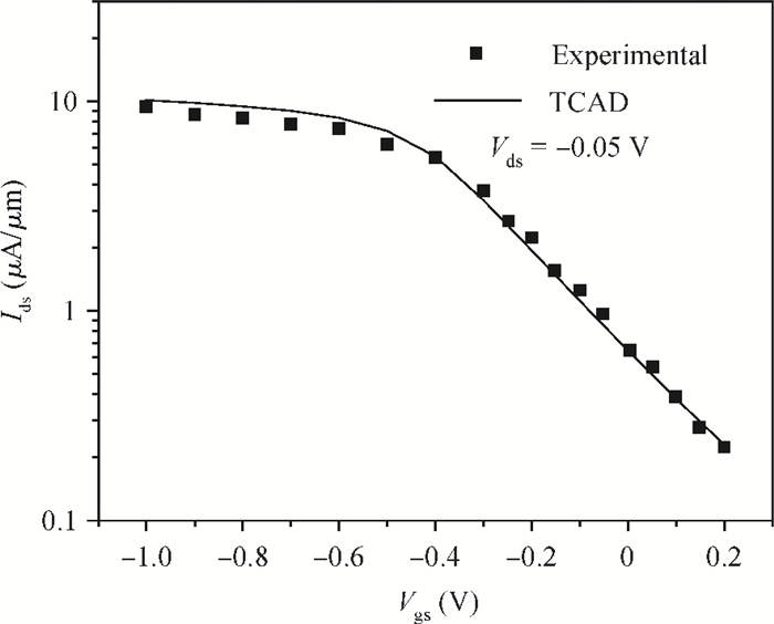
Fig. 1.
Comparison of simulated and experimental transfer characteristics of GeOI pMOSFET for Vds D 0:05 V
SEMICONDUCTOR DEVICES
Yurong Bai, Jingping Xu, Lu Liu and Minmin Fan
Corresponding author: Xu Jingping, Email:jpxu@mail.hust.edu.cn
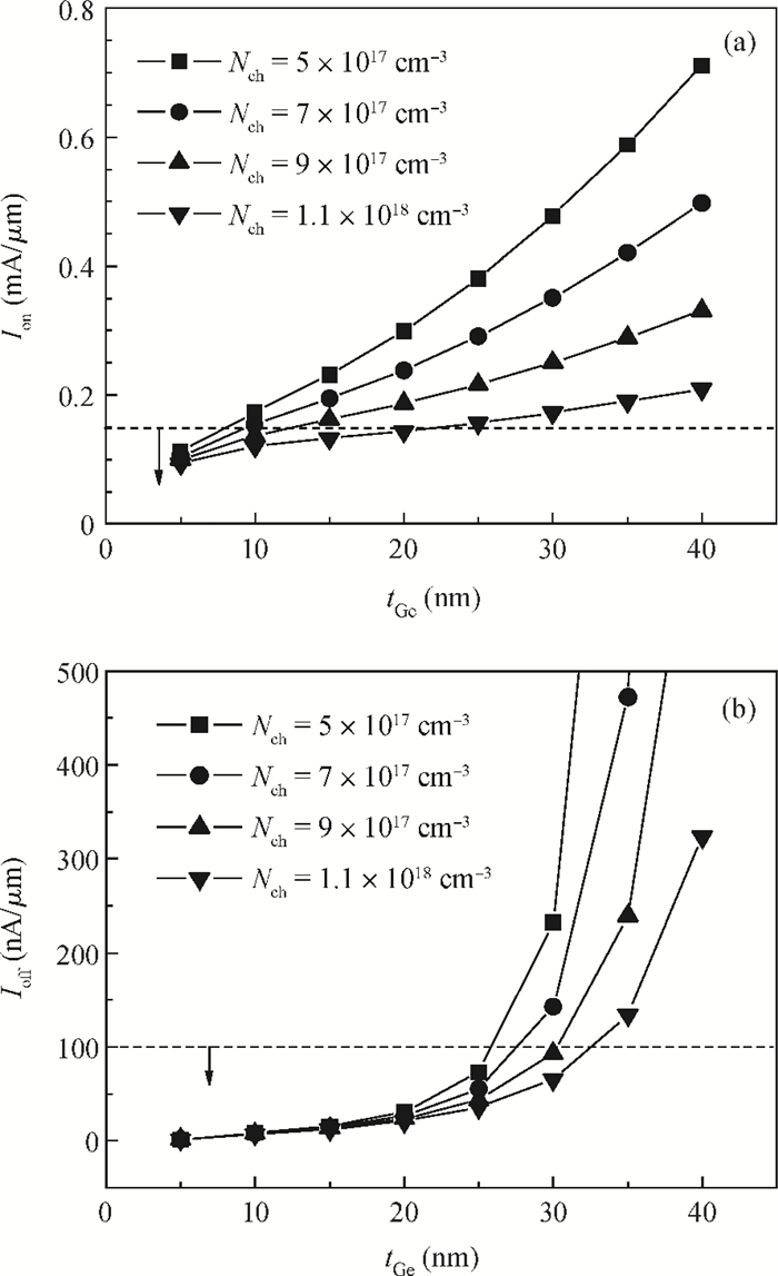
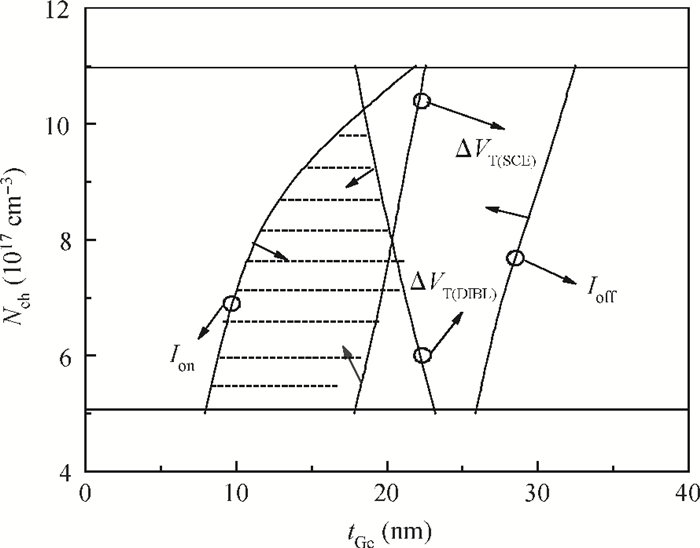
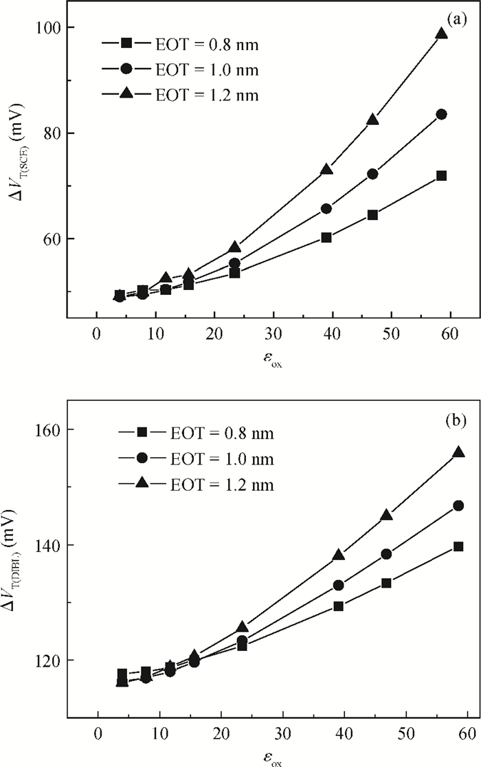
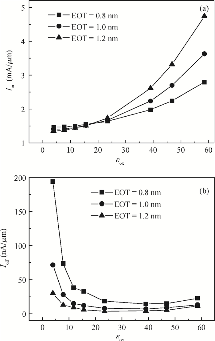
Abstract: The influences of the main structure and physical parameters of the dual-gate GeOI MOSFET on the device performance are investigated by using a TCAD 2D device simulator. A reasonable value range of germanium (Ge) channel thickness, doping concentration, gate oxide thickness and permittivity is determined by analyzing the on-state current, off-state current, short channel effect (SCE) and drain-induced barrier lowering (DIBL) effect of the GeOI MOSFET. When the channel thickness and its doping concentration are 10-18 nm and (5-9)×1017 cm-3, and the equivalent oxide thickness and permittivity of the gate dielectric are 0.8-1 nm and 15-30, respectively, excellent device performances of the small-scaled GeOI MOSFET can be achieved:on-state current of larger than 1475 μA/μm, off-state current of smaller than 0.1 μA/μm, SCE-induced threshold-voltage drift of lower than 60 mV and DIBL-induced threshold-voltage drift of lower than 140 mV.
Keywords: GeOI MOSFET, high-k gate dielectric, short-channel effect, drain-induced barrier lowering effect
| [1] |
Paussa A, Conzatti F, Breda D, et al. Pseudospectral methods for the efficient simulation of quantization effects in nanoscale MOS transistors. IEEE Trans Electron Devices, 2012, 57(12):104002 http://ieeexplore.ieee.org/document/5610722/
|
| [2] |
Hu Aibin, Xu Qiuxia. Effects of silicon nitride diffusion barrier on germanium MOS capacitors with HfON gate dielectrics. Journal of Semiconductors, 2009, 30(10):59 http://www.jos.ac.cn/bdtxbcn/ch/reader/view_abstract.aspx?file_no=09031501&flag=1
|
| [3] |
Hu V P H, Fan M L, Su P, et al. Analysis of power-performance for ultra-thin-body GeOI logic circuits. Low Power Electronics and Design International Symposium, Fukuoka, 2011:115 http://ieeexplore.ieee.org/Xplore/home.jsp
|
| [4] |
Van Den Daelea W, Augendre E, Le Royer C, et al. Low-temperature characterization and modeling of advanced GeOI pMOSFETs:mobility mechanisms and origin of the parasitic conduction. Solid-State Electron, 2010, 54(2):205 doi: 10.1016/j.sse.2009.12.020
|
| [5] |
Romanjek K, Hutin L, Le Royer C, et al. High performance 70 nm gate length germanium-on-insulator pMOSFET with high-k/metal gate. Microelectron Eng, 2009, 53(7):723 http://ieeexplore.ieee.org/document/4681702/
|
| [6] |
Romanjek K, Augendre E, Van Den Daele W, et al. Improved GeOI substrates for pMOSFET off-state leakage control. Microelectron Eng, 2009, 86(7-9):1585 doi: 10.1016/j.mee.2009.03.069
|
| [7] |
Yu C H, Wu Y S, Hu V P H, et al. Impact of quantum confinement on backgate-bias modulated threshold-voltage and subthreshold characteristics for ultra-thin-body GeOI MOSFETs. IEEE Trans Electron Devices, 2012, 59(7):1851 doi: 10.1109/TED.2012.2194499
|
| [8] |
Yu C H, Wu Y S, Hu V P H, et al. Impact of quantum confinement on subthreshold swing and electrostatic integrity of ultra-thin-body GeOI and InGaAs-OI n-MOSFETs. IEEE Trans Nanotechnology, 2012, 11(2):287 doi: 10.1109/TNANO.2011.2169084
|
| [9] |
Liu K M, Hsieh Y Y. Investigation of the dimension effects of 30-nm below multiple-gate SOI MOSFETs by TCAD simulation. IEEE 4th INEC, Tao-Yuan, 2011:1 http://ieeexplore.ieee.org/document/5991679/?arnumber=5991679&contentType=Conference%20Publications
|
| [10] |
Yuki T, Yasuhisa O. Empirical quantitative modeling of threshold voltage of sub-50-nm double-gate silicon-on-insulator metal-oxide-semiconductor field-effect transistor. Jpn J Appl Phys, 2006, 45(4B):3074 doi: 10.1143/JJAP.45.3074
|
| [11] |
Louis H, Cyrille L R, Jean F D, et al. GeOI pMOSFETs scaled down to 30-nm gate length with record off-state current. IEEE Electron Device Lett, 2010, 31(3):234 doi: 10.1109/LED.2009.2038289
|
| [12] |
Wu Y S, Hsieh H Y, Hu V P H, et al. Impact of quantum confinement on short-channel effects for ultrathin-body germanium-on-insulator MOSFETs. IEEE Electron Device Lett, 2011, 32(1):18 doi: 10.1109/LED.2010.2089425
|
| [13] |
Hutin L, Royer C L, Damlencourt J F, et al. GeOI pMOSFETs scaled down to 30-nm gate length with record off-state current. IEEE Electron Device Lett, 2010, 31(3):324 http://ieeexplore.ieee.org/document/5398976/
|
| [14] |
Technology Roadmap for Semiconductors (ITRS) 2012. http://www.itrs.net
|
| [15] |
Wu Meile, Jin Xiaoshi, Chuai Rongyan, et al. Simulation study on short channel double-gate junctionless field-effect transistors. Journal of Semiconductors, 2013, 34(12):124001 doi: 10.1088/1674-4926/34/12/124001
|
| [16] |
Razavi P, Orouji A A. Dual material gate oxide stack symmetric double gate MOSFET:improving short channel effects of nanoscale double gate MOSFET. International Biennial Baltic Electronics Conference, Tallinn, 2008:83 http://ieeexplore.ieee.org/document/4657483/?reload=true&arnumber=4657483&punumber%3D4651691
|
| [17] |
Hu V P H, Fan M L, Su P, et al. Band-to-band-tunneling leakage suppression for ultra-thin-body GeOI MOSFETs using transistor stacking. IEEE Electron Device Lett, 2012, 33(2):197 doi: 10.1109/LED.2011.2177955
|
| [18] |
Liu H X, Ma F, Fan J B, et al. Off-state leakage current of nano-scaled MOSFETs with high-k gate dielectric. IEEE 11th International Conference Solid-State and Integrated Circuit Technology, Xi'an, 2012:1 http://ieeexplore.ieee.org/document/4657483/?reload=true&arnumber=4657483&punumber%3D4651691
|
| [19] |
Chen H F, Guo L X. Influence of gate voltage on gate-induced drain leakage current in ultra-thin gate oxide and ultra-short channel LDD nMOSFET's. Acta Phys Sin, 2012, 61(2):2 http://www.sciencedirect.com/science/article/pii/S0026271499002048
|


Article views: 3173 Times PDF downloads: 15 Times Cited by: 0 Times
Received: 05 January 2014 Revised: 26 February 2014 Online: Published: 01 September 2014
| Citation: |
Yurong Bai, Jingping Xu, Lu Liu, Minmin Fan. Simulation of electrical characteristics and structural optimization for small-scaled dual-gate GeOI MOSFET with high-k gate dielectric[J]. Journal of Semiconductors, 2014, 35(9): 094002. doi: 10.1088/1674-4926/35/9/094002
****
Y R Bai, J P Xu, L Liu, M M Fan. Simulation of electrical characteristics and structural optimization for small-scaled dual-gate GeOI MOSFET with high-k gate dielectric[J]. J. Semicond., 2014, 35(9): 094002. doi: 10.1088/1674-4926/35/9/094002.

|
| [1] |
Paussa A, Conzatti F, Breda D, et al. Pseudospectral methods for the efficient simulation of quantization effects in nanoscale MOS transistors. IEEE Trans Electron Devices, 2012, 57(12):104002 http://ieeexplore.ieee.org/document/5610722/
|
| [2] |
Hu Aibin, Xu Qiuxia. Effects of silicon nitride diffusion barrier on germanium MOS capacitors with HfON gate dielectrics. Journal of Semiconductors, 2009, 30(10):59 http://www.jos.ac.cn/bdtxbcn/ch/reader/view_abstract.aspx?file_no=09031501&flag=1
|
| [3] |
Hu V P H, Fan M L, Su P, et al. Analysis of power-performance for ultra-thin-body GeOI logic circuits. Low Power Electronics and Design International Symposium, Fukuoka, 2011:115 http://ieeexplore.ieee.org/Xplore/home.jsp
|
| [4] |
Van Den Daelea W, Augendre E, Le Royer C, et al. Low-temperature characterization and modeling of advanced GeOI pMOSFETs:mobility mechanisms and origin of the parasitic conduction. Solid-State Electron, 2010, 54(2):205 doi: 10.1016/j.sse.2009.12.020
|
| [5] |
Romanjek K, Hutin L, Le Royer C, et al. High performance 70 nm gate length germanium-on-insulator pMOSFET with high-k/metal gate. Microelectron Eng, 2009, 53(7):723 http://ieeexplore.ieee.org/document/4681702/
|
| [6] |
Romanjek K, Augendre E, Van Den Daele W, et al. Improved GeOI substrates for pMOSFET off-state leakage control. Microelectron Eng, 2009, 86(7-9):1585 doi: 10.1016/j.mee.2009.03.069
|
| [7] |
Yu C H, Wu Y S, Hu V P H, et al. Impact of quantum confinement on backgate-bias modulated threshold-voltage and subthreshold characteristics for ultra-thin-body GeOI MOSFETs. IEEE Trans Electron Devices, 2012, 59(7):1851 doi: 10.1109/TED.2012.2194499
|
| [8] |
Yu C H, Wu Y S, Hu V P H, et al. Impact of quantum confinement on subthreshold swing and electrostatic integrity of ultra-thin-body GeOI and InGaAs-OI n-MOSFETs. IEEE Trans Nanotechnology, 2012, 11(2):287 doi: 10.1109/TNANO.2011.2169084
|
| [9] |
Liu K M, Hsieh Y Y. Investigation of the dimension effects of 30-nm below multiple-gate SOI MOSFETs by TCAD simulation. IEEE 4th INEC, Tao-Yuan, 2011:1 http://ieeexplore.ieee.org/document/5991679/?arnumber=5991679&contentType=Conference%20Publications
|
| [10] |
Yuki T, Yasuhisa O. Empirical quantitative modeling of threshold voltage of sub-50-nm double-gate silicon-on-insulator metal-oxide-semiconductor field-effect transistor. Jpn J Appl Phys, 2006, 45(4B):3074 doi: 10.1143/JJAP.45.3074
|
| [11] |
Louis H, Cyrille L R, Jean F D, et al. GeOI pMOSFETs scaled down to 30-nm gate length with record off-state current. IEEE Electron Device Lett, 2010, 31(3):234 doi: 10.1109/LED.2009.2038289
|
| [12] |
Wu Y S, Hsieh H Y, Hu V P H, et al. Impact of quantum confinement on short-channel effects for ultrathin-body germanium-on-insulator MOSFETs. IEEE Electron Device Lett, 2011, 32(1):18 doi: 10.1109/LED.2010.2089425
|
| [13] |
Hutin L, Royer C L, Damlencourt J F, et al. GeOI pMOSFETs scaled down to 30-nm gate length with record off-state current. IEEE Electron Device Lett, 2010, 31(3):324 http://ieeexplore.ieee.org/document/5398976/
|
| [14] |
Technology Roadmap for Semiconductors (ITRS) 2012. http://www.itrs.net
|
| [15] |
Wu Meile, Jin Xiaoshi, Chuai Rongyan, et al. Simulation study on short channel double-gate junctionless field-effect transistors. Journal of Semiconductors, 2013, 34(12):124001 doi: 10.1088/1674-4926/34/12/124001
|
| [16] |
Razavi P, Orouji A A. Dual material gate oxide stack symmetric double gate MOSFET:improving short channel effects of nanoscale double gate MOSFET. International Biennial Baltic Electronics Conference, Tallinn, 2008:83 http://ieeexplore.ieee.org/document/4657483/?reload=true&arnumber=4657483&punumber%3D4651691
|
| [17] |
Hu V P H, Fan M L, Su P, et al. Band-to-band-tunneling leakage suppression for ultra-thin-body GeOI MOSFETs using transistor stacking. IEEE Electron Device Lett, 2012, 33(2):197 doi: 10.1109/LED.2011.2177955
|
| [18] |
Liu H X, Ma F, Fan J B, et al. Off-state leakage current of nano-scaled MOSFETs with high-k gate dielectric. IEEE 11th International Conference Solid-State and Integrated Circuit Technology, Xi'an, 2012:1 http://ieeexplore.ieee.org/document/4657483/?reload=true&arnumber=4657483&punumber%3D4651691
|
| [19] |
Chen H F, Guo L X. Influence of gate voltage on gate-induced drain leakage current in ultra-thin gate oxide and ultra-short channel LDD nMOSFET's. Acta Phys Sin, 2012, 61(2):2 http://www.sciencedirect.com/science/article/pii/S0026271499002048
|

 WeChat ID
Journal of Semiconductors © 2017 All Rights Reserved 京ICP备05085259号-2

 DownLoad:

