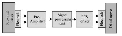
1. School of Electronics and Information, Nantong University, Nantong 226019, ChinaSchool of Electronics and Information, Nantong University, Nantong 226019, China
2. Institute of RF- & OE-ICs, Southeast University, Nanjing 210096, ChinaInstitute of RF- & OE-ICs, Southeast University, Nanjing 210096, China
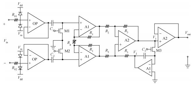
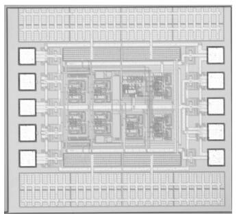
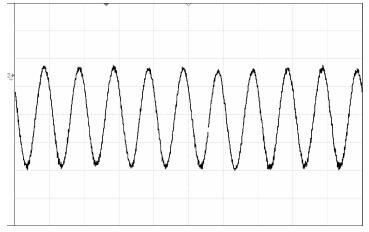
Abstract: Nerve tracts interruption is one of the major reasons for dysfunction after spiral cord injury. The microelectronic neural bridge is a method to restore function of interrupted neural pathways, by making use of microelectronic chips to bypass the injured nerve tracts. A low-power fully integrated microelectronic neural bridge chip is designed, using CSMC 0.5-μm CMOS technology. The structure and the key points in the circuit design will be introduced in detail. In order to meet the requirement for implantation, the circuit was modified to avoid the use of off-chip components, and fully monolithic integration is achieved. The operating voltage of the circuit is ±2.5 V, and the chip area is 1.21×1.18 mm2. According to the characteristic of neural signal, the time-domain method is used in testing. The pass bandwidth of the microelectronic neural bridge system covers the whole frequency range of the neural signal, power consumption is 4.33 mW, and the gain is adjustable. The design goals are achieved.
As we know, the functions of an interrupted spinal cord can hardly be repaired by the biological methods. With the development of microelectronics, more and more microelectronic devices have been used in biomedical engineering[1, 2]. Electronic devices used as functional electrical stimulation (FES) have already been used in many aspects of functional rehabilitation such as stepping[3], hearing[4], and sensory[5].
In 2004, Wang et al. put forward an idea of a MENB (microelectronic neural bridge), which could used to restore the function of an interrupted spinal cord with a microelectronic chip[6]. Different from other functional electrical stimulation devices, the signal sources of MENB were from the organism itself rather than an artificial signal. When the spinal cord is interrupted, two microelectronic arrays (MEAs) are interfaced to the upper and lower stump of the injured spinal cord. Some of the contacts in each MEA are used for signal detecting and the rest for FES. The motion controlling signals from the brain are detected from the upper (proximal) stump of the injured spinal cord with MEA and transported to the lower (distal) stump of the injured spinal cord with a microelectronic module, and then the motor functions can be rebuilt. On the other hand, sensory nerve signals can be detected from the lower (distal) stump of the injured spinal cord and transported to the upper (proximal) stump of the injured spinal cord with another microelectronic module, then the sensory functions can be rebuilt. So the microelectronic module acts as a bridge between interrupted spinal cord stumps and is called a microelectronic neural bridge (MENB).
In the last eight years, our research group has developed three hybrid and monolithic integrated electronic systems called MENB for the channel bridge and signal regeneration of injured spinal cords.
The first set of the MENB is a PCB (printed circuit board) module system based on commercial chips[7]. The first set of the system has been successfully used in animal experiments with model of rats and toads[8]. The experimental results show that the sciatic nerve signals derived from one toad or rat have been regenerated for another toad or rat. The MENB technique has been demonstrated and proved feasible and the original idea through the first set of the MENB. However, in view of the system, it is based on the composition of the PCB module and is large in size and power consumption. There is a considerable distance with implantable devices. In order to reduce the volume and power consumption, the second set of MENB has been designed. The core of the system chip including three low-power amplifiers, two rail-to-rail amplifiers and several resistors was designed in 0.5-μm DPDM CMOS technology based at the CSMC company (Wuxi) and encapsulated in DIP14, which then formed the second set of MENB together with the chip capacitors, chip resistors and two followers through the PCB. The second set of MENB has been used in animal experiments. The result of correlation function analysis shows that the regenerated signal is correlated with the source sciatic signal significantly[9] and the MENB works well and can be used in nerve signal regeneration. The second set is smaller and the power dissipation is lower than the first set, but owing to the part of elements of the second set of MENB, such as the two followers, several chip capacitors and chip resistors that are on the PCB, its volume is not small enough and its power dissipation is not low enough to be used as an implantable device yet. So we pushed our work forward and designed the third set of MENB on improving the integration and lower power dissipation. For these reasons, a fully integrated low-power microelectronics neural bridge system is designed in this paper.
2.
The system architecture of fully integrated low-power MENB
Based on the literature and our previous experiment results, the neural signal amplitude ranges from several μV to several hundred μV with the main energy spectrum in 0.1-7 kHz[10]. According to these characteristics of neural signal, we designed a fully integrated low-power MENB. The MENB system block diagram is shown in Fig. 1. Weak neural signals detected by the detecting electrode are amplified by the pre-amplifier and then filtered and identified by the neural signal processor. The extracted nerve signals are used to control the FES generator. Finally, the FES signal is applied to the stimulating electrode, which will send signals to the damaged nerve distal neurons. The circuit structure of the MENB is shown in Fig. 2.
R01 and R02, two 1-kΩ resistors, are used in the input terminal of the MENB system for ESD protection. ESD protection has the following four functions. Firstly, electrostatic breakdown and floating input are prevented. Secondly, two opposite diodes share the voltage between Vdd and Vss, therefore, the electrostatic potential of the two input terminals are both zero. Thirdly, a low-pass filter is obtained, because of the joint action of the 1-kΩ resistors and the parasitic capacitor in the input terminal. Finally, the 1-kΩ resistors have a small effect on the buffer stage, since the input resistor of the buffer stage and the internal resistance of the signal source are quite large.
The input stage following the ESD protection circuit is an operational amplifier working as a follower. As a result, the input resistance of the amplifier circuit is increased, and this stage together with C1, C2, and the source drain equivalent resistor of M1 and M2, forms an input buffer stage. One of the reasons why we use this structure is that the neural signal source itself is a weak signal source. The voltage from the detection electrodes is in the range of microvolts. The signal source has an unstable high internal resistance, when electrodes are used to detect signals. The impedance of the signal source is not only dependent on individuals and physiological states, but also on the position of the electrodes and the physical states of the electrodes themselves. Theoretically, source impedance is a function of the frequency of the signal, the impedance of the electrodes is also dependant on the frequency, and both of them decrease with increased frequency. If the input impedance is not high enough compared with the source impedance, the low frequency component of the signal will decrease, as a result, low frequency distortion happens. The impedance of the electrodes also changes with the current density within them. Also, the internal resistance of the neural signal source connecting to the input terminal of the amplifier is up to 100 kΩ, the input impedance of the amplifier should be at least 1 MΩ, because the input impedance of the amplifier should be 100 times as large as the internal impedance of the signal source, otherwise, there will be distortions and errors. The other reason is that all kinds of physiological activities within the organism will produce huge noise and interference, and the noise performance of the pre-stage decides the one of the whole system. Hence, reducing the noise of the pre-stage is one of the main tasks in amplifier design. Differential amplifier is adapted in MENB, in order to increase the common mode rejection ratio (CMRR). As a result, common mode noise is reduced effectively. However, the actual common mode rejection capability of the neural signal detecting circuit is affected by the electrode system in front of the amplifier. Normally, the equivalent source impedances detected by two electrodes are not exactly equal, when electrodes are used to detect neural signals, and this unequal outcome is inevitable. This unequal aspect leads to the transition of common mode signals to differential mode ones, as a result, the common mode interference goes to the output without being rejected effectively. Therefore, high CMRR of the amplifier itself is not so helpful for the whole system. However, the increased input impedance of the amplifier can help reducing the transition rate of common mode signals to differential mode ones. Hence, increasing the input impedance of the amplifier is a must. Because of all these reasons, two followers are used in the input terminal which connects to two detecting electrodes, in order to increase the input impedance of the amplifier. Then, the anti-jamming capability is improved and the signals can be detected effectively.
2.2
The unit for neural signal process
A neural signal is an unstable physiological signal. However, when the neural signal represents physiological changes and is detected by electrodes, they become electrical signals and can be further processed. There are a lot of methods, techniques and circuits in the field. As for active regeneration of a central neural signal, it can be realized by using an AD converter, digital signal process techniques and a DA converter. In order to simplify the circuit and to reduce power consumption, signals are amplified and then go through a filter, which is a traditional method.
In order to compress common mode noise, and to prevent it from being introduced into the microelectronic nerve bridge, two low-noise low-power operational amplifiers A1 and A2 are used to form a three operational amplifier structure. Another operational amplifier A1 between V1 and V2, together with the equivalent drain-source resistor of M3 and the capacitor C3 forms a Miller integrator, which works as a negative voltage feedback loop. As a result, the DC and low frequency voltage components as well as AC-coupling are suppressed.
A filter is a frequency selective circuit, which means signals of certain frequencies can go through it with a fixed gain, but other ones will be attenuated greatly. Therefore, the filter is a key component used to separate a signal from interference and noise. An analogue filter is used in dynamic signal process, such as the neural signal process, since it can filter out the noise and realize the function of anti-aliasing.
The low-frequency limit of the MENB system is
f−3dB=12πRds3C3,
(1)
where Rds3 is the equivalent drain-source resistor of M3.
The gain of the MENB system is:
AV=−R3R2(1+2R1Rg),
(2)
where Rg is an adjustable resistor outside the chip, and the gain of the microelectronic nerve bridge is then adjustable.
3.
Technology selection for MENB
The CSMC Company (Wuxi) is a foundry in China, which has 0.6/0.5-μm CMOS technology and 4-μm BiCMOS technology. For the IC design in this paper, CSMC 0.5-μm DPDM CMOS technology is adapted, based on the following considerations:
(1) CMOS technology is the most popular technology, and the cost is lower than other technologies. Compared with 0.25-μm, 0.18-μm CMOS technology, by using CSMC 0.5-μm CMOS technology, the cost per unit area is much lower. Therefore, the cost for the following research and development as well as the production could be greatly reduced.
(2) A neural signal is a low frequency signal, and 0.5-μm CMOS technology could meet the frequency requirements. If we use 0.25-μm or 0.18-μm CMOS technology, the cost will be much higher without many benefits.
(3) It is a technology owned by a local company, and the chips can be designed and produced in China. The company in Wuxi has independent intellectual property rights, so we can get technology support easily, and the development period could be reduced.
4.
Electrical measurement results of a fully integrated MENB system
Figure 3 is the chip photo of the MENB chip, using CSMC 2P3M 0.5-μm standard CMOS technology, and the chip area is 1.21 × 1.18 mm2. An Agilent 33220A arbitrary waveform generator and an Agilent 54624 oscilloscope are used in the measurement of the neural signal active regeneration micro-module. One of the differential inputs is connected to the ground, and the signal end time domain measurement is adapted. The input signal is a 5-mVpp, 2-kHz sinusoid wave, and Figure 4 is the corresponding output waveform of the fully integrated MENB system. Figure 5 is the amplitude-frequency characteristic curve of the chip with sinusoid input signal and an external resistor Rg= 10 kΩ. The measured power consumption is 4.33 mW. The equivalent input noise voltage is 23 nV/rt Hz @ 1 kHz.
Figure
3.
Chip photo of the fully integrated MENB system.
The microelectronic neural bridge is a key component for neural signal regeneration and function rebuilding. In this paper, we study and design a low-power fully integrated microelectronic neural bridge circuit. The measurement results of the amplitude-frequency characteristic of the system show that the transmission band in which the signal can be amplified covers the whole frequency range of the neural signal, and the gain is large enough. Therefore, this system can be used in neural signal detection and FES. The power consumption is only 4.3 mW, which is reduced effectively compared with 40 mW of the previous generations[7, 9], which makes it more possible to implant the microelectronic neural bridge into the human body.
References
[1]
Serruya M D, Kahana M J. Techniques and devices to restore cognition. Behavioral Brain Research, 2008, 192(2):149 doi: 10.1016/j.bbr.2008.04.007
[2]
Li H, Zhao W, Zhang Y. Micropower fully integrated CMOS readout interface for neural recording application. Microelectron Reliab, 2010, 50(2):273 doi: 10.1016/j.microrel.2009.09.013
[3]
Chao T, Askari S, de Leon R, et al. A system to integrate electrical stimulation with robotically controlled treadmill training to rehabilitate stepping after spinal cord injury. IEEE Trans Neural Syst Rehabil Eng, 2012, 20(5):730 doi: 10.1109/TNSRE.2012.2202292
[4]
Zhang J, Zhang X. Electrical stimulation of the dorsal cochlear nucleus induces hearing in rats. Brain Research, 2010, 1311:37 doi: 10.1016/j.brainres.2009.11.032
[5]
Tanriverdi T, Al-Jehani H, Poulin N, et al. Functional results of electrical cortical stimulation of the lower sensory strip. Journal of Clinical Neuroscience, 2009, 16(9):1188 doi: 10.1016/j.jocn.2008.11.010
[6]
Wang Z G, Lü X Y, Gu X S. Study of detecting, processing and rebuilding of central neural signals by using microelectronics. J Commun Comput, 2004:77
[7]
Huang Z, Wang Z, Lu X, et al. Design and experiment of a neural signal detection using a FES driving system. Annual International Conference of the IEEE Engineering in Medicine and Biology Society (EMBC), 2010:1523 http://yadda.icm.edu.pl/yadda/element/bwmeta1.element.ieee-000005626834
[8]
Shen X, Wang Z, Lu X, et al. Experimental research on rebuilding the motive functions of a controlled spinal toad using MENB. High Technol Lett, 2011, 21(5):530
[9]
Shen Xiaoyan, Wang Zhigong, Lu Xiaoying, et al. Microelectronic neural bridge for signal regeneration and function rebuilding over two separate nerves. Journal of Semiconductors, 2011, 32(6):065011 doi: 10.1088/1674-4926/32/6/065011
[10]
Wang Z G, Lü X Y, Gu X S. Research of central nerve signal recording, processing and regeneration with microelectronics devices. 14th Conference on Neural Networks of China, Anhui, 2004
Chinese Journal of Semiconductors , 2002, 23(9): 988-995.
Search
GET CITATION
Xiaoyan Shen, Zhigong Wang. Fully integrated circuit chip of microelectronic neural bridge[J]. Journal of Semiconductors, 2014, 35(9): 095011. doi: 10.1088/1674-4926/35/9/095011
X Y Shen, Z G Wang. Fully integrated circuit chip of microelectronic neural bridge[J]. J. Semicond., 2014, 35(9): 095011. doi: 10.1088/1674-4926/35/9/095011.
Export: BibTexEndNote
Share:
Article Metrics
Article views: 2463 TimesPDF downloads: 12 TimesCited by: 0 Times
History
Received: 20 January 2014Revised: 21 March 2014Online:Published: 01 September 2014
X Y Shen, Z G Wang. Fully integrated circuit chip of microelectronic neural bridge[J]. J. Semicond., 2014, 35(9): 095011. doi: 10.1088/1674-4926/35/9/095011.
Xiaoyan Shen, Zhigong Wang. Fully integrated circuit chip of microelectronic neural bridge[J]. Journal of Semiconductors, 2014, 35(9): 095011. doi: 10.1088/1674-4926/35/9/095011 ****X Y Shen, Z G Wang. Fully integrated circuit chip of microelectronic neural bridge[J]. J. Semicond., 2014, 35(9): 095011. doi: 10.1088/1674-4926/35/9/095011.
X Y Shen, Z G Wang. Fully integrated circuit chip of microelectronic neural bridge[J]. J. Semicond., 2014, 35(9): 095011. doi: 10.1088/1674-4926/35/9/095011.
School of Electronics and Information, Nantong University, Nantong 226019, China
2.
Institute of RF- & OE-ICs, Southeast University, Nanjing 210096, China
Funds:
Project supported by the National Natural Science Foundation of China (Nos. 81371663, 61204018) and the Natural Science Foundation of Nantong University (No. 13B06)
the Natural Science Foundation of Nantong University13B06
the National Natural Science Foundation of China61204018
the National Natural Science Foundation of China81371663
Nerve tracts interruption is one of the major reasons for dysfunction after spiral cord injury. The microelectronic neural bridge is a method to restore function of interrupted neural pathways, by making use of microelectronic chips to bypass the injured nerve tracts. A low-power fully integrated microelectronic neural bridge chip is designed, using CSMC 0.5-μm CMOS technology. The structure and the key points in the circuit design will be introduced in detail. In order to meet the requirement for implantation, the circuit was modified to avoid the use of off-chip components, and fully monolithic integration is achieved. The operating voltage of the circuit is ±2.5 V, and the chip area is 1.21×1.18 mm2. According to the characteristic of neural signal, the time-domain method is used in testing. The pass bandwidth of the microelectronic neural bridge system covers the whole frequency range of the neural signal, power consumption is 4.33 mW, and the gain is adjustable. The design goals are achieved.
As we know, the functions of an interrupted spinal cord can hardly be repaired by the biological methods. With the development of microelectronics, more and more microelectronic devices have been used in biomedical engineering[1, 2]. Electronic devices used as functional electrical stimulation (FES) have already been used in many aspects of functional rehabilitation such as stepping[3], hearing[4], and sensory[5].
In 2004, Wang et al. put forward an idea of a MENB (microelectronic neural bridge), which could used to restore the function of an interrupted spinal cord with a microelectronic chip[6]. Different from other functional electrical stimulation devices, the signal sources of MENB were from the organism itself rather than an artificial signal. When the spinal cord is interrupted, two microelectronic arrays (MEAs) are interfaced to the upper and lower stump of the injured spinal cord. Some of the contacts in each MEA are used for signal detecting and the rest for FES. The motion controlling signals from the brain are detected from the upper (proximal) stump of the injured spinal cord with MEA and transported to the lower (distal) stump of the injured spinal cord with a microelectronic module, and then the motor functions can be rebuilt. On the other hand, sensory nerve signals can be detected from the lower (distal) stump of the injured spinal cord and transported to the upper (proximal) stump of the injured spinal cord with another microelectronic module, then the sensory functions can be rebuilt. So the microelectronic module acts as a bridge between interrupted spinal cord stumps and is called a microelectronic neural bridge (MENB).
In the last eight years, our research group has developed three hybrid and monolithic integrated electronic systems called MENB for the channel bridge and signal regeneration of injured spinal cords.
The first set of the MENB is a PCB (printed circuit board) module system based on commercial chips[7]. The first set of the system has been successfully used in animal experiments with model of rats and toads[8]. The experimental results show that the sciatic nerve signals derived from one toad or rat have been regenerated for another toad or rat. The MENB technique has been demonstrated and proved feasible and the original idea through the first set of the MENB. However, in view of the system, it is based on the composition of the PCB module and is large in size and power consumption. There is a considerable distance with implantable devices. In order to reduce the volume and power consumption, the second set of MENB has been designed. The core of the system chip including three low-power amplifiers, two rail-to-rail amplifiers and several resistors was designed in 0.5-μm DPDM CMOS technology based at the CSMC company (Wuxi) and encapsulated in DIP14, which then formed the second set of MENB together with the chip capacitors, chip resistors and two followers through the PCB. The second set of MENB has been used in animal experiments. The result of correlation function analysis shows that the regenerated signal is correlated with the source sciatic signal significantly[9] and the MENB works well and can be used in nerve signal regeneration. The second set is smaller and the power dissipation is lower than the first set, but owing to the part of elements of the second set of MENB, such as the two followers, several chip capacitors and chip resistors that are on the PCB, its volume is not small enough and its power dissipation is not low enough to be used as an implantable device yet. So we pushed our work forward and designed the third set of MENB on improving the integration and lower power dissipation. For these reasons, a fully integrated low-power microelectronics neural bridge system is designed in this paper.
2.
The system architecture of fully integrated low-power MENB
Based on the literature and our previous experiment results, the neural signal amplitude ranges from several μV to several hundred μV with the main energy spectrum in 0.1-7 kHz[10]. According to these characteristics of neural signal, we designed a fully integrated low-power MENB. The MENB system block diagram is shown in Fig. 1. Weak neural signals detected by the detecting electrode are amplified by the pre-amplifier and then filtered and identified by the neural signal processor. The extracted nerve signals are used to control the FES generator. Finally, the FES signal is applied to the stimulating electrode, which will send signals to the damaged nerve distal neurons. The circuit structure of the MENB is shown in Fig. 2.
R01 and R02, two 1-kΩ resistors, are used in the input terminal of the MENB system for ESD protection. ESD protection has the following four functions. Firstly, electrostatic breakdown and floating input are prevented. Secondly, two opposite diodes share the voltage between Vdd and Vss, therefore, the electrostatic potential of the two input terminals are both zero. Thirdly, a low-pass filter is obtained, because of the joint action of the 1-kΩ resistors and the parasitic capacitor in the input terminal. Finally, the 1-kΩ resistors have a small effect on the buffer stage, since the input resistor of the buffer stage and the internal resistance of the signal source are quite large.
The input stage following the ESD protection circuit is an operational amplifier working as a follower. As a result, the input resistance of the amplifier circuit is increased, and this stage together with C1, C2, and the source drain equivalent resistor of M1 and M2, forms an input buffer stage. One of the reasons why we use this structure is that the neural signal source itself is a weak signal source. The voltage from the detection electrodes is in the range of microvolts. The signal source has an unstable high internal resistance, when electrodes are used to detect signals. The impedance of the signal source is not only dependent on individuals and physiological states, but also on the position of the electrodes and the physical states of the electrodes themselves. Theoretically, source impedance is a function of the frequency of the signal, the impedance of the electrodes is also dependant on the frequency, and both of them decrease with increased frequency. If the input impedance is not high enough compared with the source impedance, the low frequency component of the signal will decrease, as a result, low frequency distortion happens. The impedance of the electrodes also changes with the current density within them. Also, the internal resistance of the neural signal source connecting to the input terminal of the amplifier is up to 100 kΩ, the input impedance of the amplifier should be at least 1 MΩ, because the input impedance of the amplifier should be 100 times as large as the internal impedance of the signal source, otherwise, there will be distortions and errors. The other reason is that all kinds of physiological activities within the organism will produce huge noise and interference, and the noise performance of the pre-stage decides the one of the whole system. Hence, reducing the noise of the pre-stage is one of the main tasks in amplifier design. Differential amplifier is adapted in MENB, in order to increase the common mode rejection ratio (CMRR). As a result, common mode noise is reduced effectively. However, the actual common mode rejection capability of the neural signal detecting circuit is affected by the electrode system in front of the amplifier. Normally, the equivalent source impedances detected by two electrodes are not exactly equal, when electrodes are used to detect neural signals, and this unequal outcome is inevitable. This unequal aspect leads to the transition of common mode signals to differential mode ones, as a result, the common mode interference goes to the output without being rejected effectively. Therefore, high CMRR of the amplifier itself is not so helpful for the whole system. However, the increased input impedance of the amplifier can help reducing the transition rate of common mode signals to differential mode ones. Hence, increasing the input impedance of the amplifier is a must. Because of all these reasons, two followers are used in the input terminal which connects to two detecting electrodes, in order to increase the input impedance of the amplifier. Then, the anti-jamming capability is improved and the signals can be detected effectively.
2.2
The unit for neural signal process
A neural signal is an unstable physiological signal. However, when the neural signal represents physiological changes and is detected by electrodes, they become electrical signals and can be further processed. There are a lot of methods, techniques and circuits in the field. As for active regeneration of a central neural signal, it can be realized by using an AD converter, digital signal process techniques and a DA converter. In order to simplify the circuit and to reduce power consumption, signals are amplified and then go through a filter, which is a traditional method.
In order to compress common mode noise, and to prevent it from being introduced into the microelectronic nerve bridge, two low-noise low-power operational amplifiers A1 and A2 are used to form a three operational amplifier structure. Another operational amplifier A1 between V1 and V2, together with the equivalent drain-source resistor of M3 and the capacitor C3 forms a Miller integrator, which works as a negative voltage feedback loop. As a result, the DC and low frequency voltage components as well as AC-coupling are suppressed.
A filter is a frequency selective circuit, which means signals of certain frequencies can go through it with a fixed gain, but other ones will be attenuated greatly. Therefore, the filter is a key component used to separate a signal from interference and noise. An analogue filter is used in dynamic signal process, such as the neural signal process, since it can filter out the noise and realize the function of anti-aliasing.
The low-frequency limit of the MENB system is
f−3dB=12πRds3C3,
(1)
where Rds3 is the equivalent drain-source resistor of M3.
The gain of the MENB system is:
AV=−R3R2(1+2R1Rg),
(2)
where Rg is an adjustable resistor outside the chip, and the gain of the microelectronic nerve bridge is then adjustable.
3.
Technology selection for MENB
The CSMC Company (Wuxi) is a foundry in China, which has 0.6/0.5-μm CMOS technology and 4-μm BiCMOS technology. For the IC design in this paper, CSMC 0.5-μm DPDM CMOS technology is adapted, based on the following considerations:
(1) CMOS technology is the most popular technology, and the cost is lower than other technologies. Compared with 0.25-μm, 0.18-μm CMOS technology, by using CSMC 0.5-μm CMOS technology, the cost per unit area is much lower. Therefore, the cost for the following research and development as well as the production could be greatly reduced.
(2) A neural signal is a low frequency signal, and 0.5-μm CMOS technology could meet the frequency requirements. If we use 0.25-μm or 0.18-μm CMOS technology, the cost will be much higher without many benefits.
(3) It is a technology owned by a local company, and the chips can be designed and produced in China. The company in Wuxi has independent intellectual property rights, so we can get technology support easily, and the development period could be reduced.
4.
Electrical measurement results of a fully integrated MENB system
Figure 3 is the chip photo of the MENB chip, using CSMC 2P3M 0.5-μm standard CMOS technology, and the chip area is 1.21 × 1.18 mm2. An Agilent 33220A arbitrary waveform generator and an Agilent 54624 oscilloscope are used in the measurement of the neural signal active regeneration micro-module. One of the differential inputs is connected to the ground, and the signal end time domain measurement is adapted. The input signal is a 5-mVpp, 2-kHz sinusoid wave, and Figure 4 is the corresponding output waveform of the fully integrated MENB system. Figure 5 is the amplitude-frequency characteristic curve of the chip with sinusoid input signal and an external resistor Rg= 10 kΩ. The measured power consumption is 4.33 mW. The equivalent input noise voltage is 23 nV/rt Hz @ 1 kHz.
Figure
3.
Chip photo of the fully integrated MENB system.
The microelectronic neural bridge is a key component for neural signal regeneration and function rebuilding. In this paper, we study and design a low-power fully integrated microelectronic neural bridge circuit. The measurement results of the amplitude-frequency characteristic of the system show that the transmission band in which the signal can be amplified covers the whole frequency range of the neural signal, and the gain is large enough. Therefore, this system can be used in neural signal detection and FES. The power consumption is only 4.3 mW, which is reduced effectively compared with 40 mW of the previous generations[7, 9], which makes it more possible to implant the microelectronic neural bridge into the human body.
Serruya M D, Kahana M J. Techniques and devices to restore cognition. Behavioral Brain Research, 2008, 192(2):149 doi: 10.1016/j.bbr.2008.04.007
[2]
Li H, Zhao W, Zhang Y. Micropower fully integrated CMOS readout interface for neural recording application. Microelectron Reliab, 2010, 50(2):273 doi: 10.1016/j.microrel.2009.09.013
[3]
Chao T, Askari S, de Leon R, et al. A system to integrate electrical stimulation with robotically controlled treadmill training to rehabilitate stepping after spinal cord injury. IEEE Trans Neural Syst Rehabil Eng, 2012, 20(5):730 doi: 10.1109/TNSRE.2012.2202292
[4]
Zhang J, Zhang X. Electrical stimulation of the dorsal cochlear nucleus induces hearing in rats. Brain Research, 2010, 1311:37 doi: 10.1016/j.brainres.2009.11.032
[5]
Tanriverdi T, Al-Jehani H, Poulin N, et al. Functional results of electrical cortical stimulation of the lower sensory strip. Journal of Clinical Neuroscience, 2009, 16(9):1188 doi: 10.1016/j.jocn.2008.11.010
[6]
Wang Z G, Lü X Y, Gu X S. Study of detecting, processing and rebuilding of central neural signals by using microelectronics. J Commun Comput, 2004:77
[7]
Huang Z, Wang Z, Lu X, et al. Design and experiment of a neural signal detection using a FES driving system. Annual International Conference of the IEEE Engineering in Medicine and Biology Society (EMBC), 2010:1523 http://yadda.icm.edu.pl/yadda/element/bwmeta1.element.ieee-000005626834
[8]
Shen X, Wang Z, Lu X, et al. Experimental research on rebuilding the motive functions of a controlled spinal toad using MENB. High Technol Lett, 2011, 21(5):530
[9]
Shen Xiaoyan, Wang Zhigong, Lu Xiaoying, et al. Microelectronic neural bridge for signal regeneration and function rebuilding over two separate nerves. Journal of Semiconductors, 2011, 32(6):065011 doi: 10.1088/1674-4926/32/6/065011
[10]
Wang Z G, Lü X Y, Gu X S. Research of central nerve signal recording, processing and regeneration with microelectronics devices. 14th Conference on Neural Networks of China, Anhui, 2004
X Y Shen, Z G Wang. Fully integrated circuit chip of microelectronic neural bridge[J]. J. Semicond., 2014, 35(9): 095011. doi: 10.1088/1674-4926/35/9/095011.