


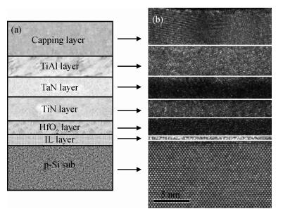
Fig. 1.
(a) Schematic diagram of the experimental structure. (b) HRTEM of the sample.
SEMICONDUCTOR TECHNOLOGY
Xueli Ma, Hong Yang, Wenwu Wang, Huaxiang Yin, Huilong Zhu, Chao Zhao, Dapeng Chen and Tianchun Ye
Corresponding author: Ma Xueli, Email:maxueli@ime.ac.cn; Ma Xueli, Email:maxueli@ime.ac.cn
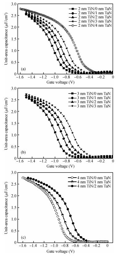
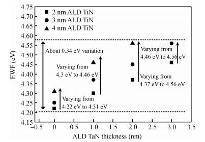
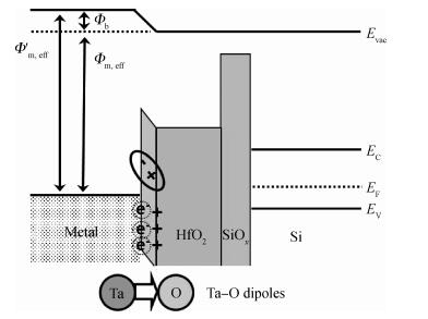
Abstract: We evaluated the TiN/TaN/TiAl triple-layer to modulate the effective work function (EWF) of a metal gate stack for the n-type metal-oxide-semiconductor (NMOS) devices application by varying the TiN/TaN thickness. In this paper, the effective work function of EWF ranges from 4.22 to 4.56 eV with different thicknesses of TiN and TaN. The thinner TiN and/or thinner in situ TaN capping, the closer to conduction band of silicon the EWF is, which is appropriate for 2-D planar NMOS. Mid-gap work function behavior is observed with thicker TiN, thicker in situ TaN capping, indicating a strong potential candidate of metal gate material for replacement gate processed three-dimensional devices such as FIN shaped field effect transistors. The physical understandings of the sensitivity of EWF to TiN and TaN thickness are proposed. The thicker TiN prevents the Al diffusion then induces the EWF to shift to mid-gap. However, the TaN plays a different role in effective work function tuning from TiN, due to the Ta-O dipoles formed at the interface between the metal gate and the high-k layer.
Keywords: TaN, TiAl, Ta-O dipole, effective work function
| [1] |
Robertson J. High dielectric constant gate oxides for metal oxide Si transistors. Rep Prog Phys, 2006, 69:327 doi: 10.1088/0034-4885/69/2/R02
|
| [2] |
De I, Johri D, Srivastava A, et al. Impact of gate work function on device performance at the 50 nm technology node. Solid-State Electron, 2000, 44:1077 doi: 10.1016/S0038-1101(99)00323-8
|
| [3] |
Chang L, Tang S, King T, et al. Gate length scaling and threshold voltage control of double-gate MOSFETs. Proceedings of IEEE International Electron Devices Meeting, 2000:719 http://ieeexplore.ieee.org/xpls/abs_all.jsp?arnumber=904419
|
| [4] |
Liu Y X, Kijima S, Sugimata E, et al. Investigation of the TiN gate electrode with tunable work function and its application for FinFET fabrication. IEEE Trans Nanotechnology, 2006, 5(6):723 doi: 10.1109/TNANO.2006.885035
|
| [5] |
Kamei T, Liu Y X, Endo K, et al. Experimental study of physical vapor deposited titanium nitride gate with an n+-polycrystalline silicon capping layer and its application to 20 nm fin-type double-gate metal-oxide-semiconductor field-effect transistors. Jpn J Appl Phys, 2011, 50:04DC14
|
| [6] |
Choi K, Wen H C, Alshareef H, et al. The effect of metal thickness, overlayer and high-k surface treatment on the effective work function of metal electrode. Proceedings of European Solid-State Device Research Conference, 2005:101 http://ieeexplore.ieee.org/xpl/abstractAuthors.jsp?reload=true&tp=&arnumber=1546595&contentType=Conference+Publications&sortType%3Dasc_p_Sequence%26filter%3DAND%28p_IS_Number%3A32983%29
|
| [7] |
Kesapragada S, Wang R, Liu D, et al. High-k/metal gate stacks in gate first and replacement gate schemes. Proceedings of Advanced Semiconductor Manufacturing Conference, 2010:256 http://ieeexplore.ieee.org/xpl/articleDetails.jsp?reload=true&arnumber=5551460&contentType=Conference+Publications
|
| [8] |
Heo S C, Choi C. Plasma atomic layer deposited TiN metal gate for three dimensional device applications:deposition temperature, capping metal and post annealing. Microelectron Eng, 2012, 94:11 doi: 10.1016/j.mee.2011.12.001
|
| [9] |
Lee S H, Choi R, Choi C. Effects of composition and thickness of TiN metal gate on the equivalent oxide thickness and flat-band voltage in metal oxide semiconductor devices. Microelectron Eng, 2013, 109:160 doi: 10.1016/j.mee.2013.03.056
|
| [10] |
Xiong K, Robertson J, Pourtois G, et al. Impact of incorporated Al on the TiN/HfO2 interface effective work function. J Appl Phys, 2008, 104:074501 doi: 10.1063/1.2986158
|
| [11] |
Arimura H, Haight R, Brown S L, et al. Temperature-dependent La-and Al-induced dipole behavior monitored by femtosecond pump/probe photoelectron spectroscopy. Appl Phys Lett, 2010, 96:132902 doi: 10.1063/1.3374883
|
| [12] |
Yang Z C, Huang A P, Yan L, et al. Role of interface dipole in metal gate/high-k effective work function modulation by aluminum incorporation. Appl Phys Lett, 2009, 94:252905 doi: 10.1063/1.3159830
|
| [13] |
Chen B, Jha R, Misra V. Work function tuning via interface dipole by ultrathin reaction layers using AlTa and AlTaN alloys. IEEE Electron Device Lett, 2006, 27(9):731 doi: 10.1109/LED.2006.880643
|
| [14] |
Kornblum L, Rothschild J A, Kauffmann Y, et al. Band offsets and Fermi level pinning at metal-Al2O3 interfaces. Phys Rev B, 2011, 84:155317 doi: 10.1103/PhysRevB.84.155317
|
| [15] |
Kornblum L, Meyler B, Salzman J, et al. The electrostatics of Ta2O5 in Si-based metal oxide semiconductor devices. J Appl Phys, 2013, 113:074102 doi: 10.1063/1.4792750
|
| [16] |
Cheng C L, Liu C W, Jeng J T. Work function tuning of the TixTayN metal gate electrode for advanced metal oxide semiconductor devices applications. Appl Phys Lett, 2007, 90:062114 doi: 10.1063/1.2472531
|
| [17] |
Ragnarsson L A, Chiarella T, Togo M, et al. Ultrathin EOT high-k/metal gate devices for future technologies:challenges, achievements and perspectives. Microelectron Eng, 2011, 88:1317 doi: 10.1016/j.mee.2011.03.121
|


Article views: 6985 Times PDF downloads: 404 Times Cited by: 0 Times
Received: 17 February 2014 Revised: 01 April 2014 Online: Published: 01 September 2014
| Citation: |
Xueli Ma, Hong Yang, Wenwu Wang, Huaxiang Yin, Huilong Zhu, Chao Zhao, Dapeng Chen, Tianchun Ye. An effective work-function tuning method of nMOSCAP with high-k/metal gate by TiN/TaN double-layer stack thickness[J]. Journal of Semiconductors, 2014, 35(9): 096001. doi: 10.1088/1674-4926/35/9/096001
****
X L Ma, H Yang, W W Wang, H X Yin, H L Zhu, C Zhao, D P Chen, T C Ye. An effective work-function tuning method of nMOSCAP with high-k/metal gate by TiN/TaN double-layer stack thickness[J]. J. Semicond., 2014, 35(9): 096001. doi: 10.1088/1674-4926/35/9/096001.

|
| [1] |
Robertson J. High dielectric constant gate oxides for metal oxide Si transistors. Rep Prog Phys, 2006, 69:327 doi: 10.1088/0034-4885/69/2/R02
|
| [2] |
De I, Johri D, Srivastava A, et al. Impact of gate work function on device performance at the 50 nm technology node. Solid-State Electron, 2000, 44:1077 doi: 10.1016/S0038-1101(99)00323-8
|
| [3] |
Chang L, Tang S, King T, et al. Gate length scaling and threshold voltage control of double-gate MOSFETs. Proceedings of IEEE International Electron Devices Meeting, 2000:719 http://ieeexplore.ieee.org/xpls/abs_all.jsp?arnumber=904419
|
| [4] |
Liu Y X, Kijima S, Sugimata E, et al. Investigation of the TiN gate electrode with tunable work function and its application for FinFET fabrication. IEEE Trans Nanotechnology, 2006, 5(6):723 doi: 10.1109/TNANO.2006.885035
|
| [5] |
Kamei T, Liu Y X, Endo K, et al. Experimental study of physical vapor deposited titanium nitride gate with an n+-polycrystalline silicon capping layer and its application to 20 nm fin-type double-gate metal-oxide-semiconductor field-effect transistors. Jpn J Appl Phys, 2011, 50:04DC14
|
| [6] |
Choi K, Wen H C, Alshareef H, et al. The effect of metal thickness, overlayer and high-k surface treatment on the effective work function of metal electrode. Proceedings of European Solid-State Device Research Conference, 2005:101 http://ieeexplore.ieee.org/xpl/abstractAuthors.jsp?reload=true&tp=&arnumber=1546595&contentType=Conference+Publications&sortType%3Dasc_p_Sequence%26filter%3DAND%28p_IS_Number%3A32983%29
|
| [7] |
Kesapragada S, Wang R, Liu D, et al. High-k/metal gate stacks in gate first and replacement gate schemes. Proceedings of Advanced Semiconductor Manufacturing Conference, 2010:256 http://ieeexplore.ieee.org/xpl/articleDetails.jsp?reload=true&arnumber=5551460&contentType=Conference+Publications
|
| [8] |
Heo S C, Choi C. Plasma atomic layer deposited TiN metal gate for three dimensional device applications:deposition temperature, capping metal and post annealing. Microelectron Eng, 2012, 94:11 doi: 10.1016/j.mee.2011.12.001
|
| [9] |
Lee S H, Choi R, Choi C. Effects of composition and thickness of TiN metal gate on the equivalent oxide thickness and flat-band voltage in metal oxide semiconductor devices. Microelectron Eng, 2013, 109:160 doi: 10.1016/j.mee.2013.03.056
|
| [10] |
Xiong K, Robertson J, Pourtois G, et al. Impact of incorporated Al on the TiN/HfO2 interface effective work function. J Appl Phys, 2008, 104:074501 doi: 10.1063/1.2986158
|
| [11] |
Arimura H, Haight R, Brown S L, et al. Temperature-dependent La-and Al-induced dipole behavior monitored by femtosecond pump/probe photoelectron spectroscopy. Appl Phys Lett, 2010, 96:132902 doi: 10.1063/1.3374883
|
| [12] |
Yang Z C, Huang A P, Yan L, et al. Role of interface dipole in metal gate/high-k effective work function modulation by aluminum incorporation. Appl Phys Lett, 2009, 94:252905 doi: 10.1063/1.3159830
|
| [13] |
Chen B, Jha R, Misra V. Work function tuning via interface dipole by ultrathin reaction layers using AlTa and AlTaN alloys. IEEE Electron Device Lett, 2006, 27(9):731 doi: 10.1109/LED.2006.880643
|
| [14] |
Kornblum L, Rothschild J A, Kauffmann Y, et al. Band offsets and Fermi level pinning at metal-Al2O3 interfaces. Phys Rev B, 2011, 84:155317 doi: 10.1103/PhysRevB.84.155317
|
| [15] |
Kornblum L, Meyler B, Salzman J, et al. The electrostatics of Ta2O5 in Si-based metal oxide semiconductor devices. J Appl Phys, 2013, 113:074102 doi: 10.1063/1.4792750
|
| [16] |
Cheng C L, Liu C W, Jeng J T. Work function tuning of the TixTayN metal gate electrode for advanced metal oxide semiconductor devices applications. Appl Phys Lett, 2007, 90:062114 doi: 10.1063/1.2472531
|
| [17] |
Ragnarsson L A, Chiarella T, Togo M, et al. Ultrathin EOT high-k/metal gate devices for future technologies:challenges, achievements and perspectives. Microelectron Eng, 2011, 88:1317 doi: 10.1016/j.mee.2011.03.121
|

 WeChat ID
Journal of Semiconductors © 2017 All Rights Reserved 京ICP备05085259号-2

 DownLoad:

