


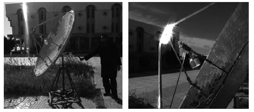
Fig. 1.
A photograph of the experimental setup.
SEMICONDUCTOR MATERIALS
Yacine Aoun1, Boubaker Benhaoua2, Brahim Gasmi3 and Said Benramache3, 4
Corresponding author: Yacine Aoun, E-mail: aounyacine07@gmail.com; Said Benramache, E-mail: saidzno2006@gmail.com
Abstract: Zinc oxide (ZnO) thin films were deposited on glass substrates by spray pyrolysis technique decomposition of zinc acetate dihydrate in an ethanol solution with 30 mL of deposition rate, the ZnO thin films were deposited at two different temperatures: 300 and 350 ℃. The substrates were heated using the solar cells method. The substrate was R217102 glass, whose size was 30 × 17.5 × 1 mm3. The films exhibit a hexagonal wurtzite structure with a strong (002) preferred orientation. The higher value of crystallite size is attained for sprayed films at 350 ℃, which is probably due to an improvement of the crystallinity of the films at this point. The average trans mittance of obtain films is about 90%-95%, as measured by a UV-vis analyzer. The band gap energy varies from 3.265 to 3.294 eV for the deposited ZnO thin film at 300 and 350 ℃, respectively. The electrical resistivity measured of our films are in the order 0.36 Ω·cm.
Keywords: ZnO, thin films, substrate temperature, spray pyrolysis technique
| [1] | |
| [2] | |
| [3] | |
| [4] | |
| [5] | |
| [6] | |
| [7] | |
| [8] | |
| [9] | |
| [10] | |
| [11] | |
| [12] | |
| [13] | |
| [14] | |
| [15] | |
| [16] | |
| [17] | |
| [18] | |
| [19] | |
| [20] | |
| [21] | |
| [22] | |
| [23] | |
| [24] | |
| [25] | |
| [26] |
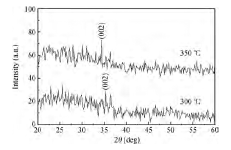
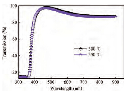
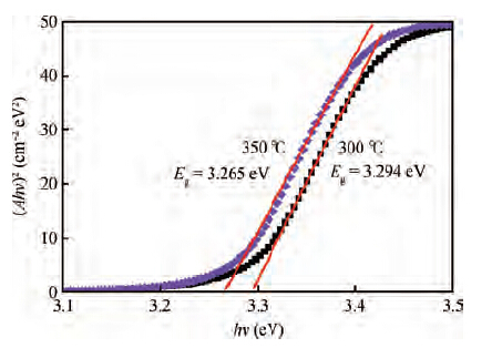
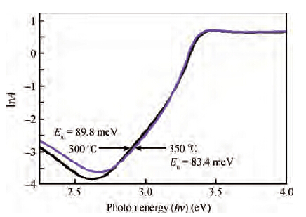
Table 1. Recapitulating measured values of Bragg angle (2$\theta )$, the inter planar spacing ($d)$, the full width at half-maximum (FWHM), the crystallite size ($G)$ and lattice parameters (cand $a)$ for ZnO thin films deposited at 300 and 350 C.
 DownLoad: CSV
Table 2. Recapitulating measured values of band gap energy ($E_{\rm g})$, Urbach energy ($E_{\rm u})$, and electrical resistivity ($\rho$) for ZnO thin films deposited at 300 and 350 C.
DownLoad: CSV
| [1] | |
| [2] | |
| [3] | |
| [4] | |
| [5] | |
| [6] | |
| [7] | |
| [8] | |
| [9] | |
| [10] | |
| [11] | |
| [12] | |
| [13] | |
| [14] | |
| [15] | |
| [16] | |
| [17] | |
| [18] | |
| [19] | |
| [20] | |
| [21] | |
| [22] | |
| [23] | |
| [24] | |
| [25] | |
| [26] |


Article views: 3667 Times PDF downloads: 41 Times Cited by: 0 Times
Received: 03 April 2014 Revised: Online: Published: 01 January 2015
| Citation: |
Yacine Aoun, Boubaker Benhaoua, Brahim Gasmi, Said Benramache. Structural, optical and electrical properties of zinc oxide thin films deposited by a spray pyrolysis technique[J]. Journal of Semiconductors, 2015, 36(1): 013002. doi: 10.1088/1674-4926/36/1/013002
****
Y Aoun, B Benhaoua, B Gasmi, S Benramache. Structural, optical and electrical properties of zinc oxide thin films deposited by a spray pyrolysis technique[J]. J. Semicond., 2015, 36(1): 013002. doi: 10.1088/1674-4926/36/1/013002.

|
| [1] | |
| [2] | |
| [3] | |
| [4] | |
| [5] | |
| [6] | |
| [7] | |
| [8] | |
| [9] | |
| [10] | |
| [11] | |
| [12] | |
| [13] | |
| [14] | |
| [15] | |
| [16] | |
| [17] | |
| [18] | |
| [19] | |
| [20] | |
| [21] | |
| [22] | |
| [23] | |
| [24] | |
| [25] | |
| [26] |

 WeChat ID
Journal of Semiconductors © 2017 All Rights Reserved 京ICP备05085259号-2


