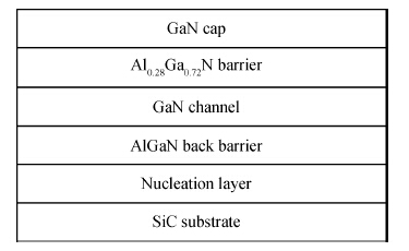
Fig. 1.
A schematic cross section of the AlGaN/GaN heterostructure with AlGaN back barrier.
SEMICONDUCTOR DEVICES
Chunjiang Ren, Hongchang Shen, Zhonghui Li, Tangsheng Chen, Bin Zhang and Tao Gao
Corresponding author: Chunjiang Ren, E-mail: rencj2010@sina.com
Abstract: 0.25 μm GaN HEMT with AlGaN back barrier for high power switch application has been presented. By introducing AlGaN back barrier, the buffer layer breakdown voltage for the metal-organic chemical vapor deposited AlGaN/GaN hetero-structure on 3-inch SiC substrate showed a considerable increment, which was nearly 4× and 2× of that for the conventional GaN buffer layer and GaN buffer layer with Fe doped, respectively. GaN switch HEMTs with source to drain spacing of 2, 2.5, 3, 3.5 and 4 μm were fabricated on the AlGaN/GaN epitaxial material with AlGaN back barrier and estimated off state power handling for the GaN switch HEMTs were 25.0, 46.2, 64.0, 79.2, and 88.4 W, respectively. A demonstrator DC-12 GHz GaN SPDT MMIC switch was designed in reflective series-shunt-shunt configuration based on the GaN HEMT, with a source to drain spacing of 2.5 μm. The developed SPDT MMIC switch showed a maximum insertion loss of 1.0 dB and a minimum isolation of 30 dB at a frequency range of DC-12 GHz. A power handling capability of 44.1 dBm was achieved at 10 GHz for the MMIC switch with continuous wave power compression measurement.
Keywords: AlGaN/GaN, HEMT, back barrier, MMIC, high power, switch
| [1] | |
| [2] | |
| [3] | |
| [4] | |
| [5] | |
| [6] | |
| [7] | |
| [8] | |
| [9] | |
| [10] | |
| [11] | |
| [12] | |
| [13] | |
| [14] | |
| [15] | |
| [16] |
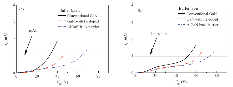
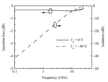
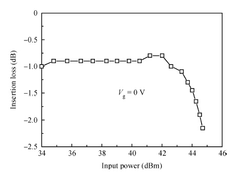
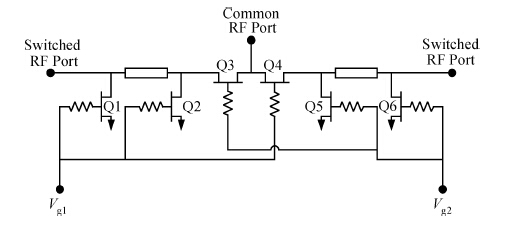
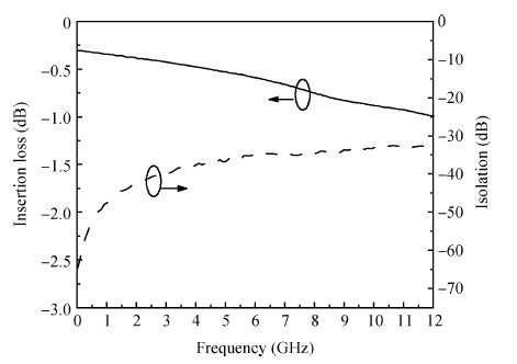
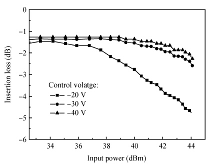
Table 2. Characteristics summary for the GaN switch HEMT with 2, 2.5, 3, 3.5, and 4 $\mu$m drain source spacing.
 DownLoad: CSV
| [1] | |
| [2] | |
| [3] | |
| [4] | |
| [5] | |
| [6] | |
| [7] | |
| [8] | |
| [9] | |
| [10] | |
| [11] | |
| [12] | |
| [13] | |
| [14] | |
| [15] | |
| [16] |


Article views: 4850 Times PDF downloads: 163 Times Cited by: 0 Times
Received: 18 March 2014 Revised: Online: Published: 01 January 2015
| Citation: |
Chunjiang Ren, Hongchang Shen, Zhonghui Li, Tangsheng Chen, Bin Zhang, Tao Gao. GaN HEMT with AlGaN back barrier for high power MMIC switch application[J]. Journal of Semiconductors, 2015, 36(1): 014008. doi: 10.1088/1674-4926/36/1/014008
****
C J Ren, H C Shen, Z H Li, T S Chen, B Zhang, T Gao. GaN HEMT with AlGaN back barrier for high power MMIC switch application[J]. J. Semicond., 2015, 36(1): 014008. doi: 10.1088/1674-4926/36/1/014008.

|
| [1] | |
| [2] | |
| [3] | |
| [4] | |
| [5] | |
| [6] | |
| [7] | |
| [8] | |
| [9] | |
| [10] | |
| [11] | |
| [12] | |
| [13] | |
| [14] | |
| [15] | |
| [16] |

 WeChat ID
Journal of Semiconductors © 2017 All Rights Reserved 京ICP备05085259号-2