


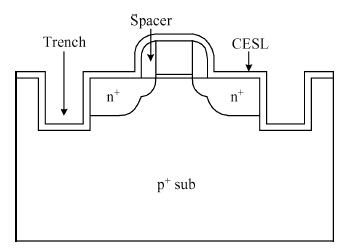
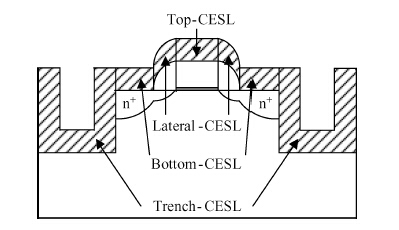
Fig. 1.
The schematic cross-section of the c-CESL strained NMOSFET with a trench-based structure.
SEMICONDUCTOR DEVICES
Di Zhao1, Qian Luo1, , Xiangzhan Wang1, Qi Yu1, Wei Cui2 and Kaizhou Tan2
Corresponding author: Qian Luo, E-mail: lourqian@uestc.edu.cn
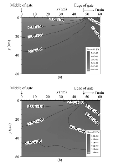
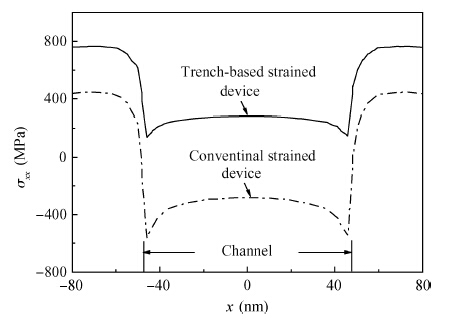
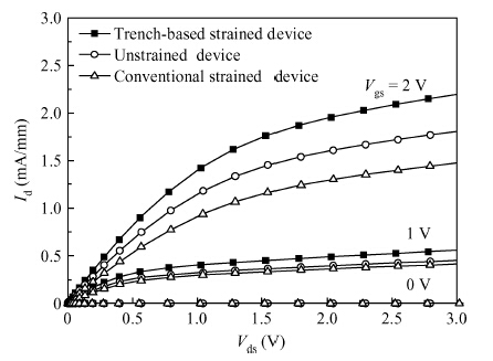
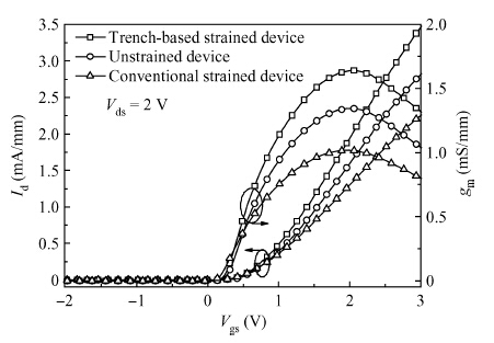
Abstract: A stress modulation technology using a trench-based structure for strained NMOSFET is reported in this paper. With this technology, NMOSFET can be improved by a compressive contact etch stop layer (CESL), whereas the traditional CESL-strained NMOSFET requires a tensile one. To confirm this idea, a 95-nm-gate device with a-2.5 GPa strained CESL is simulated to investigate the effects of the trench-based structure on channel stress. It is demonstrated that the average longitudinal channel stress is transformed from-333 into 256 MPa, which leads to a significant improvement of the device's I-V performance. For strained CMOS, this approach provides a potential alternative besides dual stress liner technology.
Keywords: CESL, trench, strained NMOSFET, SiN
| [1] | |
| [2] | |
| [3] | |
| [4] | |
| [5] | |
| [6] | |
| [7] | |
| [8] | |
| [9] | |
| [10] | |
| [11] |
| [1] | |
| [2] | |
| [3] | |
| [4] | |
| [5] | |
| [6] | |
| [7] | |
| [8] | |
| [9] | |
| [10] | |
| [11] |


Article views: 3381 Times PDF downloads: 28 Times Cited by: 0 Times
Received: 30 May 2014 Revised: Online: Published: 01 January 2015
| Citation: |
Di Zhao, Qian Luo, Xiangzhan Wang, Qi Yu, Wei Cui, Kaizhou Tan. Performance enhancement of c-CESL-strained 95-nm-gate NMOSFET usingtrench-based structure[J]. Journal of Semiconductors, 2015, 36(1): 014010. doi: 10.1088/1674-4926/36/1/014010
****
D Zhao, Q Luo, X Z Wang, Q Yu, W Cui, K Z Tan. Performance enhancement of c-CESL-strained 95-nm-gate NMOSFET usingtrench-based structure[J]. J. Semicond., 2015, 36(1): 014010. doi: 10.1088/1674-4926/36/1/014010.

|
| [1] | |
| [2] | |
| [3] | |
| [4] | |
| [5] | |
| [6] | |
| [7] | |
| [8] | |
| [9] | |
| [10] | |
| [11] |

 WeChat ID
Journal of Semiconductors © 2017 All Rights Reserved 京ICP备05085259号-2

 DownLoad:

