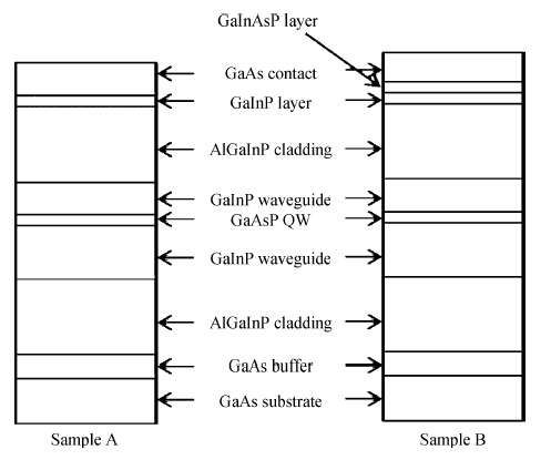
Fig. 1.
Schematic structure of LDs for samples A and B.
SEMICONDUCTOR DEVICES
Zhen Zhu1, 2, , Xin Zhang2, Peixu Li2, Gang Wang1 and Xiangang Xu2, 3
Corresponding author: Zhen Zhu, E-mail: zhuzhen2003@163.com
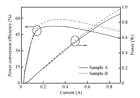
Abstract: GaInAsP layers and GaAsP/ (Al) GaInP laser diodes (LDs) have been grown on GaAs substrates by metalorganic chemical vapor deposition. The GaInAsP layer, which is lattice matched to GaAs, has an intermediate band gap between Ga0.5In0.5P and GaAs. The GaInP/GaAs heterojunction spikes, especially in the valence band, can be suppressed by introducing this thin GaInAsP layer into the heterostructure interface. The 808 nm GaAsP/ (Al) GaInP LDs with GaInAsP intermediate layer show a reduced operating voltage compared to the conventional LDs with abrupt GaInP/GaAs interface due to the enhanced hole injection. As a result, the power conversion efficiency is improved from 52% to 60% at 350 mW output power. At high current injection, the LD with GaInAsP intermediate layer has higher light power owing to the decreased joule heating.
Keywords: MOCVD, GaInAsP layer, heterojunction, voltage reduction
| [1] | |
| [2] | |
| [3] | |
| [4] | |
| [5] | |
| [6] | |
| [7] | |
| [8] | |
| [9] | |
| [10] | |
| [11] |
| [1] | |
| [2] | |
| [3] | |
| [4] | |
| [5] | |
| [6] | |
| [7] | |
| [8] | |
| [9] | |
| [10] | |
| [11] |


Article views: 3742 Times PDF downloads: 50 Times Cited by: 0 Times
Received: 19 June 2014 Revised: Online: Published: 01 January 2015
| Citation: |
Zhen Zhu, Xin Zhang, Peixu Li, Gang Wang, Xiangang Xu. Voltage reduction of 808 nm GaAsP/(Al)GaInP laser diodes with GaInAsP intermediate layer[J]. Journal of Semiconductors, 2015, 36(1): 014011. doi: 10.1088/1674-4926/36/1/014011
****
Z Zhu, X Zhang, P X Li, G Wang, X G Xu. Voltage reduction of 808 nm GaAsP/(Al)GaInP laser diodes with GaInAsP intermediate layer[J]. J. Semicond., 2015, 36(1): 014011. doi: 10.1088/1674-4926/36/1/014011.

|
| [1] | |
| [2] | |
| [3] | |
| [4] | |
| [5] | |
| [6] | |
| [7] | |
| [8] | |
| [9] | |
| [10] | |
| [11] |

 WeChat ID
Journal of Semiconductors © 2017 All Rights Reserved 京ICP备05085259号-2

 DownLoad: