


Fig. 1.
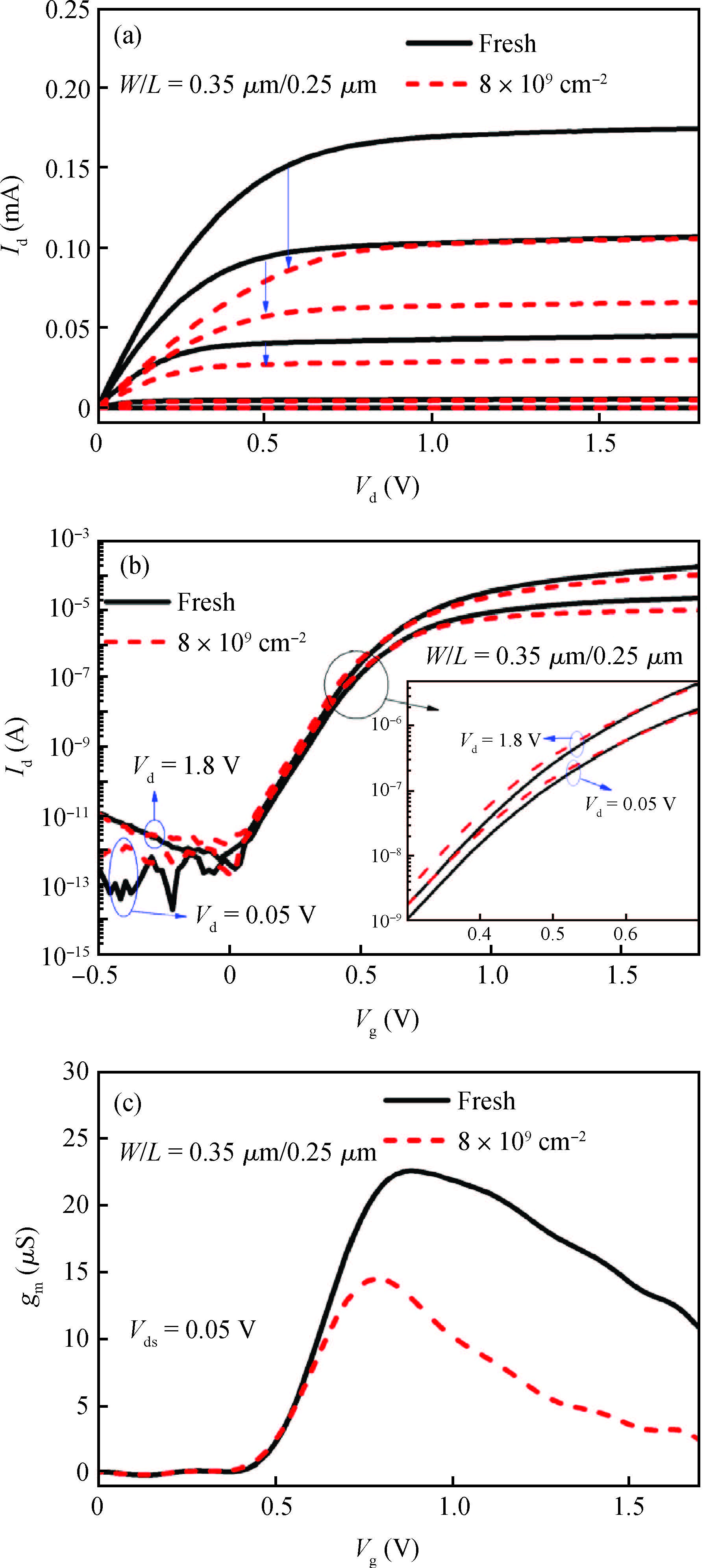
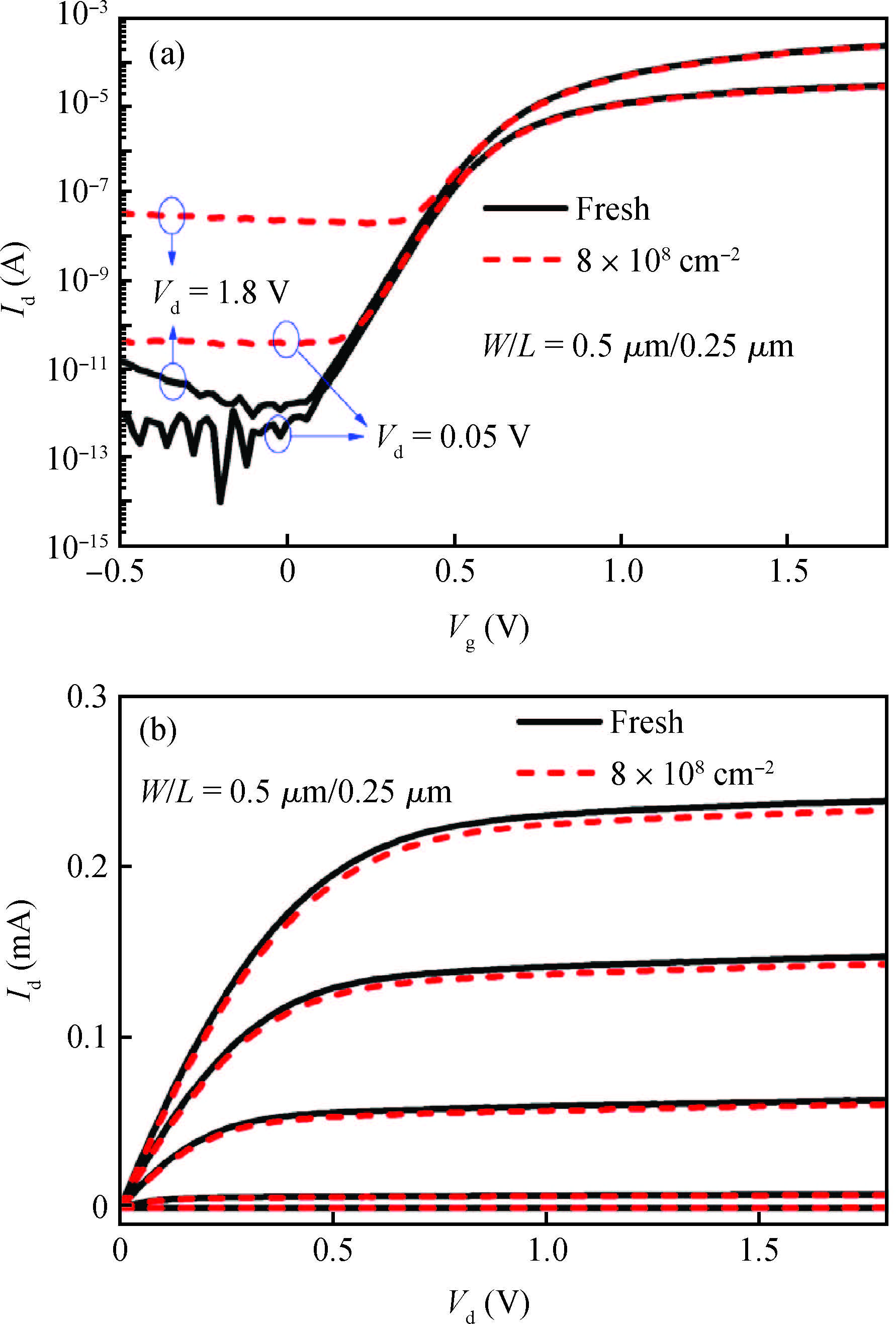
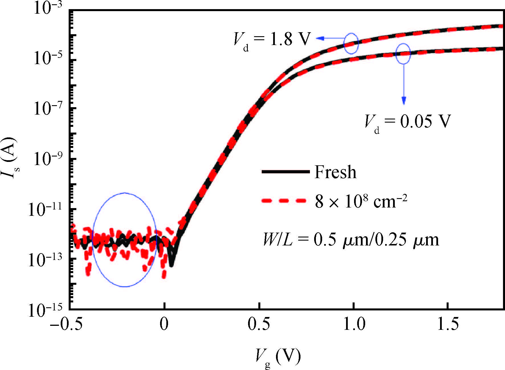
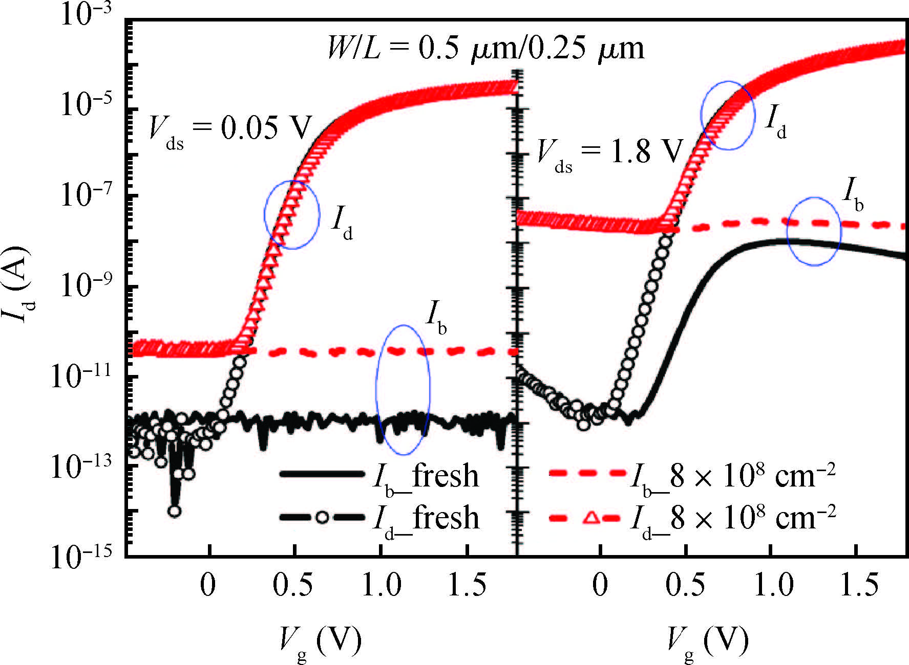
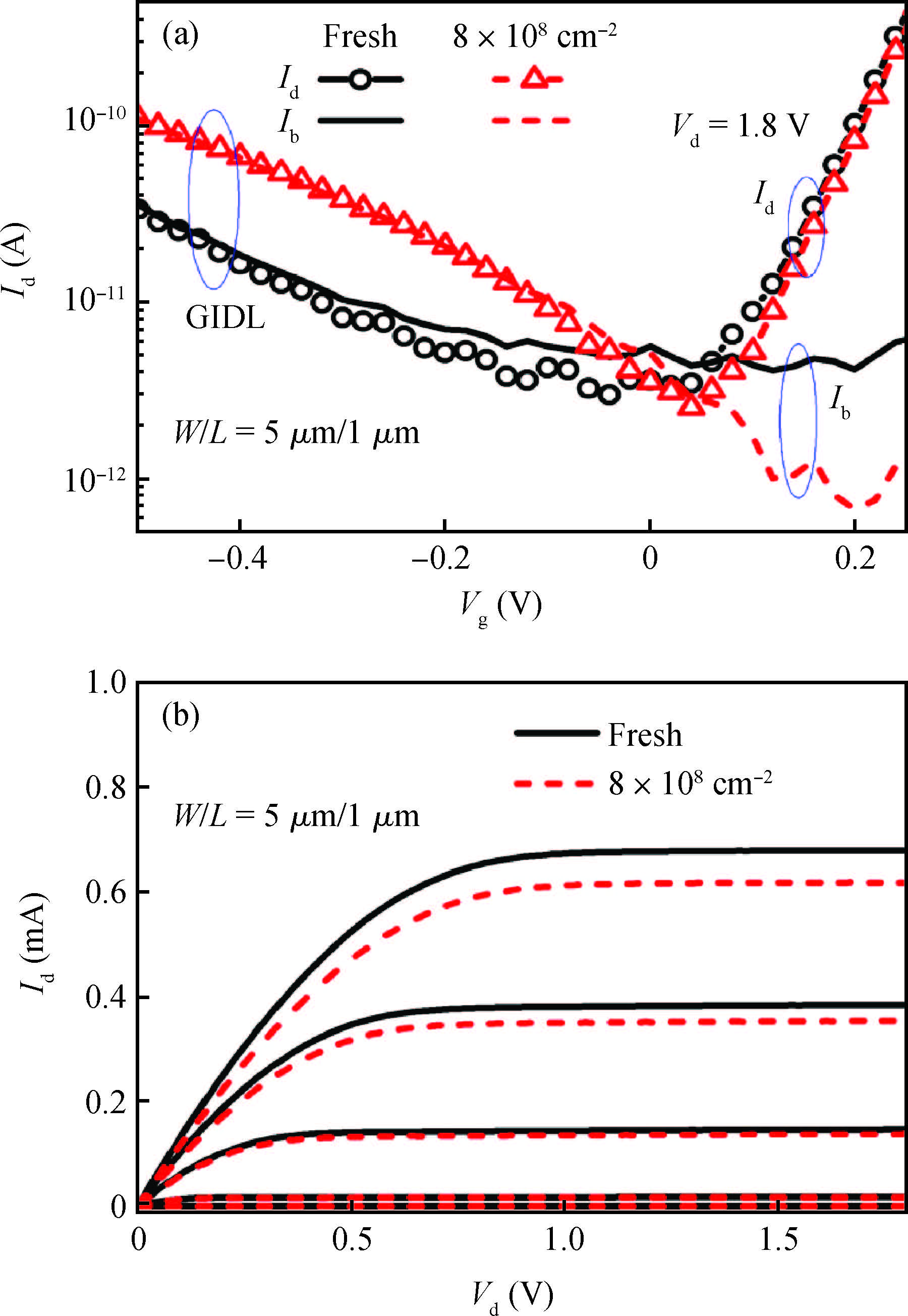
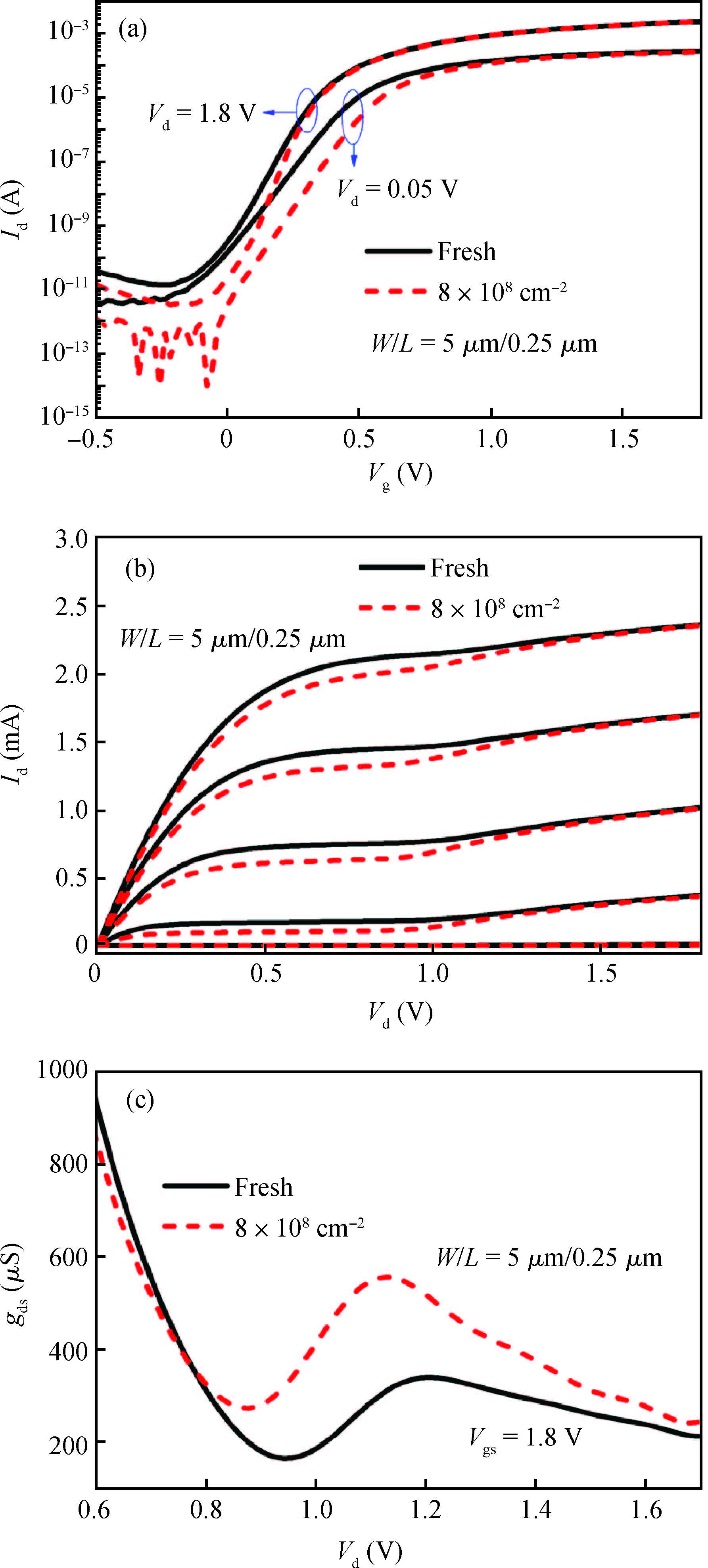
(Color online) The electrical characteristics of BC-PDSOI device before and after heavy ion exposure. (a) Output characteristics. (b) Transfer characteristics. (c) Transconductance.
SEMICONDUCTOR DEVICES
Weikang Wu, Xia An, Fei Tan, Hui Feng, Yehua Chen, Jingjing Liu, Xing Zhang and Ru Huang
Corresponding author: An Xia, Email: anxia@ime.pku.edu.cn; Huang Ru, Email: ruhuang@pku.edu.cn
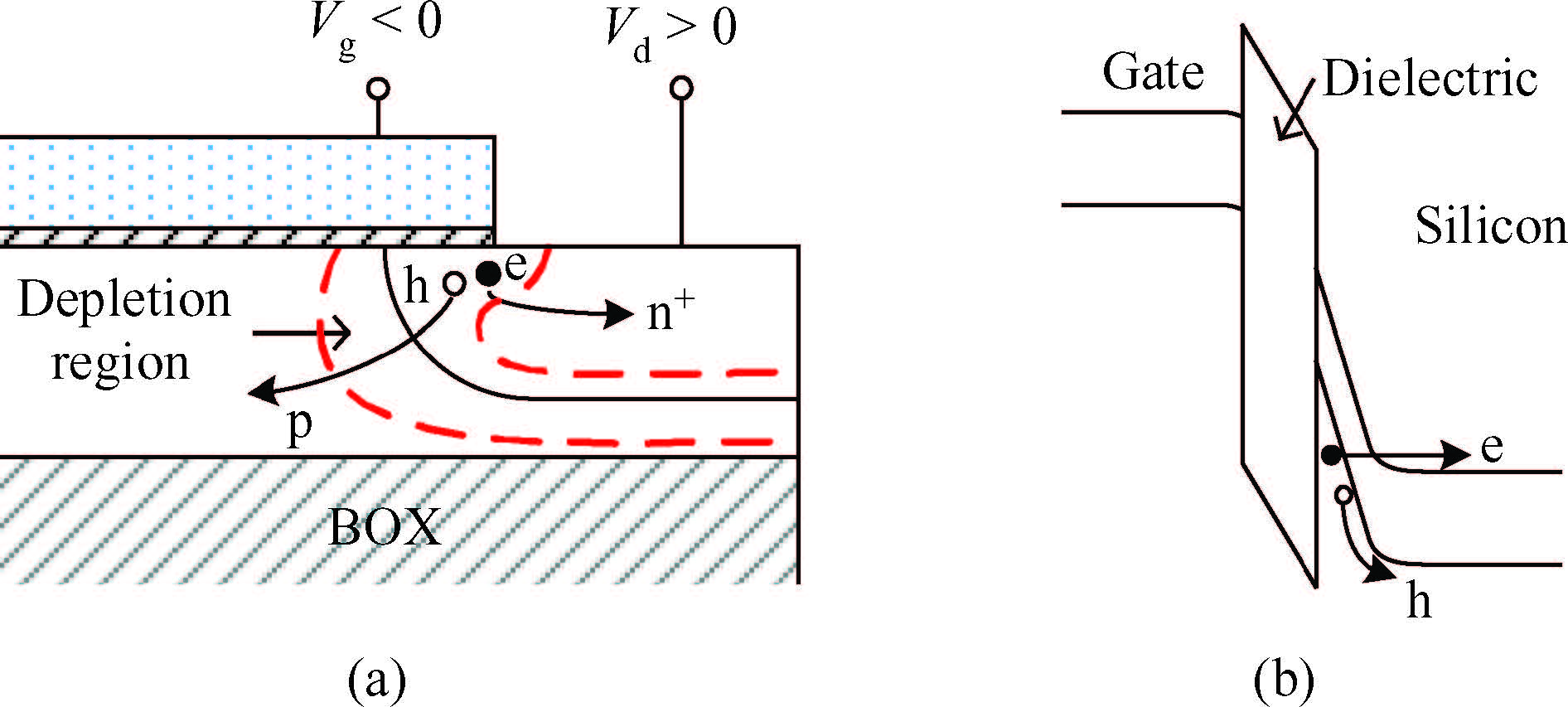
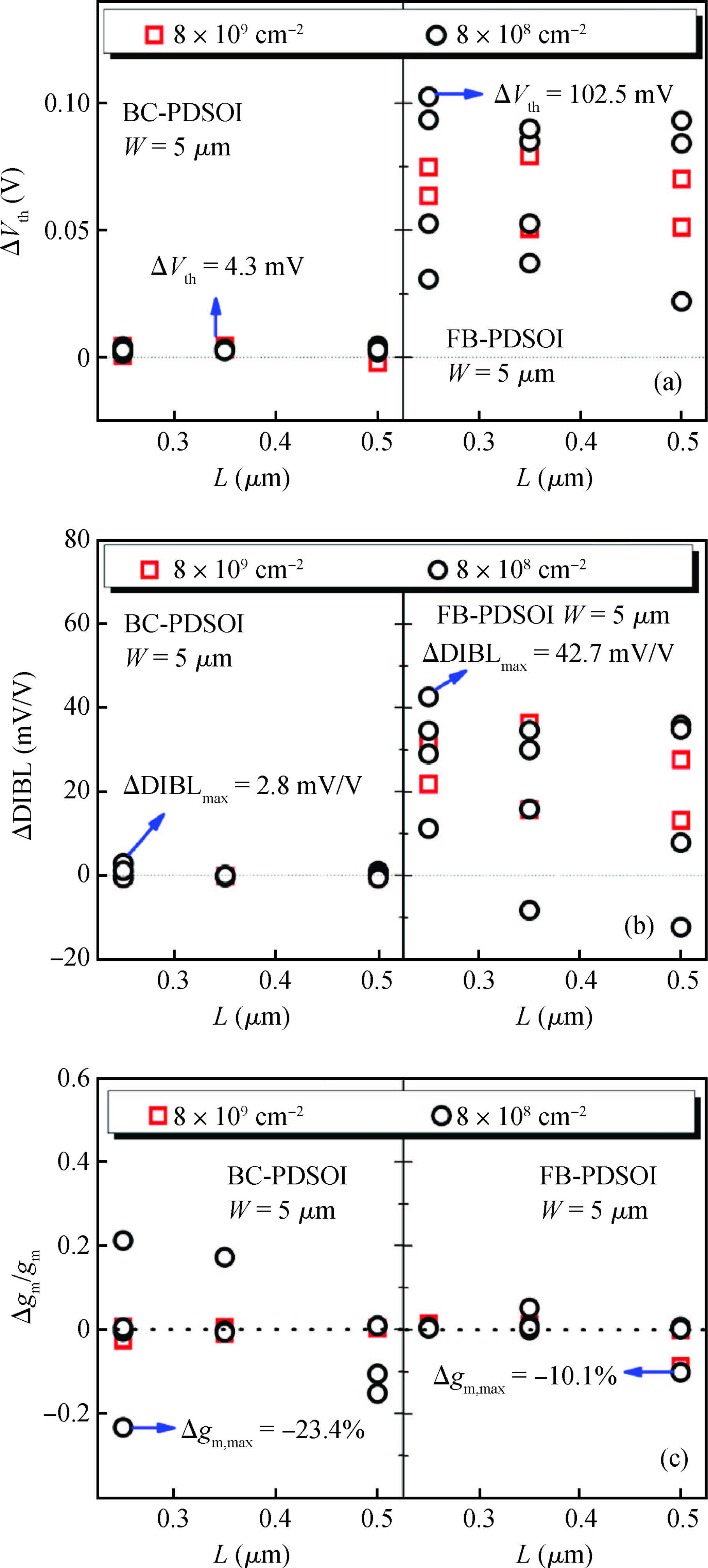
Abstract: The effects of the physical damages induced by heavy ion irradiation on the performance of partially-depleted SOI devices are experimentally investigated. After heavy ion exposure, different degradation phenomena are observed due to the random strike of heavy ions. A decrease of the saturation current and transconductance, and an enhanced gate-induced drain leakage current are observed, which are mainly attributed to the displacement damages that may be located in the channel, the depletion region of the drain/body junction or the gate-to-drain overlap region. Further, PDSOI devices with and without body contact are compared, which reveals the differences in the threshold voltage shift, the drain-induced barrier lowing effect, the transconductance and the kink effect. The results may provide a guideline for radiation hardened design.
Keywords: heavy ion, displacement damages, PDSOI, performance degradation
| [1] | |
| [2] | |
| [3] | |
| [4] | |
| [5] | |
| [6] | |
| [7] | |
| [8] | |
| [9] | |
| [10] | |
| [11] | |
| [12] | |
| [13] | |
| [14] | |
| [15] | |
| [16] | |
| [17] | |
| [18] | |
| [19] | |
| [20] |
| [1] | |
| [2] | |
| [3] | |
| [4] | |
| [5] | |
| [6] | |
| [7] | |
| [8] | |
| [9] | |
| [10] | |
| [11] | |
| [12] | |
| [13] | |
| [14] | |
| [15] | |
| [16] | |
| [17] | |
| [18] | |
| [19] | |
| [20] |


Article views: 3811 Times PDF downloads: 31 Times Cited by: 0 Times
Received: 11 June 2015 Revised: Online: Published: 01 November 2015
| Citation: |
Weikang Wu, Xia An, Fei Tan, Hui Feng, Yehua Chen, Jingjing Liu, Xing Zhang, Ru Huang. Effects of heavy ion irradiation on ultra-deep-submicron partially-depleted SOI devices[J]. Journal of Semiconductors, 2015, 36(11): 114004. doi: 10.1088/1674-4926/36/11/114004
****
W K Wu, X An, F Tan, H Feng, Y H Chen, J J Liu, X Zhang, R Huang. Effects of heavy ion irradiation on ultra-deep-submicron partially-depleted SOI devices[J]. J. Semicond., 2015, 36(11): 114004. doi: 10.1088/1674-4926/36/11/114004.

|
| [1] | |
| [2] | |
| [3] | |
| [4] | |
| [5] | |
| [6] | |
| [7] | |
| [8] | |
| [9] | |
| [10] | |
| [11] | |
| [12] | |
| [13] | |
| [14] | |
| [15] | |
| [16] | |
| [17] | |
| [18] | |
| [19] | |
| [20] |

 WeChat ID
Journal of Semiconductors © 2017 All Rights Reserved 京ICP备05085259号-2

 DownLoad:

