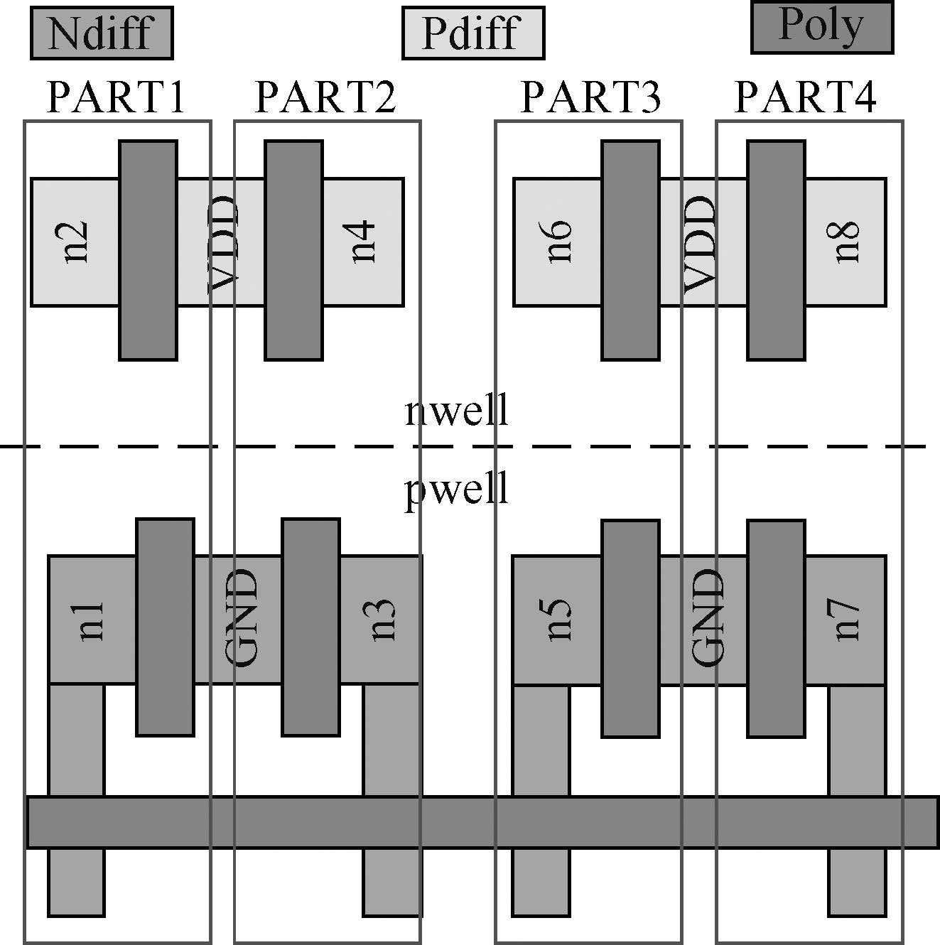
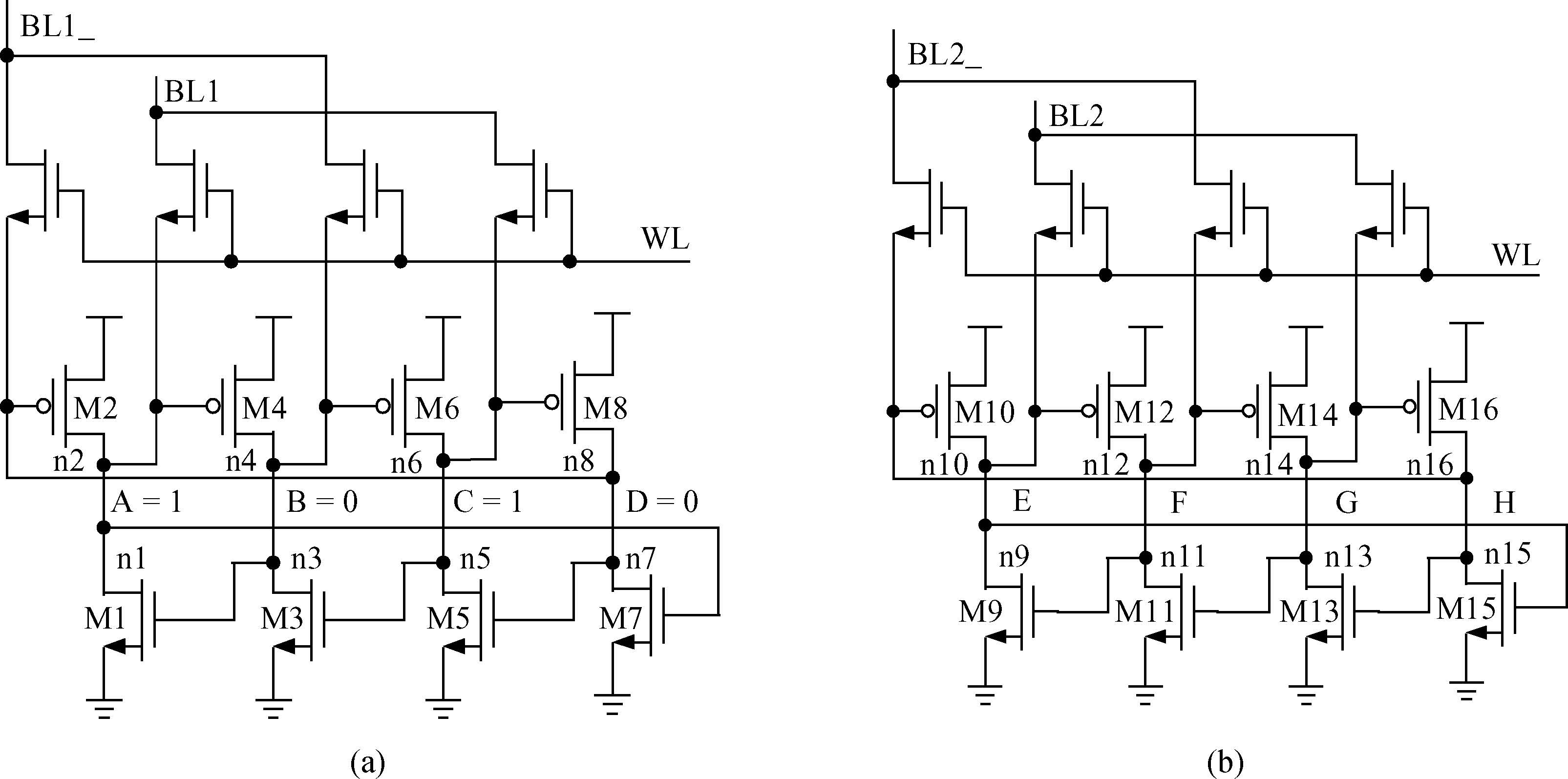
Processing math: 100%
J. Semicond. > 2015, Volume 36 > Issue 11 > 115007

SEMICONDUCTOR INTEGRATED CIRCUITS

A four-interleaving HBD SRAM cell based on dual DICE for multiple node collection mitigation

Lin Liu1, , Suge Yue1, 2 and Shijin Lu1

+ Author Affiliations

 Corresponding author: Liu Lin, Email: liulin19830703@126.com

DOI: 10.1088/1674-4926/36/11/115007

PDF

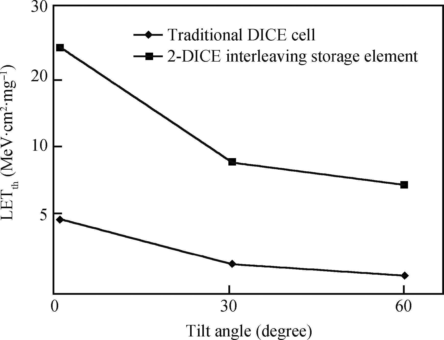
Abstract: A 4-interleaving cell of 2-dual interlocked cells (DICE) is proposed, which reduces single event induced multiple node collection between the sensitive nodes of sensitive pairs in a DICE storage cell in 65 nm technology. The technique involves the 4-interleaving of dual DICE cells at a layout level to meet the required spacing between sensitive nodes in an area-efficient manner. Radiation experiments using a 65 nm CMOS test chip demonstrate that the LETth of our 4-interleaving cell of dual DICE encounters are almost 4× larger and the SEU cross section per bit for our proposed dual DICE design is almost two orders of magnitude less compared to the reference traditional DICE cell.

Key words: single event upset (SEU)hardened-by-design (HBD)multi-node upset (MNU)

Single event upset (SEU) hardening has become more complex due to the shrinking of device sizes and the increase in circuit density. Conventional hardened-by-design (HBD) techniques to mitigate soft errors,such as triple modular redundancy (TMR) or dual inter locked cell (DICE),are based on redundancy,requiring that an incident single-event (SE) ion affects only one circuit node. However,such designs are vulnerable to ion hits that result in multiple nodes collecting charge,as shown by Olson et al.[1] and Amusan et al.[2]. For deep sub-micron technologies,the proximity of circuit nodes may result in charge collection at multiple nodes from a single ion strike[3, 4].

One hardened-by-design technique to help mitigate multiple node collection is guard contacts[5, 6, 7]. The use of well contacts and a guard ring is effective in mitigating parasitic PNP bipolar effects[6],but it is limited to the struck devices only. Guard and well contacts are used to help mitigate bipolar conduction by stabilizing well potential during a single event effect (SEE)[6, 7],but they are only useful for reducing multi-node charge collection effects associated with NMOS sensitive node pairs or PMOS sensitive node pairs in the same single well.

Another hardened-by-design technique to help mitigate multiple node collection is the 2-interleaving storage element[8, 9]. The technique of the 2-interleaving storage element is only effective in separating NMOS sensitive node pairs or PMOS sensitive node pairs,which cannot separate the NMOS or PMOS node pairs.

In this paper,three-dimensional (3-D) technology computer aided design (TCAD) simulation shows that the most vulnerable node pairs of a DICE SRAM cell are the PMOS-NMOS sensitive node pairs in different wells other than the NMOS sensitive node pairs or PMOS sensitive node pairs in the same single well. Then a 4-interleaving cell of dual DICE is designed as an effective method to separate all the sensitive node pairs in an area-efficient manner. The 3D TCAD simulation and the radiation experiment both show that the new 4-interleaving cell of dual DICE significantly improve soft error resilience compared to the reference SRAM DICE cell.

The DICE is a storage element that relies on dual redundancy of internal circuit nodes to achieve soft-error resilience [Calin 96]. A DICE storage element is immune to single event upsets affecting single circuit nodes,but is vulnerable to single event multiple upsets affecting multiple circuit nodes [Baze 08]. The basic 12-transistor DICE storage element is shown in Figure1.

Figure  1.  Schematic of the DICE cell. (a) DICE1. (b) DICE2.

When the drain contact node of an "off" transistor in the DICE design,e.g.,the drain contact node n1 in Figure1,is hit by a particle,the circuit node connected to this drain contact node,e.g.,circuit node A,can temporarily switch its logic state. This can turn off a previously ``on'' transistor,e.g.,M7,and turn on a previously "off" transistor,e.g.,M4,causing the following behaviors in the remaining circuit nodes:

(1) Circuit node B is now driven by both "on" transistors M3 and M4. This results in voltage contention at circuit node B.

(2) The change in the voltage of circuit node B reduces the current drive of M6. As a result,node C is now weakly driven by M6. (3) Circuit node D is now left floating (M7 and M8 are "off").

If no other circuit node in the DICE storage element is affected by the single event,circuit node A will eventually recover its original state,and the storage element will continue to produce correct outputs. However,if an additional drain contact node of an "off" transistor is hit by the same single event,an upset may be induced in the storage element.

Recent studies have shown that bipolar amplification between PMOS sensitive node pairs due to the n-well potential collapse and charge diffusion between sensitive node pairs in the case of a single strike are the main charge sharing mechanisms[4, 10]. Dodd et al. have shown that parasitic bipolar conduction may induce multiple node collection between PMOS-NMOS transistors. Considering all the charge collection mechanisms,the sensitive node pairs in a DICE cell at different initial states are shown in Table1.

Table  1.  Sensitive node pair in DICE1 cell with different layout.
DownLoad: CSV  | Show Table

Due to shrinking device sizes,the sensitive node pairs in a traditional DICE cell are so close to each other that the traditional DICE cell is more sensitive to SEU. As we discussed in Section 2,the distances between most of the sensitive node pairs in a traditional DICE cell are less than 1 μm. Especially,the sensitive NMOS--PMOS node pairs are (n5,n4),(n3,n2) and (n7,n6). At the same time,a different sensitive node pair of the DICE cell has a different upset mechanism,so single event upset hardening has become more complex for the DICE cell.

In this paper,a 4-interleaving cell of a dual DICE layout technique is proposed to reduce susceptibility to upsets for DICE elements in 65 nm technology. Figure2 shows a traditional DICE cell layout. First,we divide the traditional DICE layout into four parts,and make a copy to have two of the same DICE layouts: DICE1 and DICE2. Here we make the DICE1 cell the target cell. For each sensitive node pair in DICE1 layout that can be simultaneously ``affected'' by a single event,we place parts of another DICE layout (DICE2) between the sensitive node pair of DICE1.

Figure  2.  Layout configuration for a SRAM DICE cell.

Figure3 shows the 4-interleaving implementation of dual DICE implementation for the dual DICE storage element. Table1 shows the distances of all the sensitive node pairs in the traditional DICE layout and in the 4-interleaving cell layout of dual DICE. We can see that 4-interleaving cell layout of dual DICE hardened design method effectively separate all the sensitive node pairs,and effectively increase the distances of all the sensitive node pairs in DICE1.

Figure  3.  Layout configuration for the new 2-DICE interleaving cell.

Accurate single event simulations can provide effective quantitative assessment of a 4-interleaving cell layout of dual DICE hardened design. We have used the tool Cogenda[11] which accurately simulates single event charge distribution and charge collection while fully accounting for layout,substrate,and circuit details. This single event simulation tool provides accuracy similar to a full 3D TCAD device simulation,and is fast enough to run a very large number of single event experiments as required for cross-section and LET threshold prediction.

To evaluate the dual DICE 4-interleaving storage element layout and compare it to the traditional DICE cell layout,we implemented two layouts in 65 nm CMOS technology for the basic DICE circuit (Figure1),traditional DICE cell layout (Figure2) and the dual DICE 4-interleaving storage element layout (Figure3). Note that both layouts use exactly the same device sizing. Figure4 shows the 3D model of the simulated dual DICE 4-interleaving storage element.

Figure  4.  3D model of the simulated 2-DICE interleaving storage element.

As shown in Figure5,the lowest LET upset threshold for 4-interleaving cell layout of dual DICE is almost an order of magnitude larger than the lowest LET upset threshold for DICE. These simulation results also indicate that the sensitive NMOS--PMOS node pairs: n2--n3,n4--n5 and n6--n7 are the most vulnerable sensitive node pairs in both the traditional DICE cell and the 4-interleaving cell layout of dual DICE.

Figure  5.  LET upset threshold as a function of tilt angle for 2-DICE interleaving storage element at an azimuth angle of 320,and for traditional DICE cell at an azimuth angle of 300.

While the simulations presented here are relatively limited in scope,they show the effectiveness of the dual DICE 4-interleaving layout hardened design method and quantify the reduction in LET upset threshold for the 4-interleaving cell layout of dual DICE compared to the traditional DICE.

To evaluate the effectiveness of the 4-interleaving cell layout of dual DICE,we implemented two 128 kb SRAM circuits,with the traditional DICE and the 4-interleaving cell layout of dual DICE respectively to be the SRAM cells,in 65-nm CMOS technology. The layout of it is shown in Figure6.

Figure  6.  The layout of the 128 kb SRAM circuit with 2-DICE interleaving design method.

Radiation experiment test conditions for the two SRAM circuits are exactly the same: the test mode is 55H,the circuit's array power is 1.2 V. All the heavy ions are at an angle of incidence tilt = 0,azimuth = 0. The heavy ion results of the two 128 kb SRAMs,with the traditional DICE and the 4-interleaving cell layout of dual DICE,respectively to be the SRAM cells,are summarized in Table2.

Table  2.  Heavy ion results.
DownLoad: CSV  | Show Table

The radiation experiment result shows that the dual DICE 4-interleaving SRAM have no upset with both F and Cl to be the incident ion. The LETth of the dual DICE 4-interleaving SRAM is more than 20 MeVcm2/mg; while we can see the traditional DICE SRAM upsets with F to be the incident ion,so the LETth of the traditional DICE SRAM is less than 5~MeVcm2/mg. As shown in Table2,the SEU cross section per bit for the traditional DICE SRAM is almost two orders of magnitude larger than SEU cross section per bit for the 2-DICE interleaving SRAM. The results of the heavy-ion testing generally support the simulation results.

The SEU response of the two different cell layouts suggests that the 4-interleaving cell of the dual DICE layout technique is effective to reduce susceptibility to upsets for DICE elements. By interleaving dual DICE cells,the separation of sensitive nodes can be accomplished without the arbitrary wasting of area to space the nodes sufficiently apart.

3D TCAD simulations are used to reveal that the sensitive PMOS--NMOS node pairs in different wells has become the most vulnerable sensitive node pairs,with both in a traditional DICE layout.

In this paper,a dual-DICE design is proposed,which interleaves 4 parts of two DICE storage cells to make them more resistant to multiple node upsets caused by a single event. The technique involves the 4-interleaving of dual DICE cells at a layout level to meet the required spacing between sensitive nodes in an area-efficient manner. By interleaving dual DICE cells,the separation of sensitive nodes can be accomplished without the arbitrary wasting of area to space the nodes sufficiently apart.

The dual DICE 4-interleaving layout hardened design enables the design of the 4-interleaving cell layout of dual DICE with significantly improved soft error resilience compared to our reference traditional DICE SRAM cell. The 4-interleaving cell layout of dual DICE retains the circuit design of DICE,but uses a new layout design. The radiation experiment results using 65nm test circuits demonstrate that the SEU cross section per bit for our dual DICE 4-interleaving SRAM is almost two orders of magnitude less than our reference traditional DICE SRAM. This improvement comes at a negligible power and performance cost compared to DICE,and the 4-interleaving cell layout of dual DICE is a 2 bits storage element,so the area cost is acceptable.


[1]
[2]
[3]
[4]
[5]
[6]
[7]
[8]
[9]
[10]
[11]
Fig. 1.  Schematic of the DICE cell. (a) DICE1. (b) DICE2.

Fig. 2.  Layout configuration for a SRAM DICE cell.

Fig. 3.  Layout configuration for the new 2-DICE interleaving cell.

Fig. 4.  3D model of the simulated 2-DICE interleaving storage element.

Fig. 5.  LET upset threshold as a function of tilt angle for 2-DICE interleaving storage element at an azimuth angle of 320,and for traditional DICE cell at an azimuth angle of 300.

Fig. 6.  The layout of the 128 kb SRAM circuit with 2-DICE interleaving design method.

Table 1.   Sensitive node pair in DICE1 cell with different layout.

DownLoad: CSV

Table 2.   Heavy ion results.

DownLoad: CSV
[1]
[2]
[3]
[4]
[5]
[6]
[7]
[8]
[9]
[10]
[11]
1

An advanced SEU tolerant latch based on error detection

Hui Xu, Jianwei Zhu, Xiaoping Lu, Jingzhao Li

Journal of Semiconductors, 2018, 39(5): 055003. doi: 10.1088/1674-4926/39/5/055003

2

Detection of lead ions with AlGaAs/InGaAs pseudomorphic high electron mobility transistor

Jiqiang Niu, Yang Zhang, Min Guan, Chengyan Wang, Lijie Cui, et al.

Journal of Semiconductors, 2016, 37(11): 114003. doi: 10.1088/1674-4926/37/11/114003

3

Design of current mirror integration ROIC for snapshot mode operation

Hari Shanker Gupta, A S Kiran Kumar, M. Shojaei Baghini, Subhananda Chakrabarti, Sanjeev Mehta, et al.

Journal of Semiconductors, 2016, 37(10): 105001. doi: 10.1088/1674-4926/37/10/105001

4

Modeling and analysis of the HPM pulse-width upset effect on CMOS inverter

Xinhai Yu, Changchun Chai, Liping Qiao, Yintang Yang, Yang Liu, et al.

Journal of Semiconductors, 2015, 36(5): 054011. doi: 10.1088/1674-4926/36/5/054011

5

Single event soft error in advanced integrated circuit

Yuanfu Zhao, Suge Yue, Xinyuan Zhao, Shijin Lu, Qiang Bian, et al.

Journal of Semiconductors, 2015, 36(11): 111001. doi: 10.1088/1674-4926/36/11/111001

6

Multi-bit upset aware hybrid error-correction for cache in embedded processors

Jiaqi Dong, Keni Qiu, Weigong Zhang, Jing Wang, Zhenzhen Wang, et al.

Journal of Semiconductors, 2015, 36(11): 114006. doi: 10.1088/1674-4926/36/11/114006

7

Impacts of test factors on heavy ion single event multiple-cell upsets in nanometer-scale SRAM

Yinhong Luo, Fengqi Zhang, Hongxia Guo, Yao Xiao, Wen Zhao, et al.

Journal of Semiconductors, 2015, 36(11): 114009. doi: 10.1088/1674-4926/36/11/114009

8

Modeling and simulation of single-event effect in CMOS circuit

Suge Yue, Xiaolin Zhang, Yuanfu Zhao, Lin Liu

Journal of Semiconductors, 2015, 36(11): 111002. doi: 10.1088/1674-4926/36/11/111002

9

Laser SEU sensitivity mapping of deep submicron CMOS SRAM

Yongtao Yu, Guoqiang Feng, Rui Chen, Jianwei Han

Journal of Semiconductors, 2014, 35(6): 064011. doi: 10.1088/1674-4926/35/6/064011

10

Impact of temperature on single event upset measurement by heavy ions in SRAM devices

Tianqi Liu, Chao Geng, Zhangang Zhang, Fazhan Zhao, Song Gu, et al.

Journal of Semiconductors, 2014, 35(8): 084008. doi: 10.1088/1674-4926/35/8/084008

11

Design and implementation of a programming circuit in radiation-hardened FPGA

Wu Lihua, Han Xiaowei, Zhao Yan, Liu Zhongli, Yu Fang, et al.

Journal of Semiconductors, 2011, 32(8): 085012. doi: 10.1088/1674-4926/32/8/085012

12

SRAM single event upset calculation and test using protons in the secondary beam in the BEPC

Wang Yuanming, Guo Hongxia, Zhang Fengqi, Zhang Keying, Chen Wei, et al.

Journal of Semiconductors, 2011, 32(9): 092001. doi: 10.1088/1674-4926/32/9/092001

13

Design and verification of a 10-bit 1.2-V 100-MSPS D/A IP core based on a 0.13-μm low power CMOS process

Xu Bulu, Shao Bowen, Lin Xia, Yi Wei, Liu Yun, et al.

Journal of Semiconductors, 2010, 31(9): 095007. doi: 10.1088/1674-4926/31/9/095007

14

A novel 2.2 Gbps LVDS driver circuit design based on 0.35 μm CMOS

Cai Hua, Li Ping

Journal of Semiconductors, 2010, 31(10): 105007. doi: 10.1088/1674-4926/31/10/105007

15

Ternary logic circuit design based on single electron transistors

Wu Gang, Cai Li, Li Qin

Journal of Semiconductors, 2009, 30(2): 025011. doi: 10.1088/1674-4926/30/2/025011

16

A radiation-hardened-by-design technique for improving single-event transient tolerance of charge pumps in PLLs

Zhao Zhenyu, Zhang Minxuan, Chen Shuming, Chen Jihua, Li Junfeng, et al.

Journal of Semiconductors, 2009, 30(12): 125009. doi: 10.1088/1674-4926/30/12/125009

17

Modeling and analysis of single-event transients in charge pumps

Zhao Zhenyu, Li Junfeng, Zhang Minxuan, Li Shaoqing

Journal of Semiconductors, 2009, 30(5): 055006. doi: 10.1088/1674-4926/30/5/055006

18

Propagation Induced Pulse Broadening of Single Event Transient

Liang Bin, Chen Shuming, Liu Biwei, Liu Zheng

Journal of Semiconductors, 2008, 29(9): 1827-1831.

19

Multiple Node Upset in SEU Hardened Storage Cells

Liu Biwei, Hao Yue, Chen Shuming

Journal of Semiconductors, 2008, 29(2): 244-250.

20

Design, Fabrication, and Testing of Single-Side Alignment of 16×0.8nm Arrayed Waveguide Grating

Li Jian, An Junming, Wang Hongjie, Xia Junlei, Hu Xiongwei, et al.

Chinese Journal of Semiconductors , 2005, 26(2): 254-257.

1. Mangayarkarasi, P., Arunkumar, K., Albert, A.J. Design and Comparison of SEU Tolerant 10T Memory Cell for Radiation Environment Applications. EAI Endorsed Transactions on Energy Web, 2024. doi:10.4108/ew.5006
2. Epiphany, J.L., Arumugam, S. Radiation hardened 11T memory cell for space applications. Microprocessors and Microsystems, 2023. doi:10.1016/j.micpro.2023.104914
3. He, Z., Zhao, S.-W., Liu, T.-Q. et al. Verification of SEU resistance in 65 nm high-performance SRAM with dual DICE interleaving and EDAC mitigation strategies. Nuclear Science and Techniques, 2021, 32(12): 139. doi:10.1007/s41365-021-00979-8
4. Luo, Y.-H., Zhang, F.-Q., Guo, H.-X. et al. Prediction of proton single event upset sensitivity based on heavy ion test data in nanometer hardened static random access memory | [基于重离子试验数据预测纳米加固静态随机存储器质子单粒子效应敏感性]. Wuli Xuebao/Acta Physica Sinica, 2020, 69(1): 018501. doi:10.7498/aps.69.20190878
5. Zhao, W., Chen, W., He, C. et al. Prediction of single event upset critical charge and sensitive volume depth by energy deposition analysis of low energy protons. Radiation Effects and Defects in Solids, 2020, 175(11-12): 1093-1108. doi:10.1080/10420150.2020.1806838
6. Luo, Y., Zhang, F., Wei, C. et al. The orientational dependence of single event upsets and multiple-cell upsets in 65 nm dual DICE SRAM. Microelectronics Reliability, 2019. doi:10.1016/j.microrel.2019.01.013
7. Zheng, Q., Cui, J., Lu, W. et al. The Increased Single-Event Upset Sensitivity of 65-nm DICE SRAM Induced by Total Ionizing Dose. IEEE Transactions on Nuclear Science, 2018, 65(8): 1920-1927. doi:10.1109/TNS.2018.2816583
8. Ruchi, Dasgupta, S.. 6T SRAM cell analysis for DRV and read stability. Journal of Semiconductors, 2017, 38(2): 025001. doi:10.1088/1674-4926/38/2/025001
  • Search

    Advanced Search >>

    GET CITATION

    Lin Liu, Suge Yue, Shijin Lu. A four-interleaving HBD SRAM cell based on dual DICE for multiple node collection mitigation[J]. Journal of Semiconductors, 2015, 36(11): 115007. doi: 10.1088/1674-4926/36/11/115007
    L Liu, S G Yue, S J Lu. A four-interleaving HBD SRAM cell based on dual DICE for multiple node collection mitigation[J]. J. Semicond., 2015, 36(11): 115007. doi: 10.1088/1674-4926/36/11/115007.
    shu

    Export: BibTex EndNote

    Article Metrics

    Article views: 3562 Times PDF downloads: 21 Times Cited by: 8 Times

    History

    Received: 11 June 2015 Revised: Online: Published: 01 November 2015

    Catalog

      Email This Article

      User name:
      Email:*请输入正确邮箱
      Code:*验证码错误
      Lin Liu, Suge Yue, Shijin Lu. A four-interleaving HBD SRAM cell based on dual DICE for multiple node collection mitigation[J]. Journal of Semiconductors, 2015, 36(11): 115007. doi: 10.1088/1674-4926/36/11/115007 ****L Liu, S G Yue, S J Lu. A four-interleaving HBD SRAM cell based on dual DICE for multiple node collection mitigation[J]. J. Semicond., 2015, 36(11): 115007. doi: 10.1088/1674-4926/36/11/115007.
      Citation:
      Lin Liu, Suge Yue, Shijin Lu. A four-interleaving HBD SRAM cell based on dual DICE for multiple node collection mitigation[J]. Journal of Semiconductors, 2015, 36(11): 115007. doi: 10.1088/1674-4926/36/11/115007 ****
      L Liu, S G Yue, S J Lu. A four-interleaving HBD SRAM cell based on dual DICE for multiple node collection mitigation[J]. J. Semicond., 2015, 36(11): 115007. doi: 10.1088/1674-4926/36/11/115007.

      A four-interleaving HBD SRAM cell based on dual DICE for multiple node collection mitigation

      DOI: 10.1088/1674-4926/36/11/115007
      More Information
      • Corresponding author: Liu Lin, Email: liulin19830703@126.com
      • Received Date: 2015-06-11
      • Accepted Date: 2015-07-23
      • Published Date: 2015-01-25

      Catalog

        /

        DownLoad:  Full-Size Img  PowerPoint
        Return
        Return