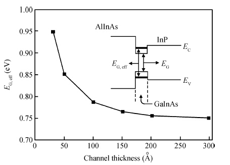
Fig. 1.
Effective energy-gap $E_{\rm G, eff}$ as a function of channel thickness. The inset shows the schematic energy-band diagram.
SEMICONDUCTOR DEVICES
Zhiming Wang1, , Xin Lü1, Xiaobin Luo1, Yuxing Cui2, Xiguo Sun2, Jianghui Mo2, Xingchang Fu2, Liang Li2 and Dawei He2
Corresponding author: Zhiming Wang, E-mail: wangzhiming872@163.com
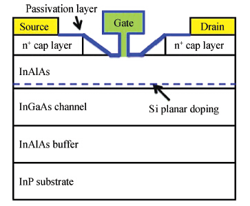
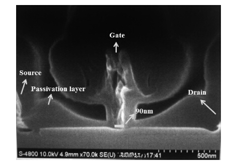
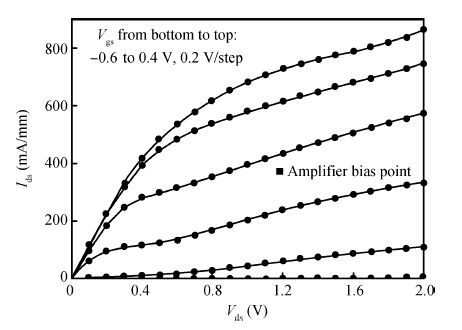
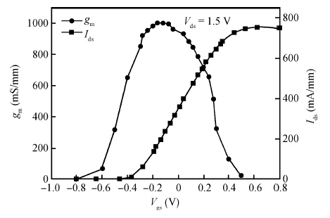
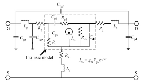
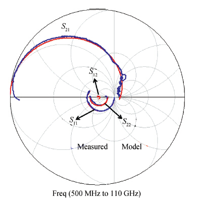
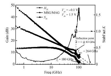
Abstract: 90-nm T-shaped gate InP-based In0.52Al0.48As/In0.6Ga0.4As pseudomorphic high electron mobility transistors were designed and fabricated with a gate-width of 2 × 30 μm, a source—drain space of 2.5 μm, and a source—gate space of 0.75 μm. DC, RF and small-signal model characterizations were demonstrated. The maximum saturation current density was measured to be 755 mA/mm biased at Vgs = 0.6 V and Vds = 1.5 V. The maximum extrinsic transconductance was measured to be 1006 mS/mm biased at Vgs = -0.1 V and Vds = 1.5 V. The extrapolated current gain cutoff frequency and maximum oscillation frequency based on S-parameters measured from 0.5 to 110 GHz were 180 and 264 GHz, respectively. The inflection point (the stability factor k= 1) where the slope from —10 dB/decade (MSG) to —20 dB/decade (MAG) was measured to be 83 GHz. The small-signal model of this device was also established, and the S-parameters of the model are consistent with those measured from 0.5—110 GHz.
Keywords: InP, PHEMTs, InAlAs/InGaAs, MMICs, small-signal modeling
| [1] | |
| [2] | |
| [3] | |
| [4] | |
| [5] | |
| [6] | |
| [7] | |
| [8] | |
| [9] | |
| [10] | |
| [11] | |
| [12] | |
| [13] | |
| [14] | |
| [15] |
| [1] | |
| [2] | |
| [3] | |
| [4] | |
| [5] | |
| [6] | |
| [7] | |
| [8] | |
| [9] | |
| [10] | |
| [11] | |
| [12] | |
| [13] | |
| [14] | |
| [15] |


Article views: 2941 Times PDF downloads: 26 Times Cited by: 0 Times
Received: 30 July 2014 Revised: Online: Published: 01 February 2015
| Citation: |
Zhiming Wang, Xin Lü, Xiaobin Luo, Yuxing Cui, Xiguo Sun, Jianghui Mo, Xingchang Fu, Liang Li, Dawei He. Design of InAlAs/InGaAs PHEMTs and small-signal modeling from 0.5 to 110 GHz[J]. Journal of Semiconductors, 2015, 36(2): 024005. doi: 10.1088/1674-4926/36/2/024005
****
Z M Wang, X Lü, X B Luo, Y X Cui, X G Sun, J H Mo, X C Fu, L Li, D W He. Design of InAlAs/InGaAs PHEMTs and small-signal modeling from 0.5 to 110 GHz[J]. J. Semicond., 2015, 36(2): 024005. doi: 10.1088/1674-4926/36/2/024005.

|
| [1] | |
| [2] | |
| [3] | |
| [4] | |
| [5] | |
| [6] | |
| [7] | |
| [8] | |
| [9] | |
| [10] | |
| [11] | |
| [12] | |
| [13] | |
| [14] | |
| [15] |

 WeChat ID
Journal of Semiconductors © 2017 All Rights Reserved 京ICP备05085259号-2

 DownLoad: