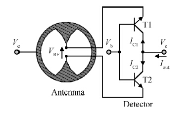
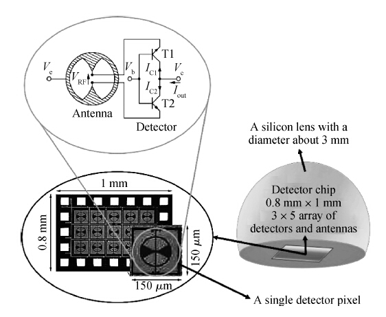
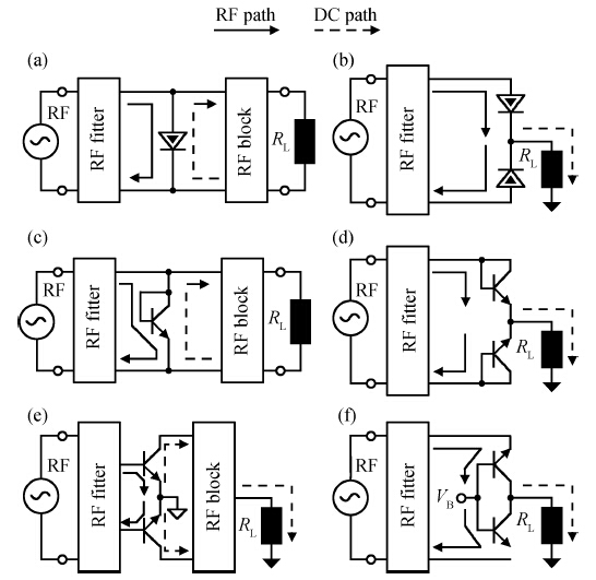
Loading [MathJax]/jax/output/HTML-CSS/jax.js
J. Semicond. > 2015, Volume 36 > Issue 5 > 054010

SEMICONDUCTOR DEVICES

Physical characteristics modification of a SiGe-HBT semiconductor device for performance improvement in a terahertz detecting system

Hamed Ghodsi and Hassan Kaatuzian

+ Author Affiliations

 Corresponding author: Hassan Kaatuzian, E-mail: hamed88@aut.ac.ir,hsnkato@aut.ac.ir

DOI: 10.1088/1674-4926/36/5/054010

PDF

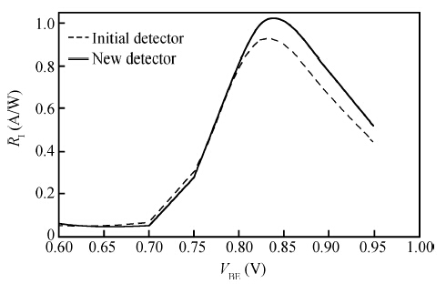
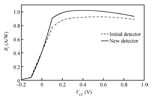
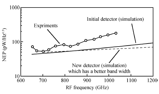
Abstract: In order to improve the performance of a pre-designed direct conversion terahertz detector which is implemented in a 0.25 μ m-SiGe-BiCMOS process, we propose some slight modifications in the bipolar section of the SiGe device physical design. Comparison of our new proposed device and the previously reported device is done by SILVACO TCAD software simulation and we have used previous experimentally reported data to confirm our software simulations. Our proposed modifications in device structural design show a present device responsivity improvement of about 10% from 1 to 1.1 A/W while the bandwidth improvement is about 218 GHz. The minimum noise equivalent power at detector output is increased by about 14.3% and finally power consumption per pixel at the maximum responsivity is decreased by about 5%.

Key words: terahertzSiGeHBTphysical structuredirect conversion detector

The Terahertz is a portion of the electromagnetic spectrum that lies between the optical and microwave regions. This has sometimes been called the "terahertz gap" because it lies between the frequencies where traditional electronics have a good performance and the optical frequencies that can be handled by optical devices. Terahertz electronic and optoelectronic devices have many important developing applications which can impact on our lives, for example in radio astronomy[1], medical imaging[1], security screening[1], terahertz spectroscopy and its applications[2], such as non-destructive testing (NDT) and biological industries[1].

Existing terahertz electronic detectors are mostly operated as coherent detectors made of Schottky diode mixers driven by a local oscillator (LO) and followed by an intermediate frequency (IF) filter. Despite the good performance of these types of detectors, this technology requires discrete waveguides and diodes, and thus have a big limitation in their commercial applications. Although coherent detectors can be integrated, for example in a SiGe-BiCMOS standard process[3], because of the local oscillator the power consumption of this type of detector is relatively high and thus these detectors are not suitable for implementation in large arrays. Large arrays are often needed in terahertz imaging systems for better resolution. However, the use of direct conversion detectors which are implemented without any local oscillator, with more integration facility, can provide good responsivity and noise characteristics with relatively lower power consumption than the coherent detectors. Moreover direct conversion detectors below the technology fT/fmax can be further improved, using LNAs. However, beyond the technology fT/fmax it is impossible to design LNAs. The solution is an antenna coupled with direct detectors, which are often based on the non-linearity of a diode (square-law) for the down conversion of a terahertz signal.

Continuing on from our previously published works, including References [9, 10, 11] where we described HBT devices based on III-V and SiGe compounds, in this research a direct conversion terahertz detector based on SiGe-HBT will be analyzed and some improvements will be proposed. The rest of this paper is structured as follows. Section 2 gives a brief introduction of detector design and how it works. Section 3 describes the device implementation and gives some details of our previous experimental setup. Section 4 puts forward our newly proposed design. In Section 5 the newly proposed device design and previous design will be compared and the better performance of the newly proposed detector, which has the benefit of using modified SiGe-HBT, will be shown. In Section 6 we will draw our conclusions.

Direct conversion detectors based on non-linear devices usually provide square-law rectification resulting in a DC component and a second harmonic RF signal. With an RF filter at the output RF signal, its second and higher harmonics are omitted and the output voltage or current is proportional to the RF input power. This is usually realized using a diode, such as that shown in Figure 1(a), which also has the required isolations between DC and RF signals to ensure that DC power leakage to the RF input and RF power leakage to DC output is avoided. A better topology with differential output that has the advantage of eliminating RF isolation by creating an AC ground at the output is shown in Figure 1(b).

Figure  1.  Some of possible square-law detector implementations[1].

In a bipolar technology, a single diode can be built with a transistor by connecting the collector and the base terminals, as presented in Figure 1(c), the differential topology of this detector is also shown in Figure 1(d). For a vertical device, where the collector is very large in comparison with the emitter, the performance of this detector will be reduced because the capacitive coupling to the substrate through the collector region reduces the RF power being injected into the device. A first solution to reduce the substrate coupling is to use a common-emitter circuit topology. In this case, RF isolation at the output would be required, as shown in Figure 1(e).

To better isolate the RF to substrate coupling, a differential common-base circuit can be used where the base and the collector are AC ground, as shown in Figure 1(f). This differential configuration, which we used in this paper, gives us the following advantages:

(1) An output DC ground where no RF isolation at the output is required. This makes the design easier to interface to conventional readout circuitry.

(2) An extra degree of freedom of the bias operating point, in comparison with the diode connected device. This extra freedom can be used for detector optimization.

(3) Isolation to the relatively large substrate.

(4) A CB configuration is better than CE in terms of frequency performance.

The implemented detector circuit as shown in Figure 2, and as mentioned before, is directly coupled to a differential antenna which is connected to the transistor emitters and the output DC current is proportional to the RF input, as explained in Equation (1).

IoutISA2RF4VT,(1)
where IS is reverse saturation current and VT is the thermal voltage.

Figure  2.  Differential THz detector schematic of a single pixel.

The implemented detector 3 × 5 array is shown in Figure 3, and each pixel output can be measured separately. A silicon lens which is 3 mm in diameter and 1.88 mm thick is constructed to converge the input THz wave into the chip with a Gaussian profile, where the maximum intensity is on the pixel which is at the center.

Figure  3.  Experimental setup for performance characterization of terahertz detector[1].

The implemented chip is constructed on a 150 μm thick die and the differential antenna, which has a diameter about 90~nm, is located on metal three at a distance of 8.75 μm from the silicon bulk within the five-layer silicon oxide BEOL (back-end-of-the-line) stack, which is 13.4 μm thick[1].

Responsivity and noise equivalent power are both important measures of a terahertz detector's performance. Optical responsivity is a measure of the electrical output strength per optical input power, either measured in current mode (RI) or voltage mode (RV). An accurate measurement of the optical responsivity requires an accurate measurement of the available optical input power (Pin) to the detector. To do so, a terahertz source with a measured total output power (PTX) and a specified antenna gain (GTX) is used to illuminate the detector placed at a distance (r), as shown in Figure 4. The available input power to the detector according to Friis transmission equation[6] is then given by:

Pin=PTXGTX4πr2Aeff,(2)
where Aeff=DRXλ2/(4π) and DRX is receiver antenna diversity. With the values shown in Figure 4 we can calculate the terahertz signal power at the detector input to be about 4.83~nW. We can now calculate the optical responsivity with Equation (3).

RI=IoutPin.

(3)
Figure  4.  Implemented detector details[1].

The noise equivalent power can be calculated from the ratio of the spot noise at the output in a specific modulation frequency$\footnote[1]{In order to facilitate the readout of the detector signal in the presence of a DC-offset and 1/f noise.}$ and output responsivity:

NEP=InRI.

(4)

Our previous detector implementation was done with a SiGe-HBT, which was developed by IHP MICROELECTRONICSTM, in a 0.25 μm SiGe-BiCMOS process. This device with a Beta of about 700 in VBE = 0.7 V and maximum fT/fmax = 280 GHz/435 GHz has a good performance if used in the detector circuit and as result the maximum responsivity and minimum NEP of the previous reported device is 1 A/W and 50 pW/Hz, respectively[1].

But we can apply the following modifications in order to have better performances:

(1) SiGe-base thickness decreased from 18 to 15 nm. With this change, base transit time and base internal field will be improved and as a result, device gain and frequency performance can both be improved. But the main reason for this change is to be more conservative about the SiGe base critical thickness.

(2) A SiC collector is implemented because it increases the unset of the base push out current[4] and thus improves device performance with a larger bandgap than the SiGe-base. This results in a barrier at the collector-base interface, which can effectively slow down the majority of electron carriers transmitting into the collector region[5]. The two common mechanisms of current flow through this barrier are thermionic emission and tunneling[7]. But thermionic emission has an inverse relation with the barrier height, which cannot be decreased, because we do not want to decrease the base internal field and current gain, which is exponentially related to the internal field. As a result we must increase the tunneling current through the barrier. The tunneling current is directly proportional to the slope of the conduction band in the collector region[8], which depends on the base-collector inverse bias and collector doping. Thus we should increase the collector doping level and also decrease the collector thickness in order to have a thinner depletion region and a sharper barrier, and thus higher tunneling current level. With some considerations about transistor break-down mechanisms, we prefer not to decease the collector thickness more than 30 nm (the initial value is 50 nm), 15 nm SiC, and 15 nm silicon, and thus the barrier width and its bad effects can be further decreased.

(3) Some other modifications in doping profiles also exist to optimize the device performance in both gain and frequency characteristics. However, these changes are small enough to be sure that the new device can still be implemented, and that the critical values for current density and electric field cannot downgrade the performance of the new device.

More details about the transistor's modifications and its new characteristics are mentioned in Table 1 and Figure 5.

Table  1.  Modified characteristics of new proposed transistor.
DownLoad: CSV  | Show Table
Figure  5.  The new proposed transistor.

First we should verify and confirm[5] our software simulator with the experimentally reported data[1]. Figures 6, 7, and 8 give the simulation results for the initial detector plotted with the experimental data, which can confirm our software simulator.

Figure  6.  Output DC current (VCE = 1 V) for a single pixel. The solid line is our simulation result and the squares are our experimental results[1].
Figure  7.  Responsivity for a single pixel of initial detector versus VBE with optimized VCE. The solid line is our simulation result and the squares are our experimental results[1].
Figure  8.  Responsivity for a single pixel of initial detector versus VCE with optimized VBE. The solid line is our simulation result and the squares are our experimental results[1].

The measurements that we used for comparison are responsivity, noise equivalent power, and bandwidth and power consumption. For example, responsivity versus VBE and VCE is plotted in Figures 9 and Figures 10, respectively, and noise equivalent power (NEP) versus RF frequency is plotted in Figure 11. Finally, in Table 2 we conclude important values, which show the better performance of the newly proposed device.

Figure  9.  Responsivity versus VBE when VCE is the value which has the maximum responsivity. A comparison between new detector and initial detector.
Figure  10.  Responsivity versus VCE when VBE is the value which has the maximum responsivity. A comparison between new detector and initial detector.
Figure  11.  NEP versus RF frequency when VBE and VCE are such that we have maximum responsivity. A comparison between new detector and initial detector. (Experimental data about initial detector are also added[1]).
Table  2.  Performance comparison table.
DownLoad: CSV  | Show Table

In this paper a pre-fabricated direct conversion terahertz detector has been analyzed and several modifications to the device's structural design (including doping level modifications, base and collector thickness decrement, and the addition of a silicon collector below the SiC collector region) have been applied.

By applying our proposed modifications, several improvements in the detector characteristics could be achieved including a responsivity improvement of about 10% and a bandwidth improvement of about 44%. As a result of increased current levels, the minimum noise equivalent power at detector output is increased to about 14.3% and, finally, the power consumption per pixel at the maximum responsivity is decreased by about 5%.

It should also be mentioned that the new device implementation will be more complex and some transistor performance limits, such as break down voltage, will be lowered. For the initial SiGe-HBT, BVCEO is about 1.7 V[1] and as mentioned for new SiGe-HBT this will be smaller. However, the trade-off between performance and these problems cannot be avoided and we should care about these difficulties.


[1]
[2]
[3]
[4]
[5]
[6]
[7]
[8]
[9]
[10]
[11]
Fig. 1.  Some of possible square-law detector implementations[1].

Fig. 2.  Differential THz detector schematic of a single pixel.

Fig. 3.  Experimental setup for performance characterization of terahertz detector[1].

Fig. 4.  Implemented detector details[1].

Fig. 5.  The new proposed transistor.

Fig. 6.  Output DC current (VCE = 1 V) for a single pixel. The solid line is our simulation result and the squares are our experimental results[1].

Fig. 7.  Responsivity for a single pixel of initial detector versus VBE with optimized VCE. The solid line is our simulation result and the squares are our experimental results[1].

Fig. 8.  Responsivity for a single pixel of initial detector versus VCE with optimized VBE. The solid line is our simulation result and the squares are our experimental results[1].

Fig. 9.  Responsivity versus VBE when VCE is the value which has the maximum responsivity. A comparison between new detector and initial detector.

Fig. 10.  Responsivity versus VCE when VBE is the value which has the maximum responsivity. A comparison between new detector and initial detector.

Fig. 11.  NEP versus RF frequency when VBE and VCE are such that we have maximum responsivity. A comparison between new detector and initial detector. (Experimental data about initial detector are also added[1]).

DownLoad: CSV
DownLoad: CSV

Table 1.   Modified characteristics of new proposed transistor.

DownLoad: CSV

Table 2.   Performance comparison table.

DownLoad: CSV
[1]
[2]
[3]
[4]
[5]
[6]
[7]
[8]
[9]
[10]
[11]
1

Performance analysis of SiGe double-gate N-MOSFET

A. Singh, D. Kapoor, R. Sharma

Journal of Semiconductors, 2017, 38(4): 044003. doi: 10.1088/1674-4926/38/4/044003

2

Dynamic threshold voltage operation in Si and SiGe source junctionless tunnel field effect transistor

Shibir Basak, Pranav Kumar Asthana, Yogesh Goswami, Bahniman Ghosh

Journal of Semiconductors, 2014, 35(11): 114001. doi: 10.1088/1674-4926/35/11/114001

3

Extraction of Temperature Parameters and Optimization of the Mextram 504 Model on SiGe HBT

Ren Zheng, Hu Shaojian, Jiang Bin, Wang Yong, Zhao Yuhang, et al.

Journal of Semiconductors, 2008, 29(5): 960-964.

4

A 2GHz Power Amplifier Realized in IBM SiGe BiCMOS Technology 5PAe

Song Jiayou, Wang Zhigong, Peng Yanjun

Journal of Semiconductors, 2008, 29(11): 2101-2105.

5

Growth of SiGe by D-UHV/CVD at Low Temperature

Zeng Yugang, Han Genquan, Yu Jinzhong

Journal of Semiconductors, 2008, 29(10): 1889-1892.

6

A Monolithic InGaP/GaAs HBT Power Amplifier Design with Improved Gain Flatness

Zhu Min, Yin Junjian, Zhang Haiying

Journal of Semiconductors, 2008, 29(8): 1441-1444.

7

Analysis and Optimization of Power Si1-x Gex/Si Heteroj unction Bipolar Transistor for Wireless Local Area Network Applications

Xue Chunlai, Shi Wenhua, Cheng Buwen, Yao Fei, Wang Qiming, et al.

Chinese Journal of Semiconductors , 2007, 28(S1): 435-438.

8

X Band MMIC Power Amplifier Based on InGaP/GaAs HBT

Chen Yanhu, Shen Huajun, Wang Xiantai, Ge Ji, Li Bin, et al.

Chinese Journal of Semiconductors , 2007, 28(5): 759-762.

9

Strain and Annealing Effect of SiGe/Si Heterostructure in Limited Area Grown by MBE

Yang Hongbin, Fan Yongliang, Zhang Xiangjiu

Chinese Journal of Semiconductors , 2007, 28(8): 1226-1231.

10

Multi-Finger Power SiGe HBT with Non-Uniform Finger Spacing

Jin Dongyue, Zhang Wanrong, Shen Pei, Xie Hongyun, Wang Yang, et al.

Chinese Journal of Semiconductors , 2007, 28(10): 1527-1531.

11

A Multi-Finger Si1-xGex/Si Heterojunction Bipolar Transistor for Wireless Power Amplifier Applications

Xue Chunlai, Shi Wenhua, Yao Fei, Cheng Buwen, Wang Hongjie, et al.

Chinese Journal of Semiconductors , 2007, 28(4): 496-499.

12

Characteristics of npn AlGaN/GaN HBT

Gong Xin, Ma Lin, Zhang Xiaoju, Zhang Jinfeng, Yang Yan, et al.

Chinese Journal of Semiconductors , 2006, 27(9): 1600-1603.

13

Design and Fabrication of Power Si1-xGex/Si Heterojunction Bipolar Transistor for Wireless Power Amplifier Applications

Xue Chunlai, Cheng Buwen, Yao Fei, Wang Qiming

Chinese Journal of Semiconductors , 2006, 27(1): 9-13.

14

Transport Current Model of SiGe HBT

Hu Huiyong, Zhang Heming, Dai Xianying, Xuan Rongxi, Cui Xiaoying, et al.

Chinese Journal of Semiconductors , 2006, 27(6): 1059-1063.

15

Effect of Si Intermediate Layer on High Relaxed SiGe Layer Grown Using Low Temperature Si Buffer

Yang Hongbin, Fan Yongliang

Chinese Journal of Semiconductors , 2006, 27(S1): 144-147.

16

Terahertz Semiconductor Quantum Well Devices

Liu H C, Luo H, Ban D, Wachter M, Song C Y, et al.

Chinese Journal of Semiconductors , 2006, 27(4): 627-634.

17

GaAs HBT Microwave Power Transistor with On-Chip Stabilization Network

Chen Yanhu, Shen Huajun, Wang Xiantai, Ge Ji, Li Bin, et al.

Chinese Journal of Semiconductors , 2006, 27(12): 2075-2079.

18

Two Kinds of Patterned SiGe Epitaxial Growth Technologies

Xu Yang, Wang Fei, Xu Jun, Liu Zhihong, Qian Peixin, et al.

Chinese Journal of Semiconductors , 2006, 27(S1): 389-391.

19

SiGe HBT Class AB Power Amplifier for Wireless Communications

JIA Hong-yong, LIU Zhi-nong, LI Gao-qing, QIAN Pei-xin

Chinese Journal of Semiconductors , 2002, 23(9): 921-924.

20

Carrier Depth Profile of Si/SiGe/Si n-p-n HBT Structural Materials Characterized by Electrochemical Capacitance- Voltage Method

Chinese Journal of Semiconductors , 2000, 21(11): 1050-1054.

1. Shur, M.. Si, SiGe, InP, III-N, and p-diamond FETs and HBTs for sub-terahertz and terahertz applications. Proceedings of SPIE - The International Society for Optical Engineering, 2020. doi:10.1117/12.2551204
2. Ghodsi, H., Kaatuzian, H. Analysis and design of a SiGe-HBT based terahertz detector for imaging arrays applications. Microelectronics Journal, 2019. doi:10.1016/j.mejo.2019.06.007
3. Jiang, J., Wang, Z., Chen, C. et al. Attenuation properties of millimeter wave atmospheric window propagation in plasma sheath. Qiangjiguang Yu Lizishu/High Power Laser and Particle Beams, 2016, 28(8): 083101. doi:10.11884/HPLPB201628.151073
  • Search

    Advanced Search >>

    GET CITATION

    Hamed Ghodsi, Hassan Kaatuzian. Physical characteristics modification of a SiGe-HBT semiconductor device for performance improvement in a terahertz detecting system[J]. Journal of Semiconductors, 2015, 36(5): 054010. doi: 10.1088/1674-4926/36/5/054010
    H Ghodsi, H Kaatuzian. Physical characteristics modification of a SiGe-HBT semiconductor device for performance improvement in a terahertz detecting system[J]. J. Semicond., 2015, 36(5): 054010. doi: 10.1088/1674-4926/36/5/054010.
    shu

    Export: BibTex EndNote

    Article Metrics

    Article views: 2647 Times PDF downloads: 19 Times Cited by: 3 Times

    History

    Received: 05 October 2014 Revised: Online: Published: 01 May 2015

    Catalog

      Email This Article

      User name:
      Email:*请输入正确邮箱
      Code:*验证码错误
      Hamed Ghodsi, Hassan Kaatuzian. Physical characteristics modification of a SiGe-HBT semiconductor device for performance improvement in a terahertz detecting system[J]. Journal of Semiconductors, 2015, 36(5): 054010. doi: 10.1088/1674-4926/36/5/054010 ****H Ghodsi, H Kaatuzian. Physical characteristics modification of a SiGe-HBT semiconductor device for performance improvement in a terahertz detecting system[J]. J. Semicond., 2015, 36(5): 054010. doi: 10.1088/1674-4926/36/5/054010.
      Citation:
      Hamed Ghodsi, Hassan Kaatuzian. Physical characteristics modification of a SiGe-HBT semiconductor device for performance improvement in a terahertz detecting system[J]. Journal of Semiconductors, 2015, 36(5): 054010. doi: 10.1088/1674-4926/36/5/054010 ****
      H Ghodsi, H Kaatuzian. Physical characteristics modification of a SiGe-HBT semiconductor device for performance improvement in a terahertz detecting system[J]. J. Semicond., 2015, 36(5): 054010. doi: 10.1088/1674-4926/36/5/054010.

      Physical characteristics modification of a SiGe-HBT semiconductor device for performance improvement in a terahertz detecting system

      DOI: 10.1088/1674-4926/36/5/054010
      More Information
      • Corresponding author: E-mail: hamed88@aut.ac.ir,hsnkato@aut.ac.ir
      • Received Date: 2014-10-05
      • Accepted Date: 2014-11-25
      • Published Date: 2015-01-25

      Catalog

        /

        DownLoad:  Full-Size Img  PowerPoint
        Return
        Return