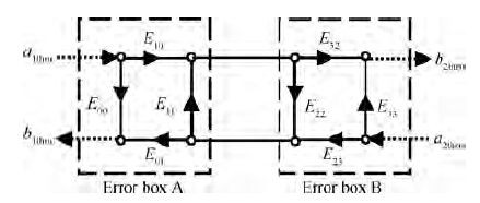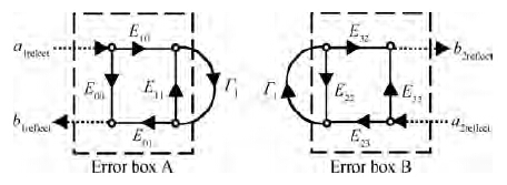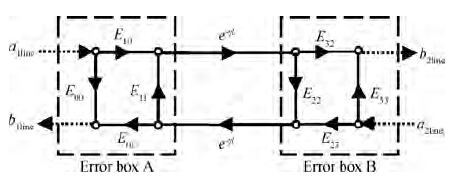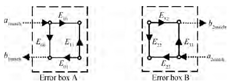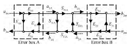
Fig. 1.
Eight-term error model.
SEMICONDUCTOR DEVICES
Guoping Tang1, Hongfei Yao2, Xiaohua Ma1, Zhi Jin2 and Xinyu Liu2,
Corresponding author: Xinyu Liu, E-mail: xyliu@ime.ac.cn
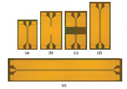
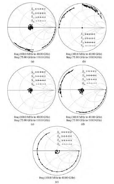
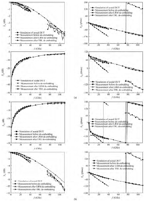
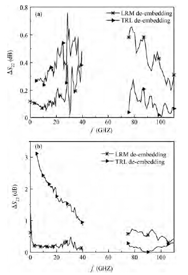
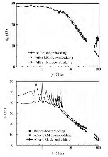
Abstract: On-wafer S-parameter de-embedding techniques from 0.1 to 110 GHz are researched. The solving results of thru-reflect-line (TRL) and line-reflect-match (LRM) de-embedding algorithms, when the input and output ports are asymmetric, are given. The de-embedding standards of TRL and LRM are designed on an InP substrate. The validity of the de-embedding results is demonstrated through two passive components, and the accuracy of TRL and LRM de-embedding techniques is compared from 0.1 to 110 GHz. By utilizing an LRM technique in 0.1-40 GHz and a TRL technique in 75-110 GHz, the intrinsic S-parameters of active device HBT in two frequency bands are obtained, and comparisons of the extracted small-signal current gain and the unilateral power gain before and after de-embedding are presented. The whole S-parameters of actual DUT from 0.1 to 110 GHz can be obtained by interpolation.
Keywords: model, millimeter-wave, de-embed, TRL, LRM
| [1] | |
| [2] | |
| [3] | |
| [4] | |
| [5] | |
| [6] | |
| [7] | |
| [8] | |
| [9] | |
| [10] | |
| [11] | |
| [12] | |
| [13] | |
| [14] | |
| [15] |

| [1] | |
| [2] | |
| [3] | |
| [4] | |
| [5] | |
| [6] | |
| [7] | |
| [8] | |
| [9] | |
| [10] | |
| [11] | |
| [12] | |
| [13] | |
| [14] | |
| [15] |


Article views: 5798 Times PDF downloads: 313 Times Cited by: 0 Times
Received: 06 August 2014 Revised: Online: Published: 01 May 2015
| Citation: |
Guoping Tang, Hongfei Yao, Xiaohua Ma, Zhi Jin, Xinyu Liu. On-wafer de-embedding techniques from 0.1 to 110 GHz[J]. Journal of Semiconductors, 2015, 36(5): 054012. doi: 10.1088/1674-4926/36/5/054012
****
G P Tang, H F Yao, X H Ma, Z Jin, X Y Liu. On-wafer de-embedding techniques from 0.1 to 110 GHz[J]. J. Semicond., 2015, 36(5): 054012. doi: 10.1088/1674-4926/36/5/054012.

|
| [1] | |
| [2] | |
| [3] | |
| [4] | |
| [5] | |
| [6] | |
| [7] | |
| [8] | |
| [9] | |
| [10] | |
| [11] | |
| [12] | |
| [13] | |
| [14] | |
| [15] |

 WeChat ID
Journal of Semiconductors © 2017 All Rights Reserved 京ICP备05085259号-2

 DownLoad: