J. Semicond. > 2015, Volume 36 > Issue 5 > 055011

SEMICONDUCTOR INTEGRATED CIRCUITS

A capacitive DAC with custom 3-D 1-fF MOM unit capacitors optimized for fast-settling routing in high speed SAR ADCs

Chixiao Chen, Jixuan Xiang, Huabin Chen, Jun Xu, Fan Ye, Ning Li and Junyan Ren

+ Author Affiliations

 Corresponding author: Junyan Ren, E-mail: jyren@fudan.edu.cn

DOI: 10.1088/1674-4926/36/5/055011

PDF

Abstract: 
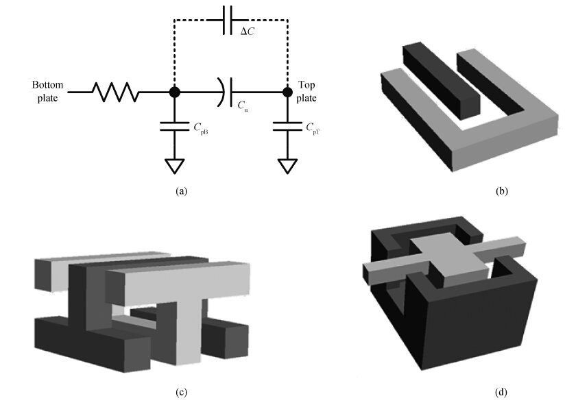
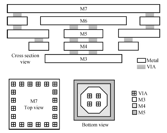
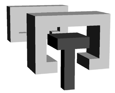
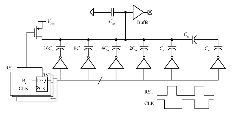
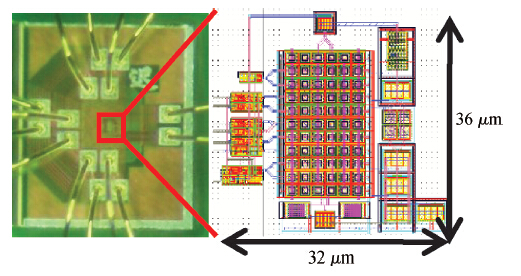
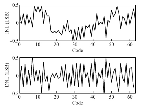
Asynchronous successive approximation register (SAR) analog-to-digital converters (ADC) feature high energy efficiency but medium performance. From the point of view of speed, the key bottleneck is the unit capacitor size. In this paper, a small size three-dimensional (3-D) metal-oxide-metal (MOM) capacitor is proposed. The unit capacitor has a capacitance of 1-fF. It shapes as an umbrella, which is designed for fast settling consideration. A comparison among the proposed capacitor with other 3-D MOM capacitors is also given in the paper. To demonstrate the effectiveness of the MOM capacitor, a 6-b capacitive DAC is implemented in TSMC 1P9M 65 nm LP CMOS technology. The DAC consumes a power dissipation of 0.16 mW at the rate of 100 MS/s, excluding a source-follower based output buffer. Static measurement result shows that INL is less than ± 1 LSB and DNL is less than ± 0.5 LSB. In addition, a 100 MS/s 9-bit SAR ADC with the proposed 3-D capacitor is simulated.

Key words: metal-oxide-metal capacitorSAR analog-to-digital convertorsdigital-to-analog convertors

As the CMOS process approaches tens of nanometers, such as 65 nm, 40 nm, and more advanced processes are being developed, the use of asynchronous successive approximation register (SAR) analog-to-digital convertors (ADC) are blooming due to their high energy efficiency. In contrast from synchronous SAR ADCs, asynchronous SAR ADCs have the same clock rate as the sampling rate. The internal beginning signal of each comparison step is generated by an ending signal of the last time comparison. Current state-of-the-art SAR ADCs are likely to have hundreds of mega-Hz sampling and medium resolution with FoMs of less than 100 fJ/conversion-step[1]. ADCs with these specification are likely to be implemented by flash and folding ADCs, which are much more power hungry than SAR ADCs.

However, there are several factors that prevent SAR ADCs from further accelerating to few Giga-Hz rate performance[2]. The first and foremost factor is the settling time issue. Inside a SAR ADC, the most time-demanding process is the most significant bit capacitor's (MSB) settling time. In other words, it is the time from the end the first comparison to the beginning of the second comparison. A conventional SAR ADC requires that the settling error of all comparisons should be less than 1/2~LSB, meaning that there is a long settling time for the MSB capacitor. Otherwise, there would be a missing code for certain analog inputs. Take the first order RC settling process as an example. The MSB settling time is known as,

tMSB>(N+1)RonCMSBln2,(1)
where N is the ADC's resolution bit, Ron and CMSB represents the time constant. For the rest bits, the settling time reduces exponentially due to the capacitor scaling. Therefore, tMSB is the most critical time determining the SAR ADC's speed. %From the point of view of implementation, the settling time is estimated by cascading several stages of the inverter-based delay line. Although some redundancy based architectures have been proposed[3], the simplest method to accelerate SAR ADCs is to minimize CMSB or the unit capacitor size.

Another issue related to the settling are the ripple effects of the reference voltage, especially for hundreds of Mega-Hz SAR ADCs, where traditional active reference buffers are likely to fail to drive the big capacitive load. The current solution is to utilize very large on-chip decoupling capacitors to filter the reference voltage ripples. The decoupling capacitors are positively proportional to the total capacitor size and unit capacitor size. %Unfortunately, this is area consuming. %Some other issues include the number of comparison step for a SAR ADC. Some methods like 2-b/step can relax the number and accelerate the ADC's rate[1].

Apparently, there is a straight forward way to accelerate the ADC's speed and avoid large area decoupling - minimizing the capacitor sizes so that they are as small as possible. A small size capacitor reduces the load of the settling process, as well as the driving requirement of the reference voltage. Moreover, smaller size capacitors can save more power dissipation. Note that the settling power consumption remains as,

Psettling=12αV2RefCload,(2)
where α is denoted as the switch frequency for the reference driver. However, foundries do not provide customized small capacitors that are suitable to SAR ADCs.

Traditionally, only metal-insulator-metal (MIM) capacitors are provided, which are area consuming and not suitable for application in SAR ADCs. MIM capacitors feature a high capacitance density and a strict DRC rule, resulting in a both power hungry and big-area capacitive tank. In contrast from MIM capacitors, MOM capacitors use the oxide between metals as a dielectric to build a capacitor. Customized 3-D MOM capacitors are now appearing that are suited to high speed SAR ADC design. In this paper, an umbrella-shaped 3-D MOM capacitor with around 1-fF capacitance is proposed. To verify its effectiveness, a capacitive DAC with the proposed capacitors is fabricated. %Simulation and measurement results meet the design expectation. %Section 2 will review other customized 3-D MOM capacitors, and Section 3 will introduce the proposed one. %The circuit implementation of the capacitive DAC would be detailed in Section 4. %Fabrication and experimental result would be demonstrated in Section 5, and section 6 concludes the paper.

To satisfy the operation of SAR ADCs, not only the capacitance but also the parasitics need to be counted. A general model of a MOM capacitor is given in Figure 1(a). In Figure 1(a), CpB and CpT stands for the parasitic on the bottom and top plate of the MOM capacitor. Cu is the unit capacitor that is expected. ΔC represents the extra coupling factor between bottom and top plate. This could be caused by the variation among capacitor tanks, but is more likely to be caused by the extra coupling between routing wire and one certain plate of the capacitor. This factor is of the most concern for MOM capacitors compared with MIM capacitors, especially from the view of layout.

Figure  1.  MOM capacitors for SAR ADCs. (a) A general model for unit MOM capacitor. (b-d) 3-D MOM capacitor from References [2, 4, 5], respectively.

From the aspect of precision, both ΔC and CpB would affect the linearity of the ADC. Assuming the cases without attenuating capacitor and that only MSB capacitor has these parasitics, the linearity issue is as follows,

Vin=VRefCuCM+CTotal(M1)+CpT[Do+SMΔCCu],(3)
where SM is bit decision of the MSB bit and Do is the overall digital output. Apparently, the SM×ΔC/Cu term causes discontinuity and nonlinearity between Vin and Do. Equation (3) can be easily derived into capacitors of other bits. Although CpB only affects in gain error in Equation (3), it would worsen the case when it comes to capacitive tanks with attenuating capacitors.

From the aspect of speed or settling time, the RC term in the bottom plate is the most critical issue. The lumped model in Figure 1(a) is too optimistic an approximation if the routing wire is too long. Cu also affects the settling. Note that both Cu and CpB term accumulate for MSBs by an order of 2N.

Several 3-D MOM capacitors have been proposed for high performance SAR ADCs, as shown in Figures 1(b), 1(c) and 1(d). The dark shadowed metal is the bottom plate, whereas the light shadowed metal is the top plate.

Figure 1(b) is an almost 2-D MOM capacitor with top plate contoured to the bottom plate[2]. The sidewall-like shape tends to share one side of wall with the next capacitor. The capacitor has a unit capacitance of 1.3 fF and parasitic of 0.7 fF. Note that this structure has a high value ΔC/Cu, which needs very careful layout work to maintain precision.

Figure 1(c) is a symmetric 3-D MOM capacitor[4]. In reality, the pattern was stacked and repeated in a multi-layer method. It also features a good matching nature over the peripheral effect. Its unit capacitance is 2.6 fF. The finger-based MOM capacitor provided by foundry's PDK is much like this topology, except that more layers are exploited. %However, the symmetric structure, in other words, CpB=CpT, makes no room for more optimization.

Figure 1(d) shows a 3-D MOM capacitor which has a pillared top plate enclosed by its bottom plate[5]. Considering it advanced technology, the unit capacitance is 0.78 fF with an area of 1 μm2. The motivation of the pillar-based is to have a very clear top-plate node; unfortunately, there is a penalty of a huge parasitic of the bottom plate. These parasitics may deteriorate the settling process.

Some other structures have also been proposed, like the sandwich-like structure in Reference {[3]}. But they cannot overweigh those mentioned in terms of performance.

In contrast from these previous custom capacitors, the proposed capacitor takes settling as a priority. In other words, it minimizes CpB as much as possible. Figure 2 shows the detail of the proposed 3-D MOM capacitor, including its cross section, top view, and bottom view. Generally speaking, the proposed MOM capacitor is a complementary version of that in Figure 1(d). It has a pillar based bottom plate, with edge expanding at the level of metal 6. The top plate is enclosed by the bottom plate in all directions. In this way, the distance between the bottom plate and top plate is minimized, as the DRC and DFM rule allows. Thus, the capacitive density is kept high, resulting in an area of 2×2 μm2 for 1 fF capacitance.

Figure  2.  Multi-view on the proposed 3-D MOM capacitor.

The capacitor starts from the third layer of metal (M3), because M1 and M2 have high amounts of parasitic with the silicon ploy and substrate. The edge expanding topology on M3 and M6 is to increase the coupling area between the two plates. Considering routing, M3 is chosen as an octagon to avoid asymmetry of the optical lithography. The routing layer of bottom plates is M3, and that of the top plate is M7. It is appreciated that routing M3 and M7 are perpendicular. To offer a more direct impression, a 3-D shape of the proposed MOM capacitor is illustrated in Figure 3. The back side is separated from the center part in the figure so as to reveal the inner structure. Also, the front side is neglected for the same reason.

Figure  3.  A 3-D illustration on the proposed custom MOM capacitor.

RC extraction EDA tools show all the capacitance, as demonstrated in Table~1, according to the general model in Figure 1(a). It is obvious that the proposed structure suffers a top plate parasitic issue. As the outer side of the MOM capacitor, the top plate may couple with nearby metals. For example, there is a closed dummy cell side wall, thus increasing CpT. However, CpT only causes a gain error and does not affect linearity, according to Equation (3).

According to Equation (3), the SAR ADC's resolution is limited by the ΔC/Cu factor. EDA tool extraction shows that ΔC/Cu is less than 0.3, or about 8-bit resolution. However, due to the big value of CpT, only a 2 bit capacitor is allowed to be implemented after an attenuating capacitor.

The proposed MOM capacitor features a very low extra coupling between the two plate and a minimal driving load for the bottom plate, though not fit for capacitive tanks with attenuating capacitors.

The low coupling characteristic overweighs the MOM capacitors in Figures 1(b) and 1(c). The main capacitance of the proposed capacitor is contributed by the enclosure structure. Routing wires far away from the pillar can be ignored for less than 8b resolution. Even for higher precision, it is easy to match the extra coupling with a careful layout job. On the other hand, the MOM capacitors in Figure 1(b) and 1(c) have complex routing coupling models. The minimal driving load characteristic overweighs the MOM capacitors in Figure 1(d). This is a key contribution for fast settling. Unlike the huge surface area of the bottom plate exposed to the overall environment in Figure 1(d), the proposed capacitor has a small volume bottom plate. As a result, the coupling of the bottom plate is also low. %Nevertheless, the surface area of the MOM capacitor in Fgure 1(d) is of immense size.

Table 1 also includes a quantitative comparison among capacitors based on the general electrical model given in Figure~1(a). These figures are slightly different from its original figures from their reference. To be fair, all of the capacitors are drawn under the same area (2×2 μm2) with the same process (TSMC CMOS 65 nm LP 1P9M process).

Table  1.  Comparison of the 3-D MOM Capacitors with same area and process.
DownLoad: CSV  | Show Table

One apparent drawback of the proposed capacitor is the high proportion of the top plate parasitic. The parasitic term is highly unfriendly for a capacitive tank with attenuating capacitors. Any top plate parasitic on the other node of the attenuating capacitor would cause a nonlinearity term,

VinVRefCuCTotal[MSBAtten.Bit2iDi+Atten.BitLSB(1CpONCTotal)2iDi],(4)
where CpON is the bad parasitic and the accumulative effect of the CpT in our capacitor model. A detailed analysis and expression can be seen in Reference {[6]}.

To verify the effectiveness of the capacitor, a capacitive DAC is implemented by 1P9M 65 nm LP CMOS technology. The circuit topology is shown in Figure 4.

Figure  4.  Circuit implementation of the test chip.

The test chip has a single-ended capacitive DAC architecture. To investigate the RC extraction EDA tools' effectiveness, the last bit is implemented by an attenuating capacitor. A source-follower based buffer is utilized to make the output track the charge conservation node. The RST and CLK signals are generated as a two-phase non-overlapping pattern. Periodical RST signal refreshes conservation node every cycle.

A Cfix capacitor is inserted at the conservation node. This additional capacitor is used to estimate the capacitance of the MOM device. The relationship between the LSB voltage step and Cfix follows,

VLSB=VrefCu2NCu+CpTtotal+CfixASF,(5)
where CpTtotal is the estimated value of the accumulative effect of the top plate parasitic, including the coupling among side-wall dummy cells. ASF is the gain of source follower buffer.

NMOS transistors are put under the capacitive tank, which is the most area-efficient way to decouple the reference voltage[2]. NMOS transistors are configured as MOS capacitors with high capacitance density but low linearity. Considering that the voltage source charges and discharges in a short instance, an inductive bonding wire may cause an additional reference problem for slow settling. Although on-chip regulation circuits work out for this problem, their power consumption may be several multiples of the ADC core. Another solution is to employ large decoupling capacitors as a charge reservoir to reduce the reference ripple. The NMOS capacitors play such roles in the design and give a large ratio between the high volume decoupling and the loading capacitor partially, about 1000 over 1.

The proposed MOM capacitor and the test bench capacitive DAC were fabricated by TSMC 65 nm CMOS Low power technology, under a power supply of 1.2 V. Figure 5 shows the layout die photo of the DAC. The capacitive tank covers the major area. The overall active devices cover an area of 36 × 32~μm2. At a conversion rate of 100 MHz, the power consumption of the DAC is 160 μW, excluding the source-follower based buffer. The buffer dissipates 480 μW to drive the on board load and test equipment.

Figure  5.  Die photo and detailed layout diagram.

Static measurements are implemented to reveal the post silicon linearity. The result is shown in Figure 6, where both INL and DNL are less than ±0.5 LSB for the 6-bit resolution. The average LSB step is 4.77 mV. When we substitute the voltage step into Equation (5), the Cu is very close to 1 fF, showing a good estimation by RC extraction EDA tools.

Figure  6.  Static measurement result including INL and DNL.

However, the periodical ripples occurring in the DNL waveform show the unpromising character of the actuating capacitor. Quantitative analysis suggests that the attenuating capacitor is over 50 greater than expected, which is not demonstrated by the EDA tools. This phenomenon meets the prediction given in Section 3.2, in that the proposed MOM capacitor does not have good performance when it comes to attenuating structure.

This paper proposes a 3-D MOM capacitor and its test bench circuit, a capacitive DAC. The proposed 3D MOM capacitor has a unit capacitance of 1-fF. The capacitor has a pillar based bottom plate, which is enclosed by a top plate like an umbrella. Compared with other custom capacitors, the capacitor features low extra decoupling and fast settling A 6-b capacitive DAC is implemented in TSMC 1P9M 65 nm LP CMOS technology under a power supply of 1.2 V. Due to the low capacitance, the DAC only consumes a power dissipation of 160~μW at a rate of 100 MS/s. Static measurements are performed, demonstrating that both INL and DNL are less than ±0.5 LSB, even with one bit attenuating structure.


[1]
[2]
[3]
[4]
[5]
[6]
Fig. 1.  MOM capacitors for SAR ADCs. (a) A general model for unit MOM capacitor. (b-d) 3-D MOM capacitor from References [2, 4, 5], respectively.

Fig. 2.  Multi-view on the proposed 3-D MOM capacitor.

Fig. 3.  A 3-D illustration on the proposed custom MOM capacitor.

Fig. 4.  Circuit implementation of the test chip.

Fig. 5.  Die photo and detailed layout diagram.

Fig. 6.  Static measurement result including INL and DNL.

DownLoad: CSV
DownLoad: CSV
DownLoad: CSV

Table 1.   Comparison of the 3-D MOM Capacitors with same area and process.

DownLoad: CSV
DownLoad: CSV
DownLoad: CSV
[1]
[2]
[3]
[4]
[5]
[6]
1

Analytical model for the effects of the variation of ferrolectric material parameters on the minimum subthreshold swing in negative capacitance capacitor

Raheela Rasool, Najeeb-ud-Din, G. M. Rather

Journal of Semiconductors, 2019, 40(12): 122401. doi: 10.1088/1674-4926/40/12/122401

2

Subthreshold analog techniques

Nanjian Wu

Journal of Semiconductors, 2019, 40(2): 020204. doi: 10.1088/1674-4926/40/2/020204

3

Dual material gate doping-less tunnel FET with hetero gate dielectric for enhancement of analog/RF performance

Sunny Anand, R.K. Sarin

Journal of Semiconductors, 2017, 38(2): 024001. doi: 10.1088/1674-4926/38/2/024001

4

A multi-channel analog IC for in vitro neural recording

Feng Yuan, Zhigong Wang, Xiaoying Lü

Journal of Semiconductors, 2016, 37(2): 025007. doi: 10.1088/1674-4926/37/2/025007

5

Synthesis of metal oxide composite nanosheets and their pressure sensing properties

Muhammad Tariq Saeed Chani, Sher Bahadar Khan, Kh. S. Karimov, M. Abid, Abdullah M. Asiri, et al.

Journal of Semiconductors, 2015, 36(2): 023002. doi: 10.1088/1674-4926/36/2/023002

6

High quality metal-quantum dot-metal structure fabricated with a highly compatible self-aligned process

Yingchun Fu, Xiaofeng Wang, Liuhong Ma, Yaling Zhou, Xiang Yang, et al.

Journal of Semiconductors, 2015, 36(12): 123004. doi: 10.1088/1674-4926/36/12/123004

7

The impact of gate misalignment on the analog performance of a dual-material double gate junctionless transistor

S. Intekhab Amin, R. K. Sarin

Journal of Semiconductors, 2015, 36(9): 094001. doi: 10.1088/1674-4926/36/9/094001

8

VCCS controlled LDO with small on-chip capacitor

Qiuli Li, Yao Qian, Danzhu Lü, Zhiliang Hong

Journal of Semiconductors, 2014, 35(11): 115011. doi: 10.1088/1674-4926/35/11/115011

9

A 750 MHz semi-digital clock and data recovery circuit with 10-12

Wei Xueming, Wang Yiweng, Li Ping, Luo Heping

Journal of Semiconductors, 2011, 32(12): 125009. doi: 10.1088/1674-4926/32/12/125009

10

A low-power and low-phase-noise LC digitally controlled oscillator featuring a novel capacitor bank

Tian Huanhuan, Li Zhiqiang, Chen Pufeng, Wu Rufei, Zhang Haiying, et al.

Journal of Semiconductors, 2010, 31(12): 125003. doi: 10.1088/1674-4926/31/12/125003

11

A high-performance, low-power ΣΔ ADC for digital audio applications

Luo Hao, Han Yan, Ray C. C. Cheung, Han Xiaoxia, Ma Shaoyu, et al.

Journal of Semiconductors, 2010, 31(5): 055009. doi: 10.1088/1674-4926/31/5/055009

12

A low power 3.125 Gbps CMOS analog equalizer for serial links

Ju Hao, Zhou Yumei, Jiao Yishu

Journal of Semiconductors, 2010, 31(11): 115003. doi: 10.1088/1674-4926/31/11/115003

13

Comparison of electron transmittances and tunneling currents in an anisotropic TiNx/HfO2/SiO2/p-Si(100) metal–oxide–semiconductor (MOS) capacitor calculated using exponential- and Airy-wavefunction app

Fatimah A. Noor, Mikrajuddin Abdullah, Sukirno, Khairurrijal

Journal of Semiconductors, 2010, 31(12): 124002. doi: 10.1088/1674-4926/31/12/124002

14

A 12 bit 100 MS/s pipelined analog to digital converter without calibration

Cai Xiaobo, Li Fule, Zhang Chun, Wang Zhihua

Journal of Semiconductors, 2010, 31(11): 115007. doi: 10.1088/1674-4926/31/11/115007

15

Design of an ultra-low-power digital processor for passive UHF RFID tags

Shi Wanggen, Zhuang Yiqi, Li Xiaoming, Wang Xianghua, Jin Zhao, et al.

Journal of Semiconductors, 2009, 30(4): 045004. doi: 10.1088/1674-4926/30/4/045004

16

TDDB improvement by optimized processes on metal–insulator–silicon capacitors with atomic layer deposition of Al2O3 and multi layers of TiN film structure

Peng Kun, Wang Biao, Xiao Deyuan, Qiu Shengfen, Lin D C, et al.

Journal of Semiconductors, 2009, 30(8): 082005. doi: 10.1088/1674-4926/30/8/082005

17

Digital Coarse Tuning Loop for Wide-Band Fast-Settling Dual-Loop Frequency Synthesizers

Liu Junhua, Liao Huailin, Yin Jun, Huang Ru, Zhang Xing, et al.

Chinese Journal of Semiconductors , 2006, 27(11): 1911-1917.

18

Design and Analysis of Analog Front-End of Passive RFID Transponders

Hu Jianyun, He Yan, Min Hao

Chinese Journal of Semiconductors , 2006, 27(6): 999-1005.

19

A Novel Sampling Switch Suitable for Low-Voltage Analog-to-Digital Converters

Peng Yunfeng, Zhou Feng

Chinese Journal of Semiconductors , 2006, 27(8): 1367-1372.

20

Noise Analysis of Analog Correlator

Tu Chunjiang, Liu Bo’an,and Chen Hongyi

Chinese Journal of Semiconductors , 2005, 26(3): 480-486.

1. Chandak, V.S., Kumbhar, M.B., Kulal, P.M. Structural, optical and magnetic studies of Cr-doped ZnO nanoparticles prepared by co-precipitation method. Inorganic Chemistry Communications, 2025. doi:10.1016/j.inoche.2024.113766
2. Devi, L.R., Esakki, E.S., Sundar, S.M. Synthesis, characterization and properties of Cr-doped ZnO nanoparticles via a facile solvothermal route. International Journal of Modern Physics B, 2025, 39(2): 2550015. doi:10.1142/S0217979225500158
3. Zhang, Z., Ren, Y., Li, X. Ferromagnetic behavior of Cr-doped ZnS nanosheets prepared by solvothermal method. Phase Transitions, 2025. doi:10.1080/01411594.2024.2448260
4. Rizwana Begum, S., Anitha, A.G., Thirumurugan, A. et al. Insights into the compositional and temperature-mediated magnetic characteristics of chromium-doped ZnO nanoparticles. Journal of Physics Condensed Matter, 2024, 36(38): 385805. doi:10.1088/1361-648X/ad581e
5. Kummara, S.K., Reddy, L. Tailored Optical, Magnetic and Photoluminescence properties of Fe/Cr-doped ZnO nanoparticles synthesized via solution combustion method. Nano-Structures and Nano-Objects, 2024. doi:10.1016/j.nanoso.2024.101263
6. Petrov, D.N., Dang, N.T., Co, N.D. et al. Enhanced photocatalytic activity and ferromagnetic ordering in hydrogenated Zn1−xCoxO. Journal of Materials Science, 2024, 59(21): 9217-9236. doi:10.1007/s10853-024-09724-z
7. Jangannanavar, V.D., Basavanagoudra, H., Patil, M.K. et al. Nanocrystal engineering: Unraveling bioactivities and augmented photocatalytic degradation of ZnO and Cr-doped ZnO via green and chemical synthesis routes. Journal of Molecular Structure, 2024. doi:10.1016/j.molstruc.2023.137340
8. Salem, M., Ghannam, H., Boussaid, A. et al. Surface Passivation of Crystalline Silicon Solar Cells by Cr:ZnO Coating Layers. Silicon, 2024, 16(6): 2465-2471. doi:10.1007/s12633-024-02852-w
9. Lokesha, H.S., Prinsloo, A.R.E., Mohanty, P. et al. Impact of Cr doping on the structure, optical and magnetic properties of nanocrystalline ZnO particles. Journal of Alloys and Compounds, 2023. doi:10.1016/j.jallcom.2023.170815
10. Garcés, L., Garcia, C.R., Oliva, J. et al. Novel strategies for the enhancement of the NIR emission in the Ca doped ZnO system: Doping with Cr or adding Sb2S3. Optical Materials, 2023. doi:10.1016/j.optmat.2023.114302
11. Muktaridha, O., Adlim, M., Suhendrayatna, S. et al. Progress of 3d metal-doped zinc oxide nanoparticles and the photocatalytic properties. Arabian Journal of Chemistry, 2021, 14(6): 103175. doi:10.1016/j.arabjc.2021.103175
12. Munir, T., Mahmood, A., Ahmad, N. et al. Structural, electrical and optical properties of Zn1−xCuxO (x = 0.00–0.09) nanoparticles. Journal of King Saud University - Science, 2021, 33(2): 101330. doi:10.1016/j.jksus.2020.101330
13. Kiruthiga, A., Kannan, R., Krishnakumar, T. Investigation of structural and optical characteristics of chromium doped ZnO nanostructures by microwave irradiated route for sensing applications. AIP Conference Proceedings, 2020. doi:10.1063/5.0019393
14. Amami, P.E., Das, J., Mishra, D.K. et al. Cr doped ZnO: Investigation of magnetic behaviour through SQUID and ESR studies. Physica B: Condensed Matter, 2019. doi:10.1016/j.physb.2019.07.056
15. Debnath, T., Bandyopadhyay, A., Chakraborty, T. et al. Influence of different Cr concentrations on the structural and ferromagnetic properties of ZnO nanomaterials prepared by the hydrothermal synthesis route. Materials Research Bulletin, 2019. doi:10.1016/j.materresbull.2019.05.005
16. Singh, P., Kumar, R., Singh, R.K. Progress on Transition Metal-Doped ZnO Nanoparticles and Its Application. Industrial and Engineering Chemistry Research, 2019, 58(37): 17130-17163. doi:10.1021/acs.iecr.9b01561
17. Mahmood, Q., Ul Haq, B., Yaseen, M. et al. Exploring the origin of p-type half-metallic ferromagnetism in beryllium doped alkali based perovskites. Solid State Communications, 2019. doi:10.1016/j.ssc.2019.113654
18. Malaidurai, M., Santosh Kumar, B., Thangavel, R. Spin polarized carrier injection driven magneto-optical Kerr effect in Cr-doped ZnO nanorods. Physics Letters, Section A: General, Atomic and Solid State Physics, 2019, 383(24): 2988-2992. doi:10.1016/j.physleta.2019.06.031
19. Nguyen, S.N., Truong, T.K., You, S.-J. et al. Investigation on Photocatalytic Removal of NO under Visible Light over Cr-Doped ZnO Nanoparticles. ACS Omega, 2019, 4(7): 12853-12859. doi:10.1021/acsomega.9b01628
20. Akshay, V.R., Arun, B., Mandal, G. et al. Visible range optical absorption, Urbach energy estimation and paramagnetic response in Cr-doped TiO2 nanocrystals derived by a sol-gel method. Physical Chemistry Chemical Physics, 2019, 21(24): 12991-13004. doi:10.1039/c9cp01351b
  • Search

    Advanced Search >>

    GET CITATION

    Khizar-ul Haq, M. Irfan, Muhammad Masood, Murtaza Saleem, Tahir Iqbal, Ishaq Ahmad, M. A. Khan, M. Zaffar, Muhammad Irfan. Enhanced room temperature ferromagnetism in Cr-doped ZnO nanoparticles prepared by auto-combustion method[J]. Journal of Semiconductors, 2018, 39(4): 043001. doi: 10.1088/1674-4926/39/4/043001
    K Haq, M Irfan, M Masood, M Saleem, T Iqbal, I Ahmad, M A Khan, M Zaffar, M Irfan. Enhanced room temperature ferromagnetism in Cr-doped ZnO nanoparticles prepared by auto-combustion method[J]. J. Semicond., 2018, 39(4): 043001. doi: 10.1088/1674-4926/39/4/043001.
    shu

    Export: BibTex EndNote

    Article Metrics

    Article views: 3840 Times PDF downloads: 146 Times Cited by: 20 Times

    History

    Received: 09 September 2014 Revised: Online: Published: 01 May 2015

    Catalog

      Email This Article

      User name:
      Email:*请输入正确邮箱
      Code:*验证码错误
      Chixiao Chen, Jixuan Xiang, Huabin Chen, Jun Xu, Fan Ye, Ning Li, Junyan Ren. A capacitive DAC with custom 3-D 1-fF MOM unit capacitors optimized for fast-settling routing in high speed SAR ADCs[J]. Journal of Semiconductors, 2015, 36(5): 055011. doi: 10.1088/1674-4926/36/5/055011 ****C X Chen, J X Xiang, H B Chen, J Xu, F Ye, N Li, J Y Ren. A capacitive DAC with custom 3-D 1-fF MOM unit capacitors optimized for fast-settling routing in high speed SAR ADCs[J]. J. Semicond., 2015, 36(5): 055011. doi: 10.1088/1674-4926/36/5/055011.
      Citation:
      Chixiao Chen, Jixuan Xiang, Huabin Chen, Jun Xu, Fan Ye, Ning Li, Junyan Ren. A capacitive DAC with custom 3-D 1-fF MOM unit capacitors optimized for fast-settling routing in high speed SAR ADCs[J]. Journal of Semiconductors, 2015, 36(5): 055011. doi: 10.1088/1674-4926/36/5/055011 ****
      C X Chen, J X Xiang, H B Chen, J Xu, F Ye, N Li, J Y Ren. A capacitive DAC with custom 3-D 1-fF MOM unit capacitors optimized for fast-settling routing in high speed SAR ADCs[J]. J. Semicond., 2015, 36(5): 055011. doi: 10.1088/1674-4926/36/5/055011.

      A capacitive DAC with custom 3-D 1-fF MOM unit capacitors optimized for fast-settling routing in high speed SAR ADCs

      DOI: 10.1088/1674-4926/36/5/055011
      More Information
      • Corresponding author: E-mail: jyren@fudan.edu.cn
      • Received Date: 2014-09-09
      • Accepted Date: 2014-10-23
      • Published Date: 2015-01-25

      Catalog

        /

        DownLoad:  Full-Size Img  PowerPoint
        Return
        Return