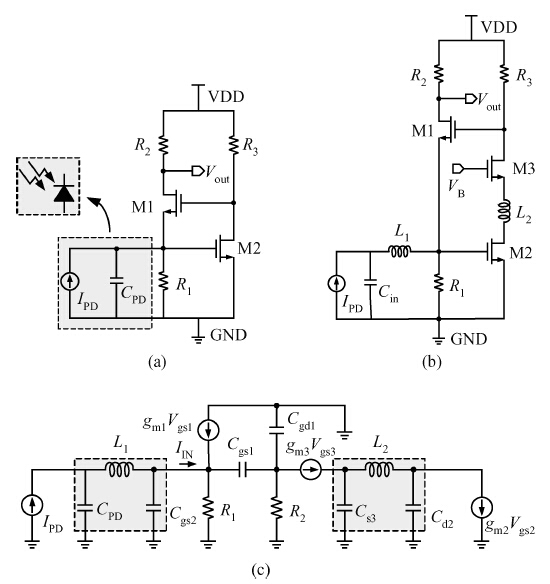
Fig. 1.
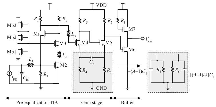
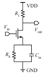
(a) Conventional RGC circuit. (b) Modified pre-equalization RGC circuit. (c) Small-signal model of the pre-equalization modified RGC circuit.
SEMICONDUCTOR INTEGRATED CIRCUITS
Qiwei Song1, Luhong Mao1, , Sheng Xie1 and Yuzhuo Kang2
Corresponding author: Luhong Mao, E-mail: lhmao@tju.edu.cn
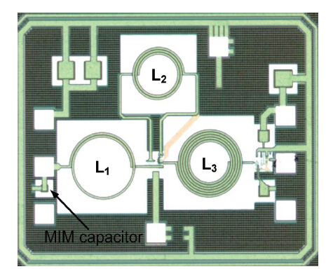
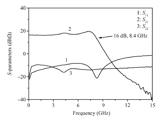
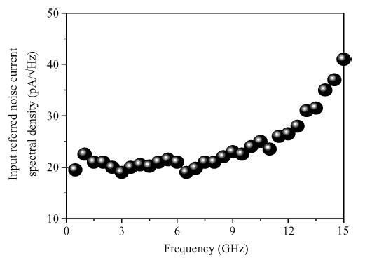
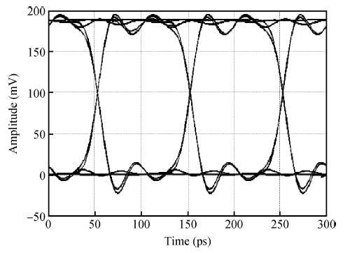
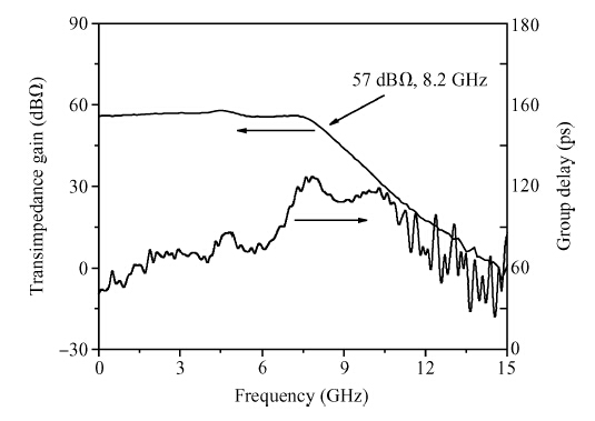
Abstract: This paper presents a modified regulated cascode (RGC) transimpedance amplifier (TIA) with a novel pre-equalized technique. The pre-equalized circuit employed the broadband series inductive π-network and Gm-boosting technique. The introduction of this technique compensates the transferred signal at the input port of the TIA without an increase in power dissipation. Furthermore, a novel miller capacitance degeneration method is designed in the gain stage for further bandwidth improvement. The TIA is realized in UMC 0.18 μm CMOS technology and tested with an on-chip 0.3 pF capacitor to emulate a photodetector (PD). The measured transimpedance gain amounts to 57 dBΩ with a -3 dB bandwidth of about 8.2 GHz and consumes only 22 mW power from a single 1.8 V supply.
Keywords: pre-equalized, Gm-boosting, series inductive π-network, miller capacitance degeneration
| [1] | |
| [2] | |
| [3] | |
| [4] | |
| [5] | |
| [6] | |
| [7] | |
| [8] | |
| [9] | |
| [10] | |
| [11] | |
| [12] | |
| [13] | |
| [14] |
| [1] | |
| [2] | |
| [3] | |
| [4] | |
| [5] | |
| [6] | |
| [7] | |
| [8] | |
| [9] | |
| [10] | |
| [11] | |
| [12] | |
| [13] | |
| [14] |


Article views: 3336 Times PDF downloads: 53 Times Cited by: 0 Times
Received: 29 December 2014 Revised: Online: Published: 01 July 2015
| Citation: |
Qiwei Song, Luhong Mao, Sheng Xie, Yuzhuo Kang. Novel pre-equalization transimpedance amplifier for 10 Gb/s optical interconnects[J]. Journal of Semiconductors, 2015, 36(7): 075002. doi: 10.1088/1674-4926/36/7/075002
****
Q W Song, L H Mao, S Xie, Y Z Kang. Novel pre-equalization transimpedance amplifier for 10 Gb/s optical interconnects[J]. J. Semicond., 2015, 36(7): 075002. doi: 10.1088/1674-4926/36/7/075002.

|
| [1] | |
| [2] | |
| [3] | |
| [4] | |
| [5] | |
| [6] | |
| [7] | |
| [8] | |
| [9] | |
| [10] | |
| [11] | |
| [12] | |
| [13] | |
| [14] |

 WeChat ID
Journal of Semiconductors © 2017 All Rights Reserved 京ICP备05085259号-2

 DownLoad: