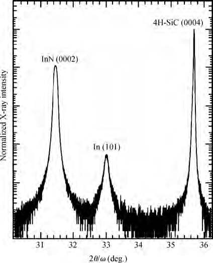
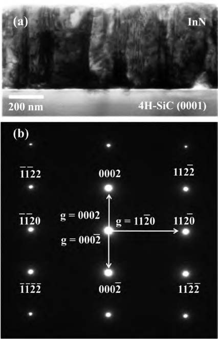
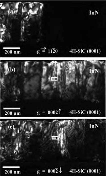
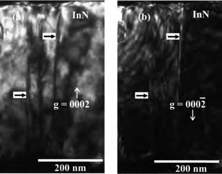
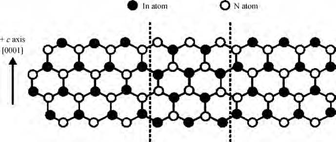
Abstract: InN film was grown on 4H-SiC (0001) substrate by RF plasma-assisted molecular beam epitaxy (RF-MBE). Prior to the growth of InN film, an InN buffer layer with a thickness of ~ 5.5 nm was grown on the substrate. Surface morphology, microstructure and structural quality of InN film were investigated. Micro-structural defects, such as stacking faults and anti-phase domain in InN film were carefully investigated using transmission electron microscopy (TEM). The results show that a high density of line contrasts, parallel to the growth direction (c-axis), was clearly observed in the grown InN film. Dark field TEM images recorded with diffraction vectors g = 11$\overline{2}$0 and g = 0002 revealed that such line contrasts evolved from a coalescence of the adjacent misoriented islands during the initial stage of the InN nucleation on the substrate surface. This InN nucleation also led to a generation of anti-phase domains.
Keywords:
RF-MBE, TEM, InN, threading dislocation, anti-phase domain, crystal polarity


 DownLoad: