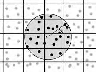
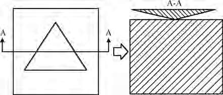
Processing math: 100%
J. Semicond. > 2015, Volume 36 > Issue 8 > 083007

SEMICONDUCTOR MATERIALS

Nano-indentation study on the (001) face of KDP crystal based on SPH method

Xiaoguang Guo, Ziyuan Liu, Hang Gao and Dongming Guo

+ Author Affiliations

 Corresponding author: Ziyuan Liu, Email: lzy5307827@126.com

DOI: 10.1088/1674-4926/36/8/083007

PDF

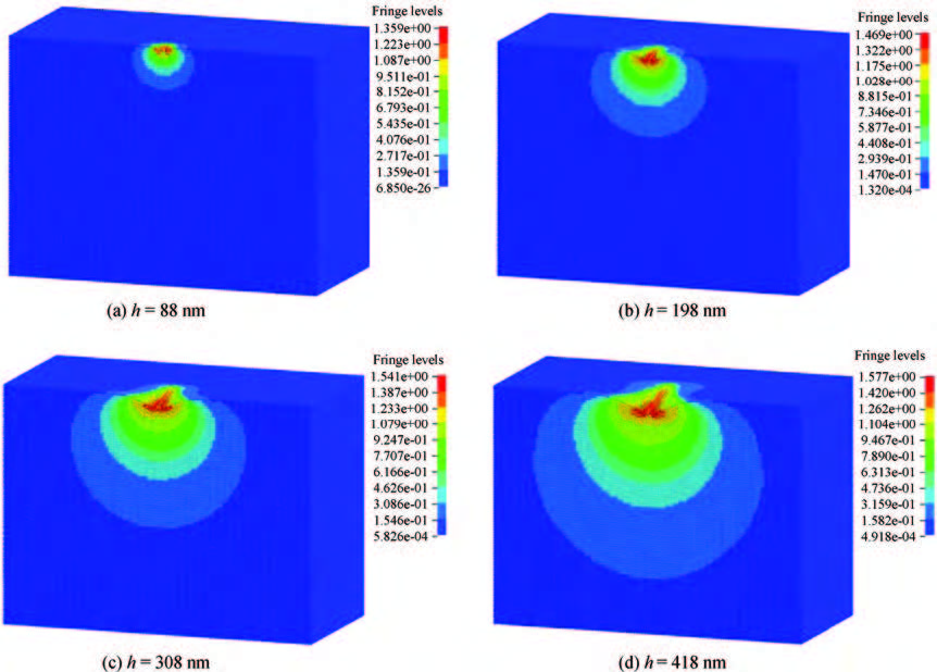
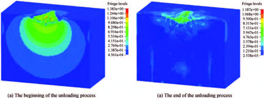
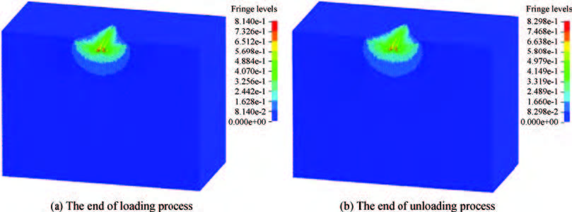
Abstract: In order to avoid the defects of mesh distortion when dealing with large deformation problems through using the finite element method, a mess-free simulation method——smooth particle hydrodynamics (SPH) has been introduced. The material constitutive model of KDP crystal has been established based on the elastic-plastic theory. Then the nano-indentation on the (001) face of KDP crystal has been carried out using SPH method. Simulation results show that the maximum equivalent stress and the maximum plastic strain concentrate on the area that located near the tip of the indenter during the loading process. The distribution shape of Von Mises stress is similar to concentric circles. During the unloading process, no obvious variation of plastic strain distribution exists. The maximum Von Mises stress is mainly located at the indentation and its edge at the end of the unloading process. The approximate direct proportion relationship between the maximum indentation depth and the depth of the maximum Von Mises stress distribution has been discovered when the maximum load is lower than 8 mN. In addition, the nano-indentation experiments on KDP crystal's (001) face have been carried out. Both the material parameters and the adjusted stress-strain curve have been verified. The hindering role of the affected layer has been found and analyzed.

Key words: KDP crystal(001) facenano-indentationSPHnumerical simulation

Potassium dihydrogen phosphate crystal (KDP) is an important nonlinear optical material which has been used widely in the fields of electro-optical modulation,photoelectric switches and nonlinear optics for frequency conversion[1, 2]. Because of KDP crystal's special material properties (e.g.,soft texture,high brittleness,easy deliquescence,sensitivity to temperature change and strong anisotropy),it has become one of the most difficult machining materials worldwide[3]. Moreover,extremely high surface quality must be guaranteed for the inertial confinement fusion (ICF) which is the most valuable application of KDP crystal[4, 5]. However,damage that is mainly due to plastic deformation and fracture behaviors is unavoidable in the process of surface machining. In order to fully understand the mechanism of damage generation,it is necessary to make profound research into the nano mechanics behaviors of KDP crystal[6].

The mechanical properties of KDP crystal have been previously studied using conventional micro-indentation and nano-indentation. Sengupta et al.[7] have found the indentation size effect during nano-indentation experiments on the (001) face of KDP crystal. The Knoops indentation experiments for the (001) and (100) faces of KDP crystal have been studied by Tong et al.[8]. Both the breaking tenacity and the approximation model of the tetragonal system have been obtained. Kucheyev et al.[9] have analyzed the pop-in phenomenon. They have also concluded that the nature of KDP crystal's plastic deformation is slippage. Based on the elastic constants of materials,Lu\linebreak et al.[10] have studied the size effect phenomena of elastic modulus and nano-hardness. Guo et al.[11] have recently studied the adhesion effect during the unloading process. However,indentation tests which are expensive and time-consuming seem not enough to fully discover the mechanical properties of KDP crystal. Fortunately,numerical simulation provides an innovation method to solve these problems[12,\,13]. Nevertheless,the finite element method (FEM) which has been used widely in the field of numerical simulation has some fatal drawbacks. One of them is mesh distortion when dealing with large deformation problems. To solve these issues,a mesh-free simulation method (i.e.,smooth particle hydrodynamics,SPH) has been introduced.

In this paper,both the elastic-plastic behavior and the potential fracture mechanics behavior on the (001) face of KDP crystal have been analyzed using the SPH method. In addition,nano-indentation experiments have been carried out to verify the rationality of the simulation.

The SPH method is a mess-free,Lagrangian type numerical simulation method which was first proposed by Lucy,Gingold and Monaghan[14]. This method was initially used for simulations of astrophysical phenomena. Then it has been widely used in fluid mechanics and continuous solid mechanics[15]. It has the ability to solve large deformation problems,not only because of the self-adaptive approximation method,but also because the formula structure of SPH is not influenced by the randomness of particle distribution[16]. Compared with the traditional FEM in these aspects,the SPH method is unparalleled.

The basis of the SPH method is the interpolation theory. Any macroscopic variables (e.g.,density,temperature and pressure) can be calculated through integral interpolation of a set of disordered particles.

The SPH method is used for solving the energy and the velocity of a number of points at any time. All of these points have certain mass. They are called “particles”. The approximate function which describes the motion information of particles during a period of time is expressed as Equation (1).

hf(x)=f(y)W(xy,h)dy,

(1)

where W is the kernel function (interpolation kernel),which is expressed as Equation (2).

W(x,h)=1hd(x)θ(x),

(2)

where h is the smoothing length,which changes with time and space. d is the space dimension. W(x,h) is the rush function,as is shown in Figure 1.

Figure  1.  Kernel function.

The smooth kernel which is most commonly used in the SPH method is the cubic B-spline. It is defined as Equation (3).

θ(u)=C×{11.5u2+0.75u3,|u|1,0.25(2u3),1|u|2,0,|u|>2,

(3)

where C is normalization constant,and is determined by space dimension[17].

The neighbor search is an important step in SPH computation. Which particles will interact with each other must be known at any time during the calculation process. The range of influence for each particle is a spherical area with a radius of 2h (Figure 2). The aim of the neighbor search is to list all the particles belonging to this area during each time step. The “bucket” contact searching algorithm which can save lots of time is applied well at present. The basic principle of the algorithm is dividing the whole area into several sub areas first. Then for each particle,not only the neighbors inside the main box,but also the neighbor boxes contained in the domain of influence of the given particle is searched (Figure 2)[18].

Figure  2.  Bucket sorting and neighbor searchŒ [18].

Smoothing length is mainly used to guarantee that there are enough neighbors during the compression and the expansion of the material so that the approximation of continuous variable particle is still effective. Both the maximum value and the minimum value need to be set up because of the numerical reasons. It is expressed as Equation (4).

HMINh0hHMAXh0,

(4)

where h0 is the initial smoothing length. HMIN and HMAX are the scale factors.

The Berkovich indenter that is made of diamond is introduced. The sketch of Berkovich indenter is shown in Figure 3. Considering the elastic modulus of diamond is far greater than KDP crystal,the indenter has been set as a rigid body. The relevant material parameters of diamond are given in Table 1.

Figure  3.  The sketch of Berkovich indenter.
Table  1.  Relevant material parameters of diamond.
DownLoad: CSV  | Show Table

To make an adaptive description for the KDP crystal,a 3D SPH particle model is introduced (Figure 4). The Saint-Venant's principle says: if the forces acting on a small portion of the surface of an elastic body are replaced by another statically equivalent system of forces acting on the same portion of the surface,this redistribution of loading produces substantial changes in the stresses locally but has a negligible effect on the stresses at distances which are large in comparison with the linear dimensions of the surface on which the forces are changed[19]. With the consideration of both the Saint-Venant's principle and the computation time,the dimension of the rectangular workpiece is set as 8 × 8 × 6 μm3.

Figure  4.  3D modeling of KDP crystal’s nano-indentation.

At present,the material model which can make a full description of both soft brittle and anisotropy properties in LS-DYNA doesn't exist. The interaction between the workpiece and the indenter happens at microscopic level. In the case of little influence on the result of the simulation,KDP crystal has been simplified as the homogeneous isotropic material which is independent of the strain rate. So the multi-linear elastic-plastic model has been introduced to describe the elasto-plastic mechanical properties of KDP crystal's (001) face. Some relevant material parameters of KDP crystal are given in Table 2. In this paper,KDP crystal's plastic properties can be obtained through amending other materials which have similar material properties. The adjusted stress-strain curve is shown in Figure 5.

Table  2.  Relevant material parameters of KDP crystal’s (001) face.
DownLoad: CSV  | Show Table
Figure  5.  The adjusted stress-strain curve.

For the bottom of the work piece,all degrees of freedom are constrained in order to represent the supporting plane. The boundary conditions of SPH particles differ from the finite elements. The way we choose is to define a symmetry plane by creating a set of ghost particles. For each particle close to the boundary,a ghost particle is automatically created by reflecting the particle itself. The ghost particle has the same mass,pressure,and absolute velocity as the real particle. It is in the list of neighbors of that particle so as to affect the process of particle approximation.

Considering that the Von Mises stresses under different maximum load conditions are similar in the nanoindentation process,8 mN maximum load is set as a typical sample to analyze the variation of Von Mises stress at first. The section view is selected because the relative position between the indenter and the work piece leads to some difficulties for observation (Figure 6). The indenter is also hidden so as to make the outcome clearer.

Figure  6.  The section view of nano-indentation.

The distribution area of Von Mises stress which is located right below the indenter is small at the beginning of the interaction between indenter and KDP crystal (Figure 7(a)). Simultaneously,a certain extent of stress concentration can be seen near the indenter's tip. Elastic deformation is the main deformation style at this period. As the indentation depth increases,the Von Mises stress not only expands to the bottom of the work piece,but also expands to both sides of the indenter (Figure 7(b)). The stress concentration becomes more obvious. Based on the fracture mechanics theory,a crack will arise right below the tip of the indenter when the stress which lies in the stress concentration area reaches beyond the cracking toughness of KDP crystal[20]. Although the maximum load cannot reach beyond the cracking toughness during the nano-indentation tests,the trend of crack formation and expansion can be truly inferred from the simulation outcomes. In addition,a large scale of the yield effect appears in this period. The form of deformation of KDP crystal changes from elastic to plastic. When the indenter goes deeper,the distribution area of Von Mises stress becomes larger. Meanwhile,the stress concentration area has a distribution like the circular arc appear on both sides of the indenter (Figure 7(d)). Moreover,this stress distribution tends to expand. The tests show that this stress distribution area is the main reason for the formation of radial cracks[21]. Simulation results provide a theoretical support for the indentation fracture tests.

Figure  7.  (Color online) The distribution of Von Mises stress during the loading process.

As is shown in Figure 8(a),the maximum Von Mises stress is not located exactly right below the indenter,and there is a certain distance between them at the beginning of the unloading process. The main reason is that the elastic recovery behavior was hindered by the plastic deformation which arises during the loading process. The Von Mises stress that exists in the form of the residual stress is mainly located at the indentation and its edge at the end of the unloading process (Figure 8(b)). Part of the residual stress can be released from the expansion of damage and defects. However no damage and defects exist in the process of simulation. This factor leads to the phenomenon that the theoretical value of residual stress is always larger than that of experiments.

Figure  8.  (Color online) The distribution of Von Mises stress during the unloading process.

In addition,a series of the nano-indentaion simulations of KDP crystal's (001) face under different maximum loads (i.e.,1,2,4,6,8 mN) have been studied. The variable “k” is the ratio of the maximum indentation depth (m) and the influence depth of the maximum Von Mises stress (n) corresponding to the maximum load (Table 3). With the increase of the maximum indentation depth,the influence depth of the maximum Von Mises stress increases as well. The ratio of the two is almost constant. So the maximum indentation depth is approximately proportional to the influence depth of the maximum Von Mises stress. Actually,some inherent defect areas where the yield strength and the breaking tenacity are lower than normal are unavoidable within KDP crystal. When the stress has an impact on these defect areas,damage expansion is most likely to occur. So in the machining process of KDP crystal,the cutting depth must be small in order to avoid the damage expansion as far as possible.

Table  3.  m, n and k under different maximum load.
DownLoad: CSV  | Show Table

The indentation process under 8 mN maximum load is set as a typical sample to analyze the plastic strain. As is shown in Figure 9(a),the majority of plastic strain is located right below the indenter. The distribution of plastic strain is very similar to that of Von Mises stress which has been mentioned above. Since the contact depth between KDP crystal and the indention's tip is always the largest contrasting other contact areas,the stress belonging to this area in which the plastic deformation is larger than the others reaches the yield strength first. Contrasting Figures 9(a) and 9(b),nearly no variation of plastic strain distribution exists during the unloading process. This can be explained by the plastic deformation theory. When the stress has not reached beyond the yield limit during the loading process,the atomic arrangement of KDP crystal keeps to the original state. In the meantime,the deformation of KDP crystal can recover. Conversely,when the stress reaches beyond the yield limit,the atomic arrangement changed forever in the plastic deformation area. As the Neumann principle says: the macroscopic physical properties of crystals necessarily reflect the crystals' microstructure and the change of micro-structure will lead to the variation of macroscopic mechanical properties[2]. This is exactly the generation mechanism of the affected layer during the machining process of KDP crystal.

Figure  9.  (Color online) The distribution of plastic strain under 8 mN maximum load.

The (001) face of KDP crystal samples were made by the diamond wire saw slicing. The dimension of these samples is 10 × 10 × 5 mm3. Then through the lapping process and the ultra-precision polishing process,the quality of these samples meets the basic requirements of nanoindentaion experiments. Only the best surface quality sample where surface roughness is 1.556 nm (Ra) was chosen for further research in order to reduce the influence of surface quality on the experimental outcome as much as possible.

The TriboIndenter nano-indentation test system was used (Figure 10) at room temperature. The load resolution of this system is 3 nN. The maximum load is 12.6 mN. The Berkovich indenter that is made of diamond was introduced. The shape of the indenter is triangular pyramid in which the angle between the seamed edge and the central line is 77.05,and the angle between the side and the central line is 65.3. The indentation system was carefully calibrated by indenting fused silica with known material properties. An 8 mN maximum load was set for the nano-indentation experiment at the beginning. The load increment was set as 100 μN/s. The comparison of the pressure-indentation depth curve between the experiment and the SPH simulation is shown in Figure 11.

Figure  10.  The appearance of TriboIndenter.
Figure  11.  The pressure-indentation depth curve under 8 mN.

As is shown in Figure 11,the simulation curve roughly coincides with the experimental one. The correlation coefficient has been introduced in order to test the degree of correspondence between the experimental curve and the simulation one. Its value is 0.999015648 which has proven that the degree of similarity of the two curves is relatively high. Both the material properties of KDP crystal's (001) face and the revised stress-strain curve have been verified. The yield stress is 120 MPa.

The nano-indentation experiments of KDP crystal's (001) face using different maximum loads (i.e.,1,2,4,6,8 mN) have also been carried out under the same experiment conditions. The comparison of the maximum indentation depth between the experiments and the simulations is shown in Figure 12.

Figure  12.  The comparison of the maximum indentation depth.

As is shown in Figure 12,the maximum indentation depth of the experiments is smaller than that of the simulations when the maximum loads are 1,2,4,6 mN respectively. The reason is the inevitable influence of the affected layer which is the production of the scratch that occurs between the abrasive and KDP crystal during the polishing process. The affected layer is mainly made up of dislocation,plastic deformation and residual stress[22]. So the material hardness of the affected layer is bigger than usual. The interaction between the indenter and the KDP crystal is mainly located at the affected layer under relatively small load. The movement of the indenter is hindered by dislocation,plastic deformation and residual stress,whereas no affected layer exists during the simulation and the hindering effect does not exist. This is why the maximum indentation depths of the experiments are smaller than that of the simulations when the maximum loads are relatively small. However,the simulation depth and the experiment depth are almost equal under 8 mN maximum load. The reason for this is that the impact of the deep areas where the material properties of KDP crystal are normal is becoming more and more obvious as the load continues to increase.

(1) The SPH method has been successfully introduced to simulate the nano-indentation on the (001) face of KDP crystal instead of FEM which has a mesh distortion defect when dealing with large deformation problems.

(2) The material constitutive model of KDP crystal which is available for the SPH method has been established based on the elastic-plastic theory.

(3) Both the distribution of Von Mises stress and the changing rule of the plastic strain have been obtained. The maximum Von Mises stress and plastic strain concentrate on the area that located near the tip of indenter. No obvious variation of plastic strain exists during the unloading process. The maximum Von Mises is mainly located at the indentation and its edge at the end of unloading.

(4) The approximate direct proportion relationship between the maximum indentation depth and the influence depth of the maximum Von Mises stress has been observed through nano-indentation simulations under different maximum load.

(5) The nano-indentation experiments on KDP crystal's (001) face have been carried out based on the simulation results. Both the material parameters and the adjusted stress-strain curve have been verified. The yield stress of KDP crystal is 120 MPa.

(6) The maximum indentation depth of the experiments is smaller than that of the simulations under low maximum load due to the hindering role of the affected layer.


[1]
[2]
[3]
[4]
[5]
[6]
[7]
[8]
[9]
[10]
[11]
[12]
[13]
[14]
[15]
[16]
[17]
[18]
[19]
[20]
[21]
[22]
Fig. 1.  Kernel function.

Fig. 2.  Bucket sorting and neighbor searchŒ [18].

Fig. 3.  The sketch of Berkovich indenter.

Fig. 4.  3D modeling of KDP crystal’s nano-indentation.

Fig. 5.  The adjusted stress-strain curve.

Fig. 6.  The section view of nano-indentation.

Fig. 7.  (Color online) The distribution of Von Mises stress during the loading process.

Fig. 8.  (Color online) The distribution of Von Mises stress during the unloading process.

Fig. 9.  (Color online) The distribution of plastic strain under 8 mN maximum load.

Fig. 10.  The appearance of TriboIndenter.

Fig. 11.  The pressure-indentation depth curve under 8 mN.

Fig. 12.  The comparison of the maximum indentation depth.

Table 1.   Relevant material parameters of diamond.

DownLoad: CSV

Table 2.   Relevant material parameters of KDP crystal’s (001) face.

DownLoad: CSV

Table 3.   m, n and k under different maximum load.

DownLoad: CSV
[1]
[2]
[3]
[4]
[5]
[6]
[7]
[8]
[9]
[10]
[11]
[12]
[13]
[14]
[15]
[16]
[17]
[18]
[19]
[20]
[21]
[22]
1

A crystal graph multilayer descriptor

Dahai Wei

Journal of Semiconductors, 2020, 41(8): 080202. doi: 10.1088/1674-4926/41/8/080202

2

Numerical study of mono-crystalline silicon solar cells with passivated emitter and rear contact configuration for the efficiency beyond 24% based on mass production technology

Peng Wang, Gaofei Li, Miao Wang, Hong Li, Jing Zheng, et al.

Journal of Semiconductors, 2020, 41(6): 062701. doi: 10.1088/1674-4926/41/6/062701

3

Simulation and application of external quantum efficiency of solar cells based on spectroscopy

Guanlin Chen, Can Han, Lingling Yan, Yuelong Li, Ying Zhao, et al.

Journal of Semiconductors, 2019, 40(12): 122701. doi: 10.1088/1674-4926/40/12/122701

4

Steady-state solution growth of microcrystalline silicon on nanocrystalline seed layers on glass

R. Bansen, C. Ehlers, Th. Teubner, T. Boeck

Journal of Semiconductors, 2016, 37(9): 093001. doi: 10.1088/1674-4926/37/9/093001

5

Numerical simulation of the effect of gold doping on the resistance to neutron irradiation of silicon diodes

K. Bekhouche, N. Sengouga, B. K. Jones

Journal of Semiconductors, 2015, 36(1): 014001. doi: 10.1088/1674-4926/36/1/014001

6

Analytical modeling and simulation of germanium single gate silicon on insulator TFET

T. S. Arun Samuel, N. B. Balamurugan

Journal of Semiconductors, 2014, 35(3): 034002. doi: 10.1088/1674-4926/35/3/034002

7

Optimization of the emitter region and the metal grid of a concentrator silicon solar cell

Yupeng Xing, Peide Han, Yujie Fan, Shuai Wang, Peng Liang, et al.

Journal of Semiconductors, 2013, 34(5): 054005. doi: 10.1088/1674-4926/34/5/054005

8

Modeling and simulation of centroid and inversion charge density in cylindrical surrounding gate MOSFETs including quantum effects

P. Vimala, N. B. Balamurugan

Journal of Semiconductors, 2013, 34(11): 114001. doi: 10.1088/1674-4926/34/11/114001

9

Nanoindentation on the doubler plane of KDP single crystal

Xiaoguang Guo, Xiaoji Zhang, Xianzhao Tang, Dongming Guo, Hang Gao, et al.

Journal of Semiconductors, 2013, 34(3): 034001. doi: 10.1088/1674-4926/34/3/034001

10

H-plasma-assisted aluminum induced crystallization of amorphous silicon

Li Juan, Liu Ning, Luo Chong, Meng Zhiguo, Xiong Shaozhen, et al.

Journal of Semiconductors, 2012, 33(6): 066003. doi: 10.1088/1674-4926/33/6/066003

11

Growth of CdS crystals by the physical vapor transport method

Cheng Hongjuan, Xu Yongkuan, Yang Wei, Yu Xianglu, Yan Ruyue, et al.

Journal of Semiconductors, 2009, 30(10): 103002. doi: 10.1088/1674-4926/30/10/103002

12

A novel GAAC FinFET transistor: device analysis, 3D TCAD simulation, and fabrication

Xiao Deyuan, Wang Xi, Yuan Haijiang, Yu Yuehui, Xie Zhifeng, et al.

Journal of Semiconductors, 2009, 30(1): 014001. doi: 10.1088/1674-4926/30/1/014001

13

Optical properties in 1D photonic crystal structure using Si/C60 multilayers

Chen Jing, Tang Jiyu, Han Peide, Chen Junfang

Journal of Semiconductors, 2009, 30(4): 043001. doi: 10.1088/1674-4926/30/4/043001

14

Wall Temperature Simulation of a Radial Flow MOCVD Reactor with Three-Separate Vertical Inlets

Nie Yuhong, Liu Yong, Yao Shouguang

Chinese Journal of Semiconductors , 2007, 28(1): 127-130.

15

Numerical Explanation of Slow Transients in an AlGaN/GaN HEMT

Zhang Jinfeng, Hao Yue

Chinese Journal of Semiconductors , 2006, 27(2): 276-282.

16

Energy Transfer Probability Between Host and Guest in Doped Organic Electrophosphorescent Devices

Li Hongjian, Ouyang Jun, Dai Guozhang, Dai Xiaoyu, Pan Yanzhi, et al.

Chinese Journal of Semiconductors , 2006, 27(4): 674-678.

17

Photolithography Process Simulation for Integrated Circuitsand Microelectromechanical System Fabrication

Zhou Zaifa, Huang Qing'an, Li Weihua

Chinese Journal of Semiconductors , 2006, 27(4): 705-711.

18

Fabrication and Numerical Simulation of a Micromachined Contact Cantilever RF-MEMS Switch

Sun Jianhai, Cui Dafu, Xiao Jiang

Chinese Journal of Semiconductors , 2006, 27(2): 309-312.

19

Two-Dimensional Static Numerical Modeling and Simulation of AlGaN/GaN HEMT

Xue Lijun, Xia Yang, Liu Ming, Wang Yan, Shao Xue, et al.

Chinese Journal of Semiconductors , 2006, 27(2): 298-303.

20

Simulation of a Monolithic Integrated CMOS Preamplifier for Neural Recordings

Sui Xiaohong, Liu Jinbin, Gu Ming, Pei Weihua, Chen Hongda, et al.

Chinese Journal of Semiconductors , 2005, 26(12): 2275-2280.

1. Shen, H., Brousseau, E., Kulasegaram, S. Assessment and validation of SPH modeling for nano-indentation. Computational Particle Mechanics, 2022. doi:10.1007/s40571-022-00514-5
2. Chen, S., Zhang, W. Study on the effect of titanium implant technology combined with nano indentation on the vertical control of pass. Acta Medica Mediterranea, 2021, 37(4): 2465-2470. doi:10.19193/0393-6384_2021_4_384
3. Gouskov, A., Nikolaev, S., Kuts, V. et al. Analysis of displacement fields of particle shaping surface during nanoscale ductile mode cutting of brittle materials. International Journal of Advanced Manufacturing Technology, 2018, 95(5-8): 1911-1918. doi:10.1007/s00170-017-1233-x
  • Search

    Advanced Search >>

    GET CITATION

    Xiaoguang Guo, Ziyuan Liu, Hang Gao, Dongming Guo. Nano-indentation study on the (001) face of KDP crystal based on SPH method[J]. Journal of Semiconductors, 2015, 36(8): 083007. doi: 10.1088/1674-4926/36/8/083007
    X G Guo, Z Y Liu, H Gao, D M Guo. Nano-indentation study on the (001) face of KDP crystal based on SPH method[J]. J. Semicond., 2015, 36(8): 083007. doi: 10.1088/1674-4926/36/8/083007.
    shu

    Export: BibTex EndNote

    Article Metrics

    Article views: 2629 Times PDF downloads: 18 Times Cited by: 3 Times

    History

    Received: 27 December 2014 Revised: Online: Published: 01 August 2015

    Catalog

      Email This Article

      User name:
      Email:*请输入正确邮箱
      Code:*验证码错误
      Xiaoguang Guo, Ziyuan Liu, Hang Gao, Dongming Guo. Nano-indentation study on the (001) face of KDP crystal based on SPH method[J]. Journal of Semiconductors, 2015, 36(8): 083007. doi: 10.1088/1674-4926/36/8/083007 ****X G Guo, Z Y Liu, H Gao, D M Guo. Nano-indentation study on the (001) face of KDP crystal based on SPH method[J]. J. Semicond., 2015, 36(8): 083007. doi: 10.1088/1674-4926/36/8/083007.
      Citation:
      Xiaoguang Guo, Ziyuan Liu, Hang Gao, Dongming Guo. Nano-indentation study on the (001) face of KDP crystal based on SPH method[J]. Journal of Semiconductors, 2015, 36(8): 083007. doi: 10.1088/1674-4926/36/8/083007 ****
      X G Guo, Z Y Liu, H Gao, D M Guo. Nano-indentation study on the (001) face of KDP crystal based on SPH method[J]. J. Semicond., 2015, 36(8): 083007. doi: 10.1088/1674-4926/36/8/083007.

      Nano-indentation study on the (001) face of KDP crystal based on SPH method

      DOI: 10.1088/1674-4926/36/8/083007
      Funds:

      Project supported by the National Basic Research Program of China (No. 51135002), and the Science Fund for Creative Research Groups (No. 51321004).

      More Information
      • Corresponding author: Email: lzy5307827@126.com
      • Received Date: 2014-12-27
      • Accepted Date: 2015-03-16
      • Published Date: 2015-01-25

      Catalog

        /

        DownLoad:  Full-Size Img  PowerPoint
        Return
        Return