


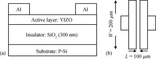
Fig. 1.
(a) Cross section and (b) electrode structure of YIZO TFT.
SEMICONDUCTOR MATERIALS
Dandan Wang, Qingpu Wang, Hanbin Wang, Xijian Zhang, Liwei Wu, Fujie Li and Shuai Yuan
Corresponding author: Wang Qingpu, wangqingpu@sdu.edu.cn
Abstract: Yttrium-doped IZO (YIZO) thin films with different thickness have been prepared on soda-lime glass (SLG) and P-Si substrates by radio frequency magnetron sputtering at room temperature. Structural morphology and optical properties of the films have been investigated. YIZO thin film transistors (TFTs) with the bottom-gate-structure are fabricated on P-Si substrates. The output and transfer characteristics of YIZO-TFT have been studied. It has been found that all YIZO thin films prepared at room temperature are amorphous, and the YIZO TFTs exhibit n-channel depletion mode. YIZO-TFT with active layer thickness of 20 nm shows an on/off ratio over 105, a sub-threshold swing of 2.20 V/decade at a low operating voltage of -1.0 V, and saturation mobility values over 0.57 cm2/(V· s).
Keywords: Y doped IZO, thin film, TFT, active layer
| [1] | |
| [2] | |
| [3] | |
| [4] | |
| [5] | |
| [6] | |
| [7] | |
| [8] | |
| [9] | |
| [10] | |
| [11] | |
| [12] | |
| [13] | |
| [14] | |
| [15] | |
| [16] | |
| [17] | |
| [18] | |
| [19] | |
| [20] | |
| [21] | |
| [22] | |
| [23] | |
| [24] | |
| [25] | |
| [26] |
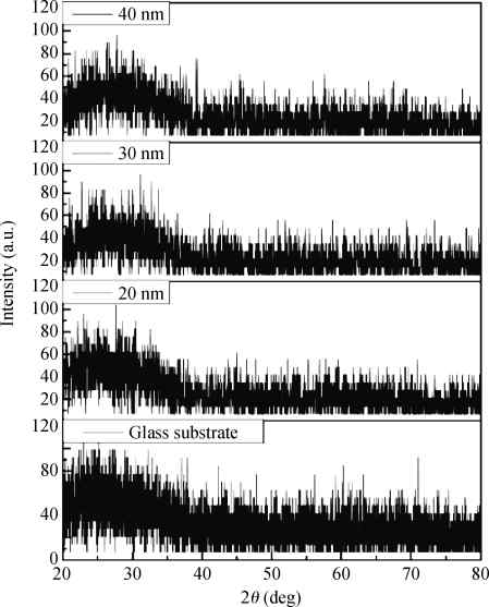
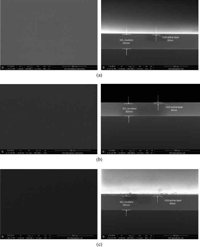
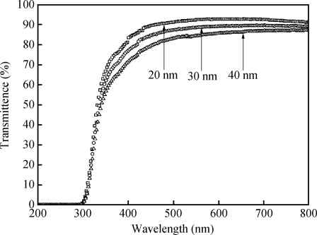
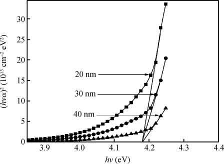
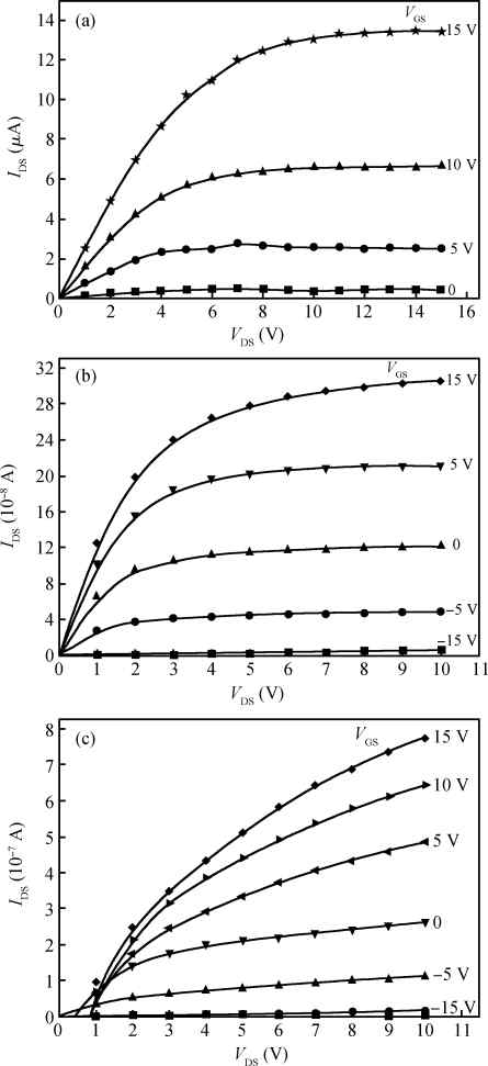
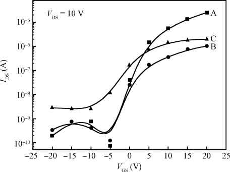
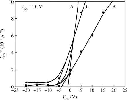
Table 1. The performance parameters of YIZO TFTs with different active layer thickness.
 DownLoad: CSV
| [1] | |
| [2] | |
| [3] | |
| [4] | |
| [5] | |
| [6] | |
| [7] | |
| [8] | |
| [9] | |
| [10] | |
| [11] | |
| [12] | |
| [13] | |
| [14] | |
| [15] | |
| [16] | |
| [17] | |
| [18] | |
| [19] | |
| [20] | |
| [21] | |
| [22] | |
| [23] | |
| [24] | |
| [25] | |
| [26] |


Article views: 4003 Times PDF downloads: 26 Times Cited by: 0 Times
Received: 23 February 2015 Revised: Online: Published: 01 September 2015
| Citation: |
Dandan Wang, Qingpu Wang, Hanbin Wang, Xijian Zhang, Liwei Wu, Fujie Li, Shuai Yuan. Characteristics of sputtered Y-doped IZO thin films and devices[J]. Journal of Semiconductors, 2015, 36(9): 093004. doi: 10.1088/1674-4926/36/9/093004
****
Dandan Wang and A Wang, Q P Wang, H B Wang, X J Zhang, L W Wu, F J Li, S Yuan. Characteristics of sputtered Y-doped IZO thin films and devices[J]. J. Semicond., 2015, 36(9): 093004. doi: 10.1088/1674-4926/36/9/093004.

|
| [1] | |
| [2] | |
| [3] | |
| [4] | |
| [5] | |
| [6] | |
| [7] | |
| [8] | |
| [9] | |
| [10] | |
| [11] | |
| [12] | |
| [13] | |
| [14] | |
| [15] | |
| [16] | |
| [17] | |
| [18] | |
| [19] | |
| [20] | |
| [21] | |
| [22] | |
| [23] | |
| [24] | |
| [25] | |
| [26] |

 WeChat ID
Journal of Semiconductors © 2017 All Rights Reserved 京ICP备05085259号-2


