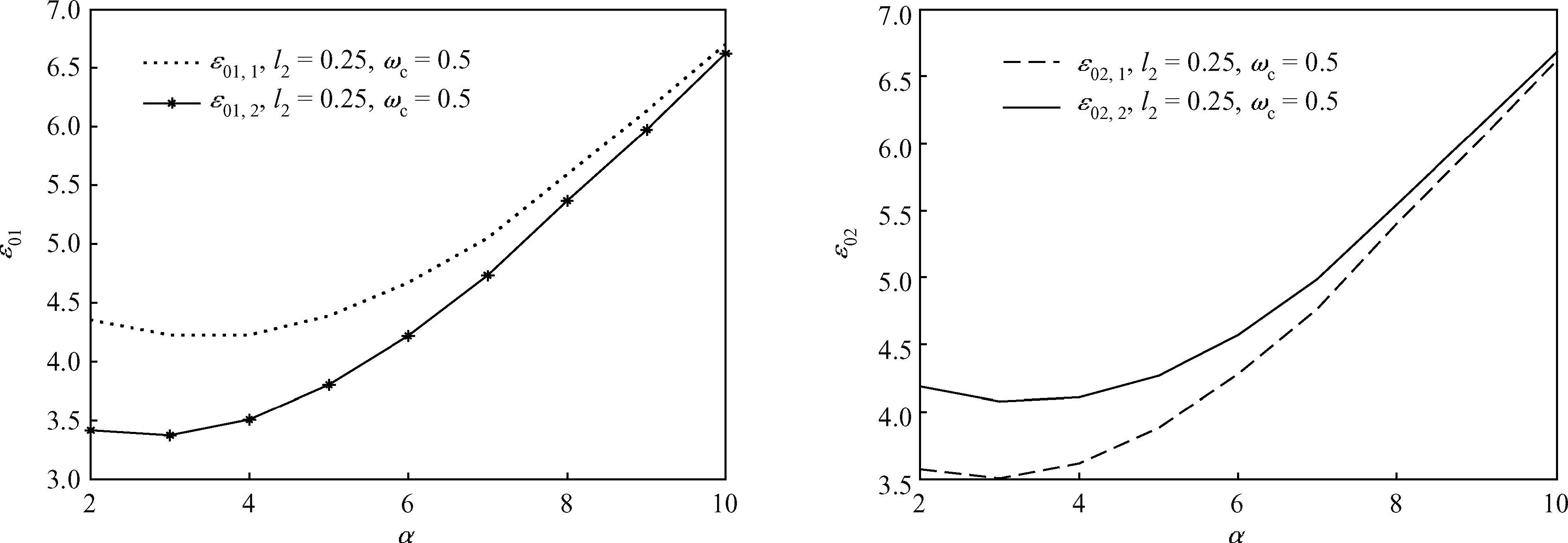
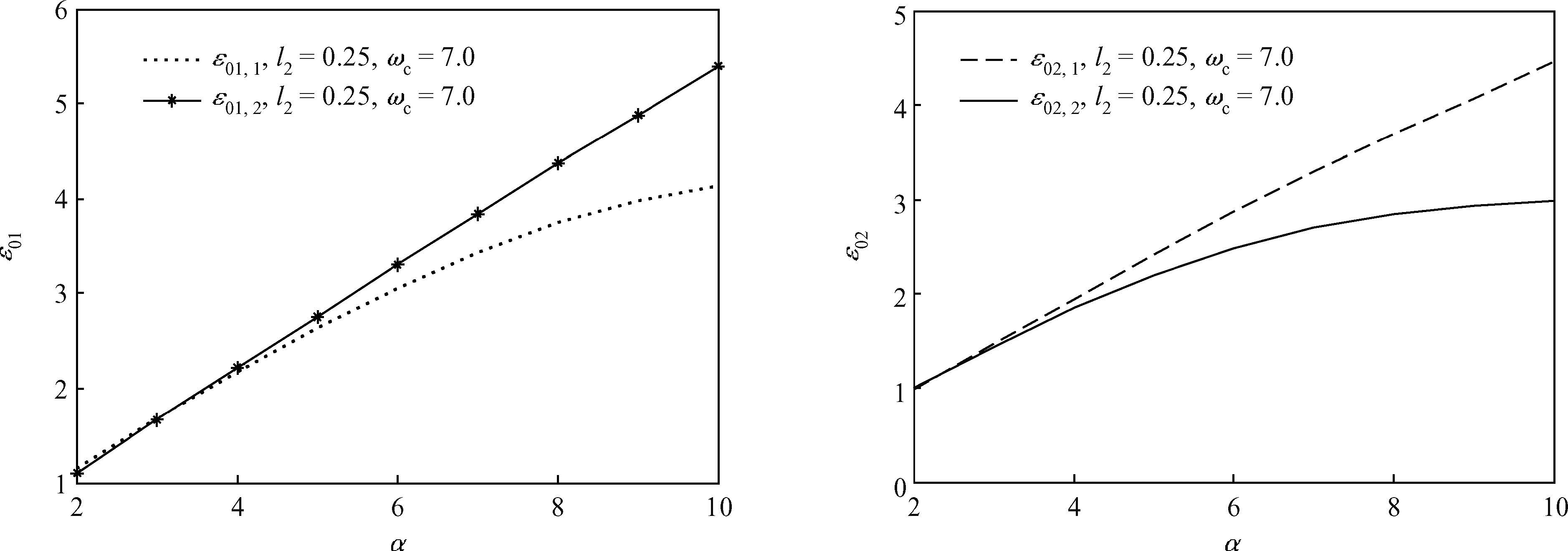
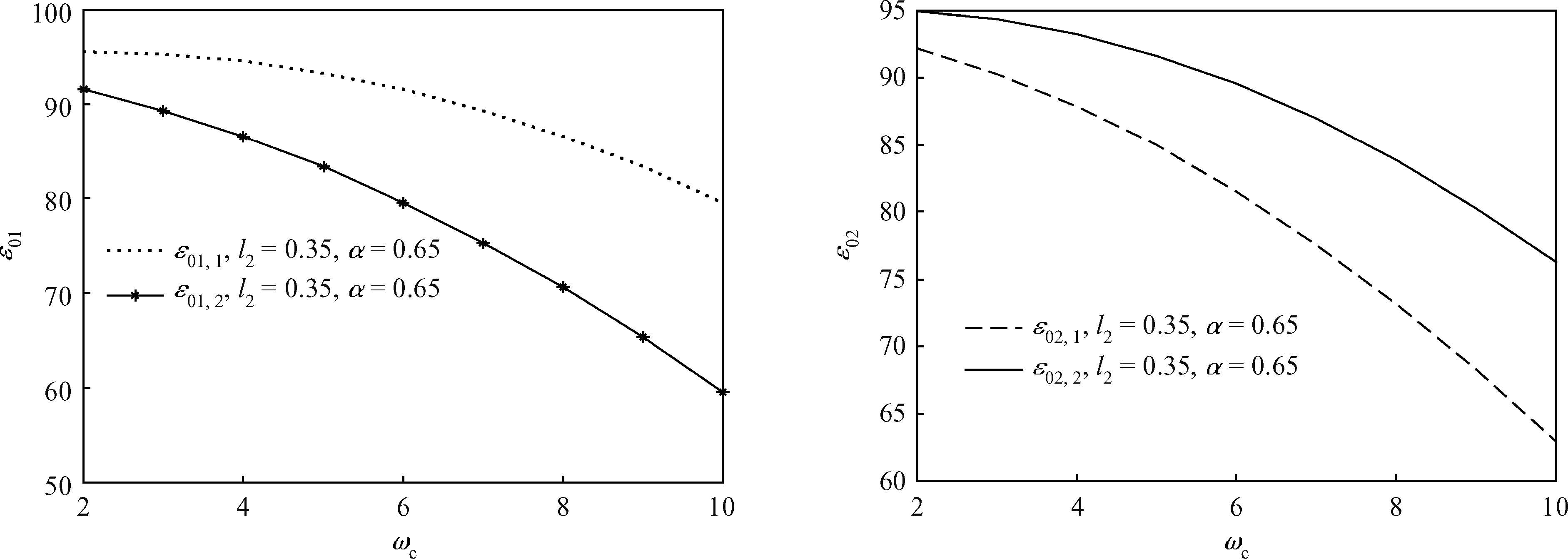
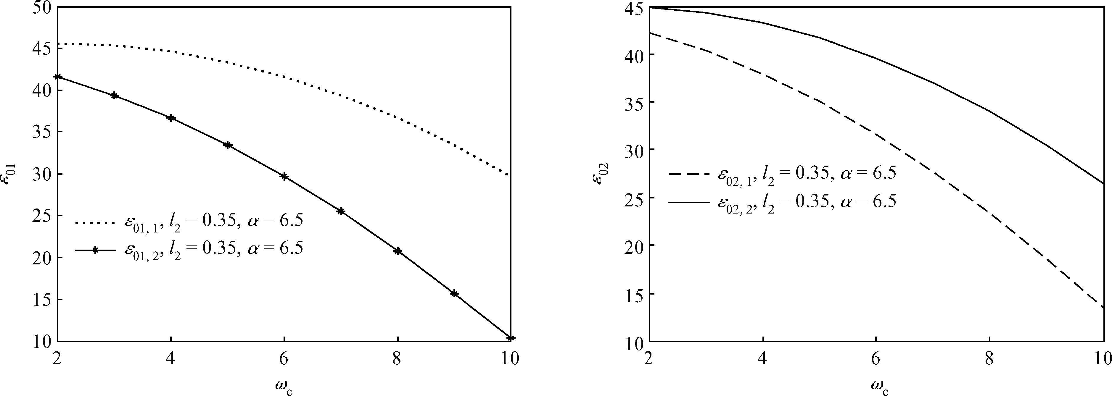
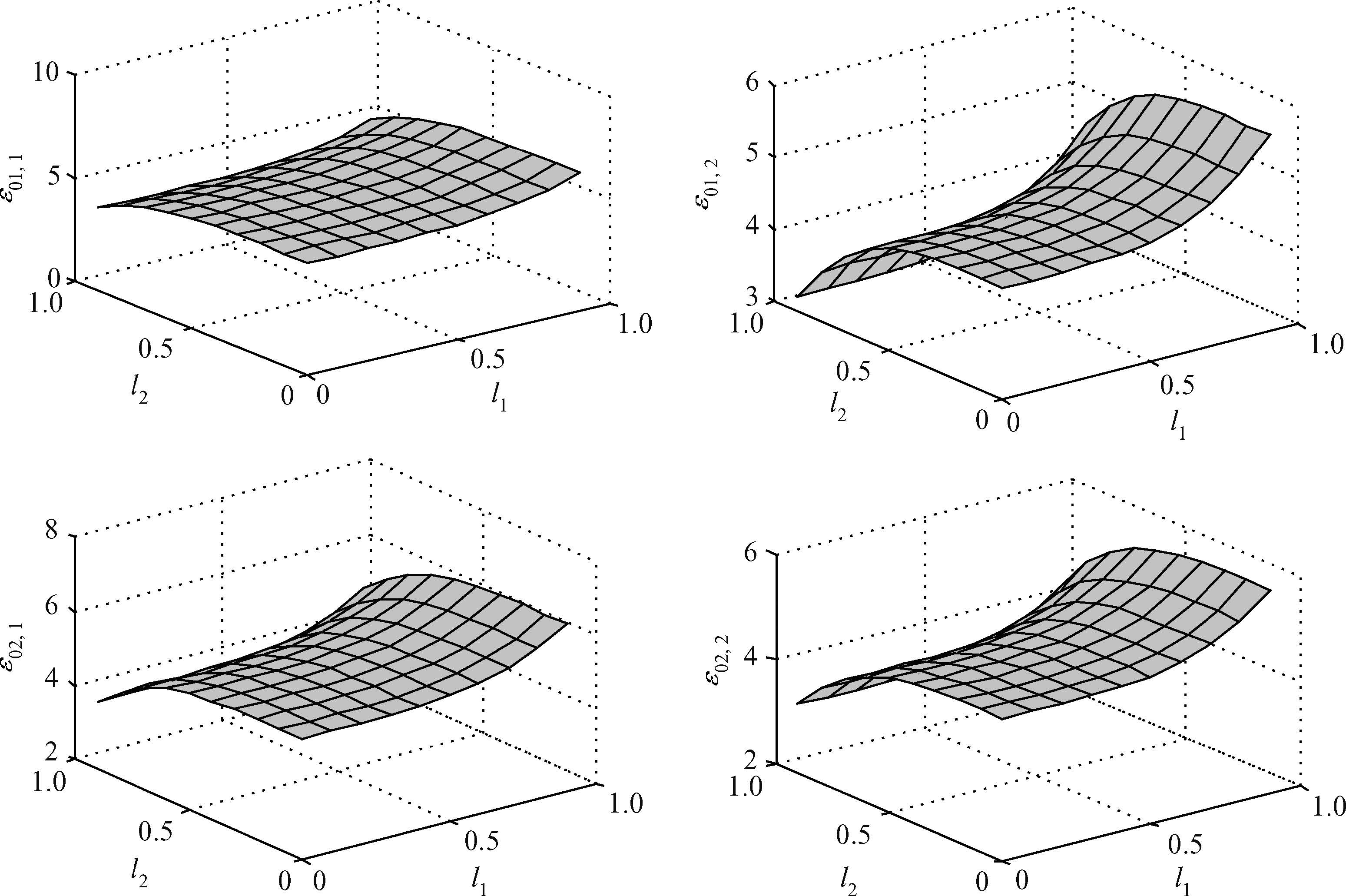
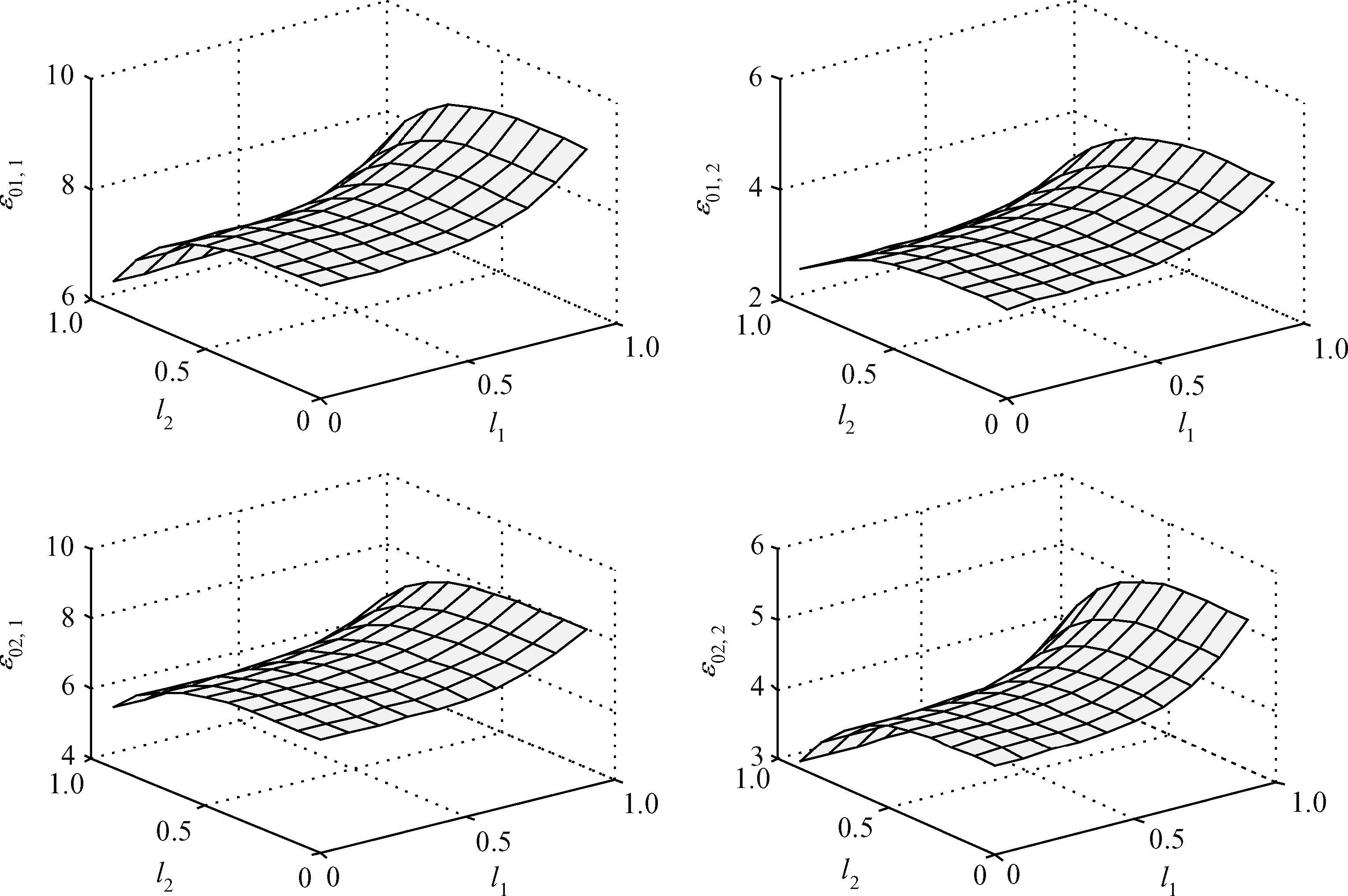
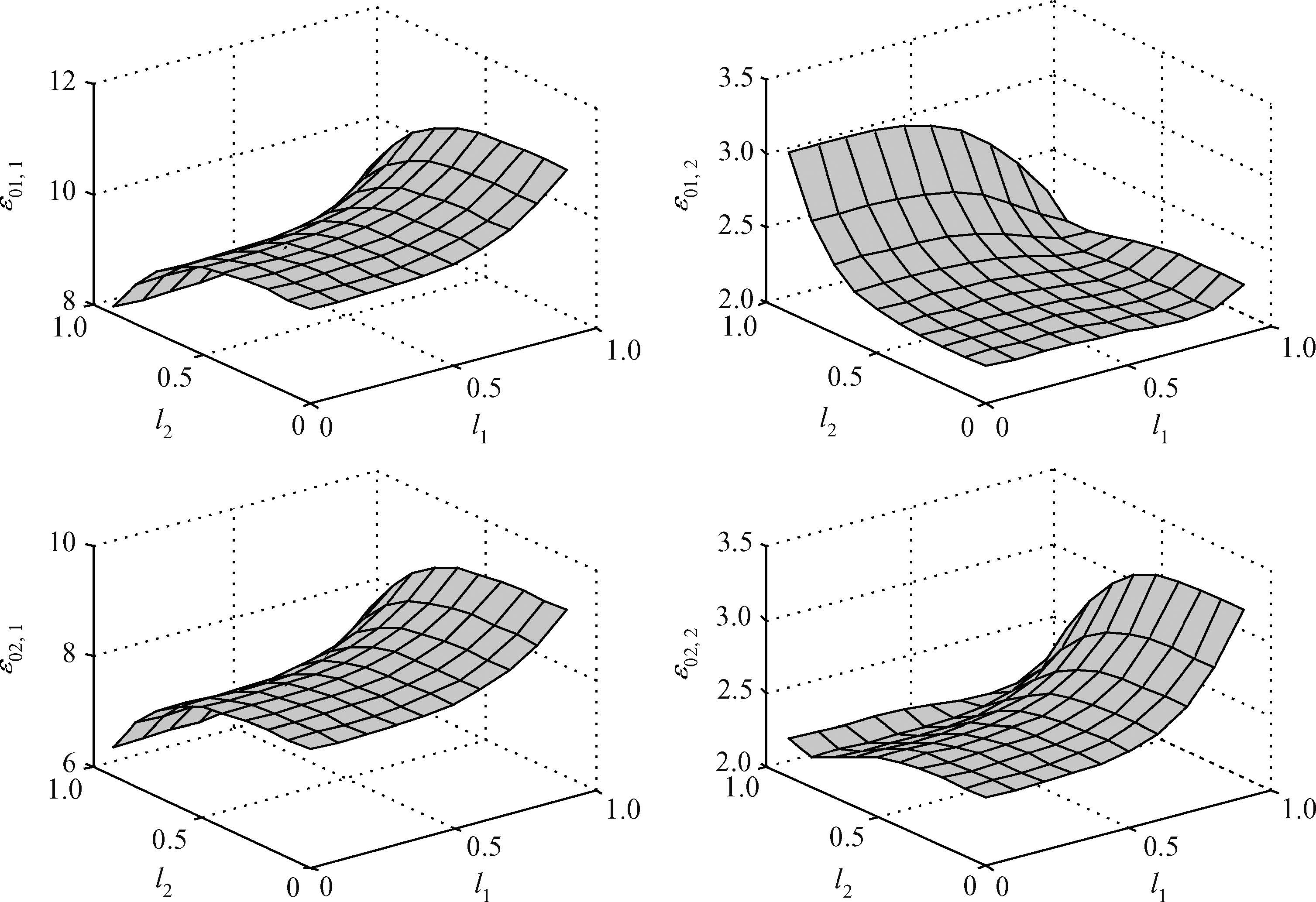
We investigate the influence of a magnetic field on the ground state energy of a polaron in a spherical semiconductor quantum dot (QD) using the modified LLP method. The ground state energy is split into sub-energy levels and there is a degeneracy of energy levels. It is also observed that the degenerate energy increase with the electron-phonon coupling constant and decrease with the magnetic field. The numerical results show that, under the influence of magnetic field and the interaction with the total momentum along the z-direction, the split energy increases and decreases with the longitudinal and the transverse confinement length, respectively.
Issue Browser
Volume 36, Issue 9,
Sep 2015
J. Semicond.
2015, 36(9): 092002 doi: 10.1088/1674-4926/36/9/092002

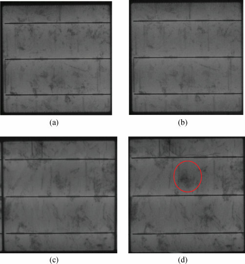
We try to find a fast and simple potential induced degradation effect (PID) test procedure for solar cells. With sodium chloride (NaCl) solution as Na+ source, PVB as lamination material, we can carry out the test for solar cells in 1 h. Solar cells with newly developed PID resistance process were also tested. The increase of reverse current of solar cells can be considered a key standard to determine if the solar cell was prone to PID. Moreover, it showed that the increase of reverse current for the PID resistance solar cell was less than 2. In addition, the test results of the solar cells fitted very well with that of the modules by standard procedure.

J. Semicond.
2015, 36(9): 093001 doi: 10.1088/1674-4926/36/9/093001

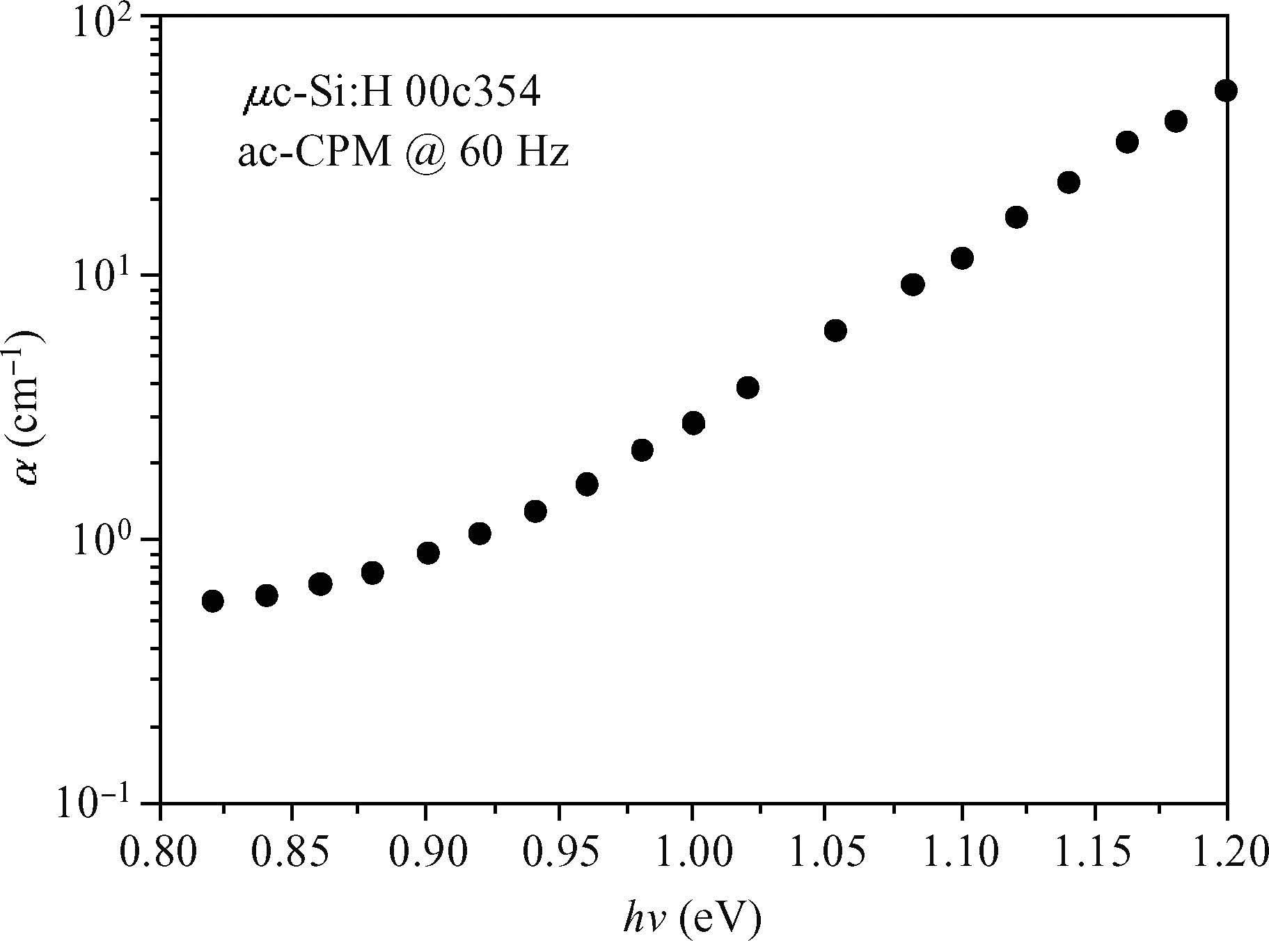
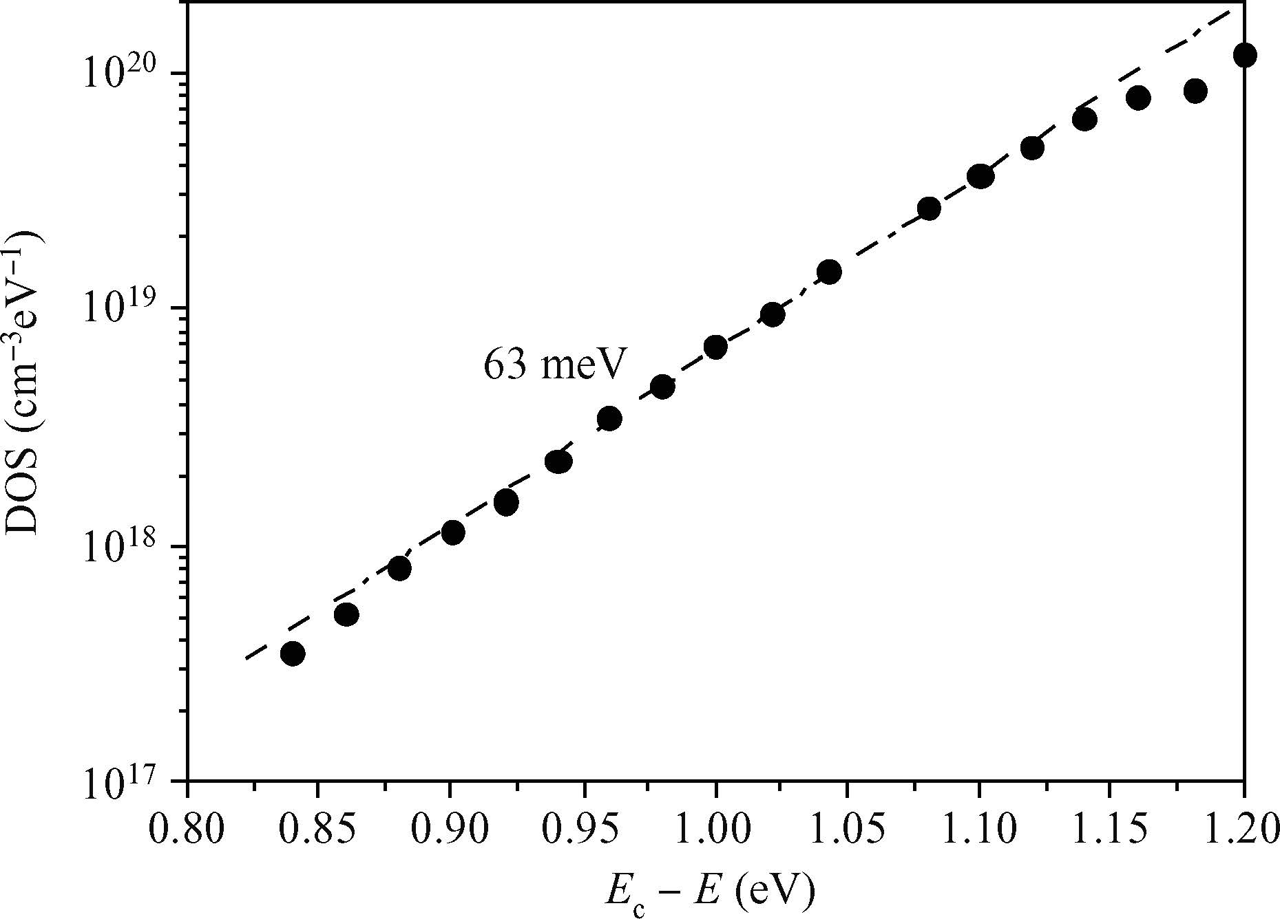
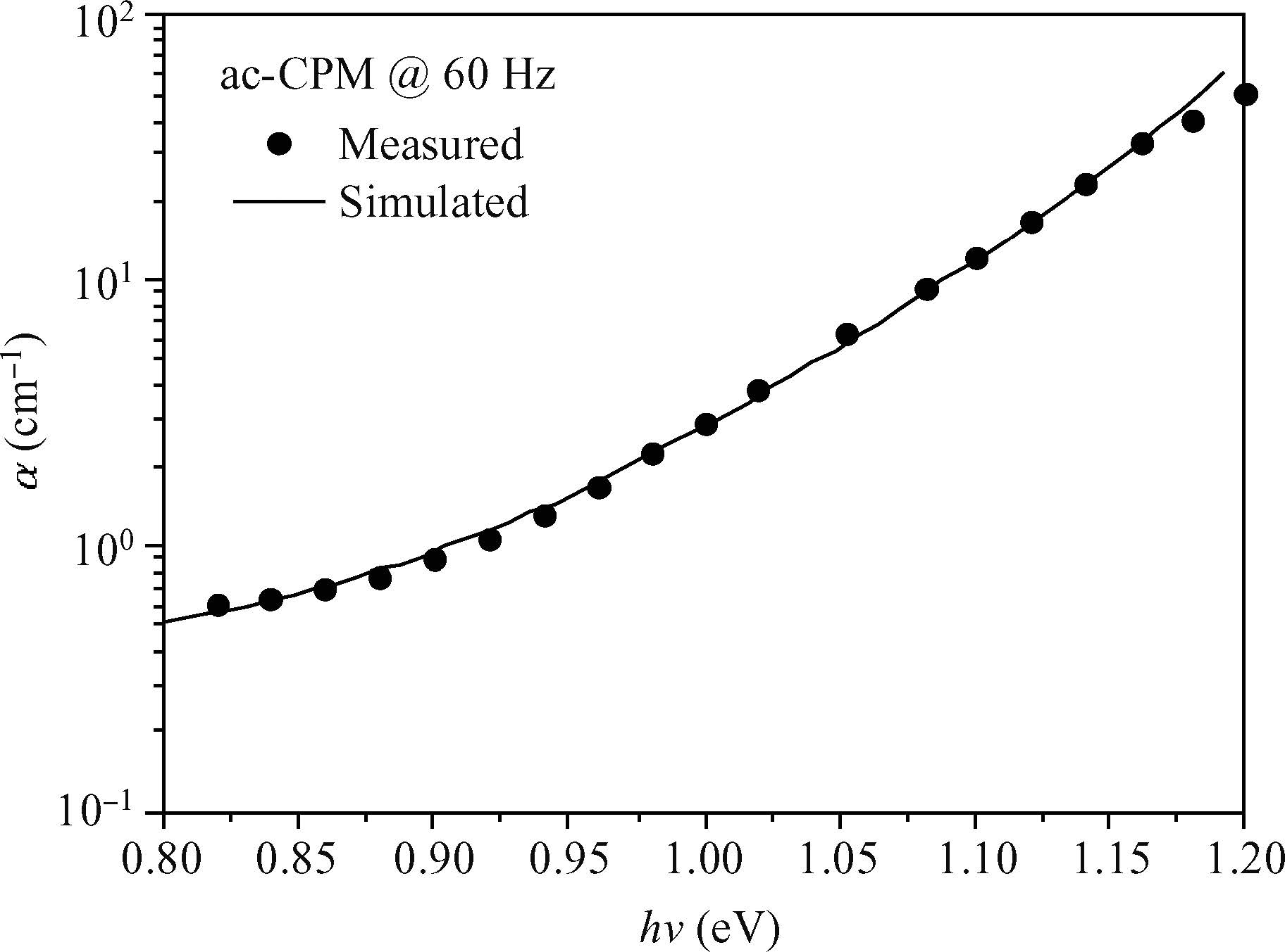
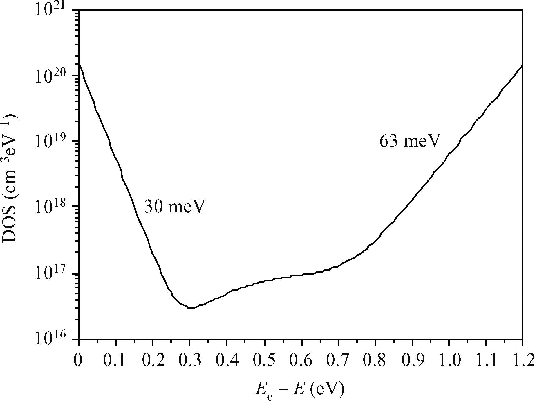
The constant photocurrent method in the ac-mode (ac-CPM) is used to determine the defect density of states (DOS) in hydrogenated microcrystalline silicon (μc-Si:H) prepared by very high frequency plasma-enhanced chemical vapor deposition (VHF-PECVD). The absorption coefficient spectrum (ac-α (hν)), is measured under ac-CPM conditions at 60 Hz. The measured ac-α (hν) is converted by the CPM spectroscopy into a DOS distribution covering a portion in the lower energy range of occupied states. We have found that the density of valence band-tail states falls exponentially towards the gap with a typical band-tail width of 63 meV. Independently, computer simulations of the ac-CPM are developed using a DOS model that is consistent with the measured ac-α (hν) in the present work and a previously measured transient photocurrent (TPC) for the same material. The DOS distribution model suggested by the measurements in the lower and in the upper part of the energy-gap, as well as by the numerical modelling in the middle part of the energy-gap, coincide reasonably well with the real DOS distribution in hydrogenated microcrystalline silicon because the computed ac-α (hν) is found to agree satisfactorily with the measured ac-α (hν).
J. Semicond.
2015, 36(9): 093002 doi: 10.1088/1674-4926/36/9/093002

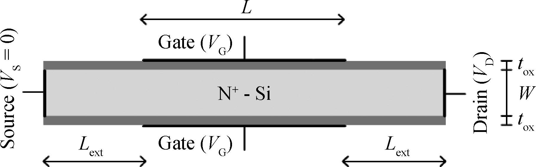
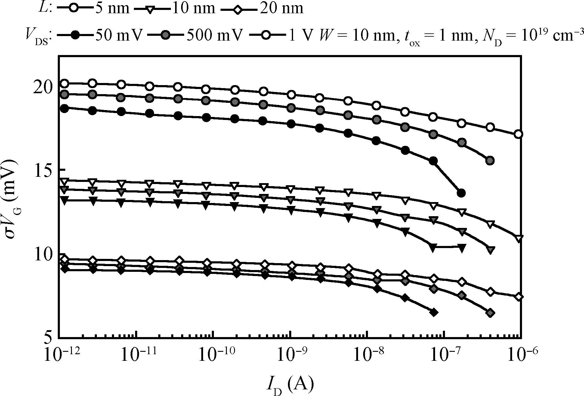
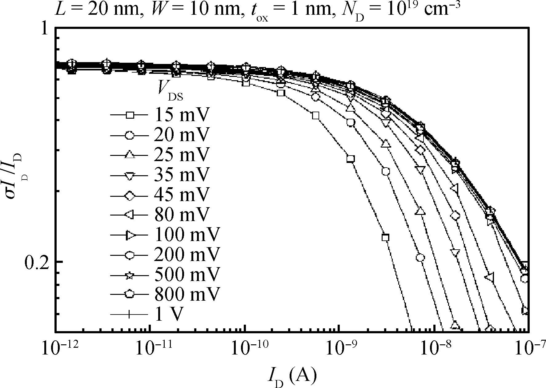
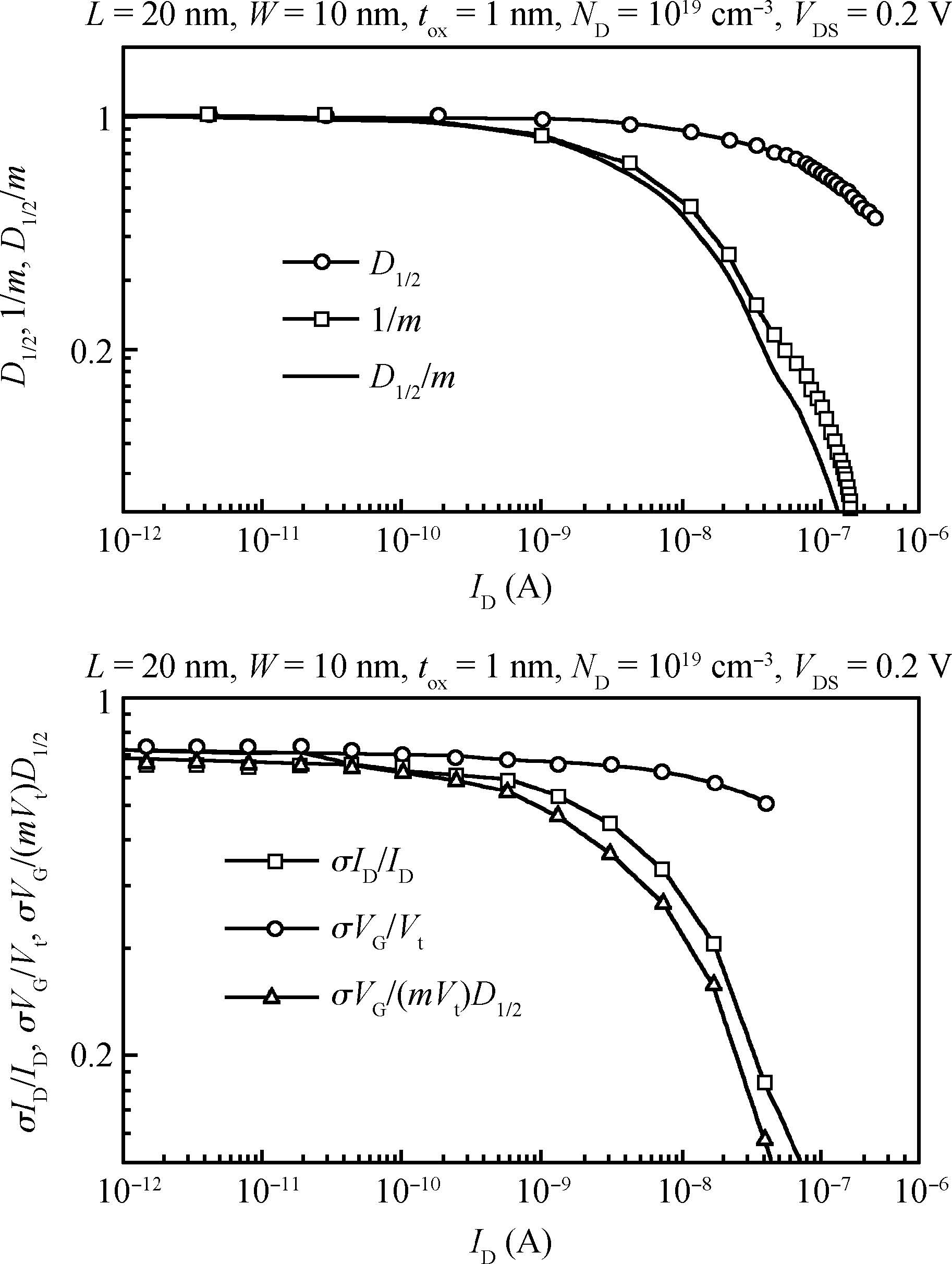
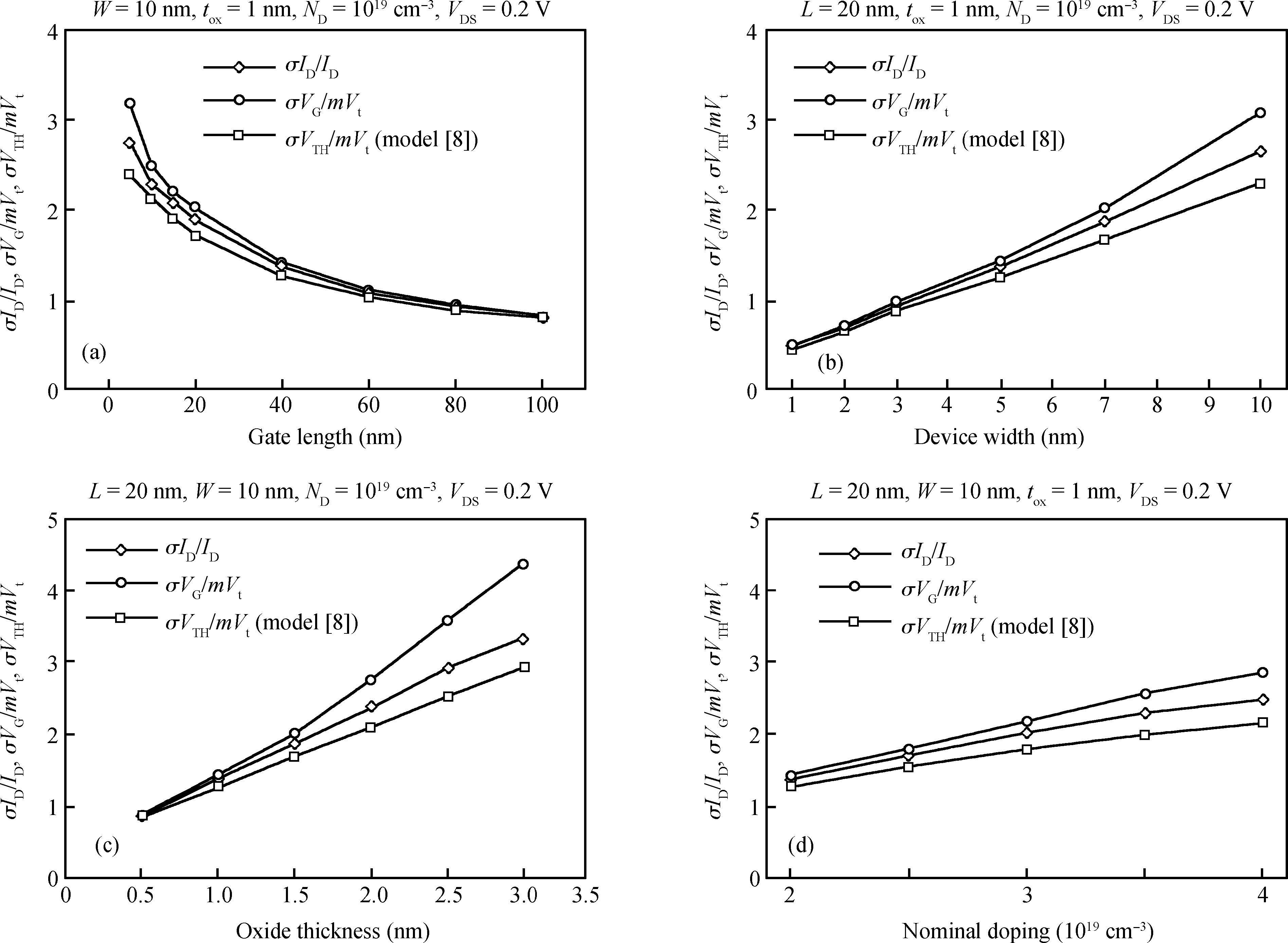
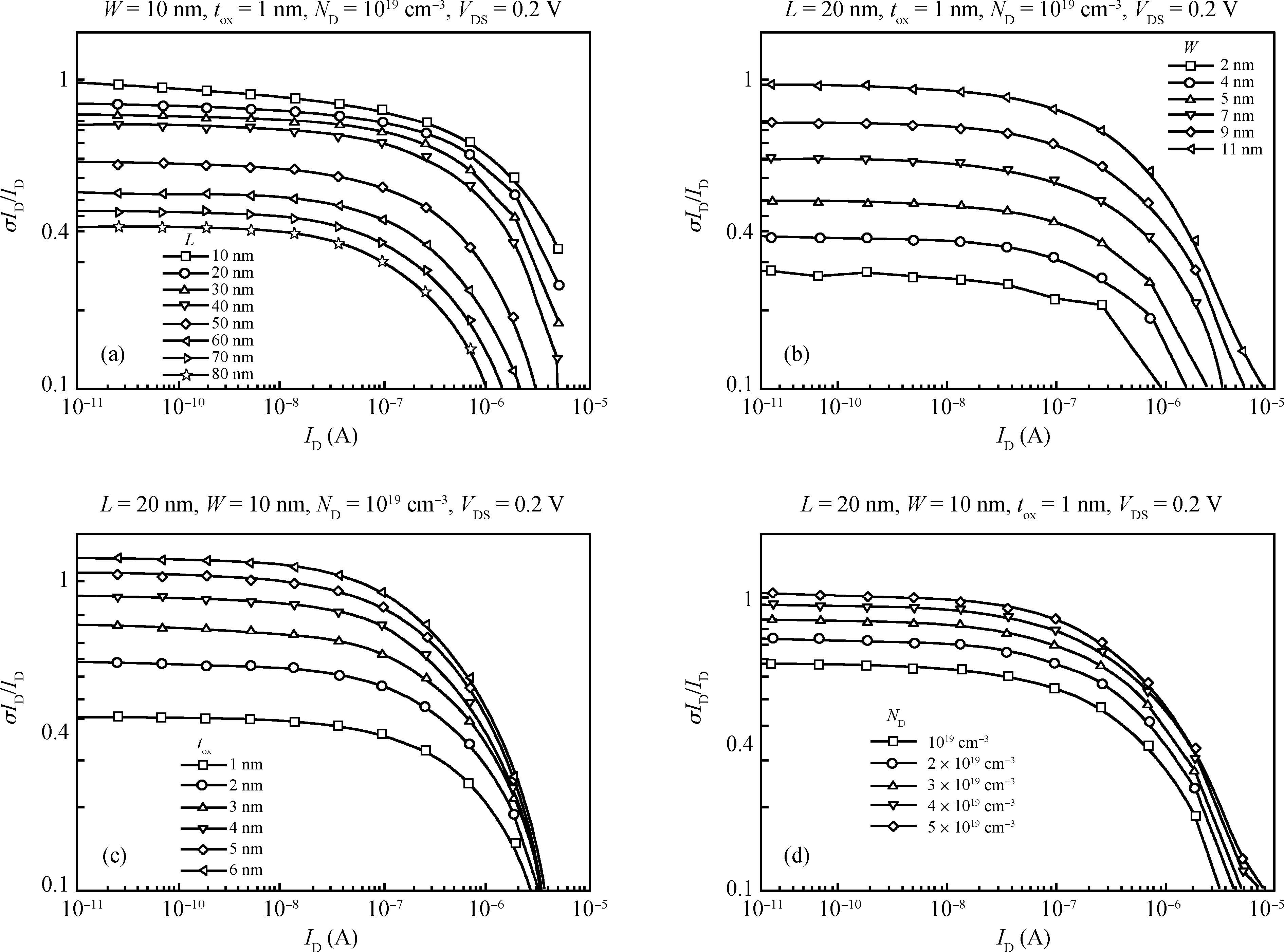
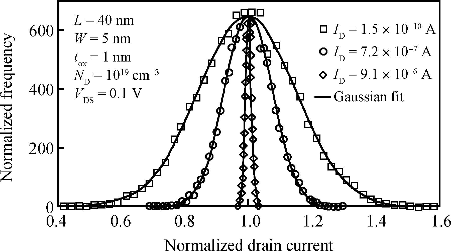
We investigate the effect of dopant random fluctuation on threshold voltage and drain current variation in a two-gate nanoscale transistor. We used a quantum-corrected technology computer aided design simulation to run the simulation (10000 randomizations). With this simulation, we could study the effects of varying the dimensions (length and width), and thicknesses of oxide and dopant factors of a transistor on the threshold voltage and drain current in subthreshold region (off) and overthreshold (on). It was found that in the subthreshold region the variability of the drain current and threshold voltage is relatively fixed while in the overthreshold region the variability of the threshold voltage and drain current decreases remarkably, despite the slight reduction of gate voltage diffusion (compared with that of the subthreshold). These results have been interpreted by using previously reported models for threshold current variability, load displacement, and simple analytical calculations. Scaling analysis shows that the variability of the characteristics of this semiconductor increases as the effects of the short channel increases. Therefore, with a slight increase of length and a reduction of width, oxide thickness, and dopant factor, we could correct the effect of the short channel.

J. Semicond.
2015, 36(9): 093003 doi: 10.1088/1674-4926/36/9/093003

The unintentional carbon doping concentration of GaN films grown by low pressure metal organic chemical vapor deposition (LP-MOCVD) depends strongly on the growth rate. The concentration of carbon is varied from 2.9 × 10¹⁷ to 5.7 × 1018 cm-3 when the growth rate increases from 2.0 to 7.2 μm/h, as detected by secondary ion mass spectroscopy. It is shown that the presence of N vacancies give rises to high carbon concentration. We show that a reduction of the carbon concentration by one order of magnitude compared to the regular sample with nearly same growth rate can be achieved by operating at an extremely high NH3 partial pressure during growth. The intensity ratios of yellow and blue luminescence to band edge luminescence in the samples are found to depend significantly on carbon concentration. The present results demonstrate direct and quantitative evidence that the carbon related defects are the origin of yellow and blue luminescence.


J. Semicond.
2015, 36(9): 093004 doi: 10.1088/1674-4926/36/9/093004

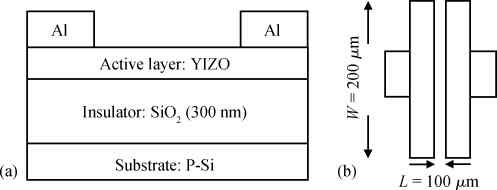
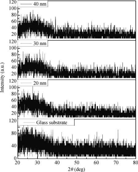
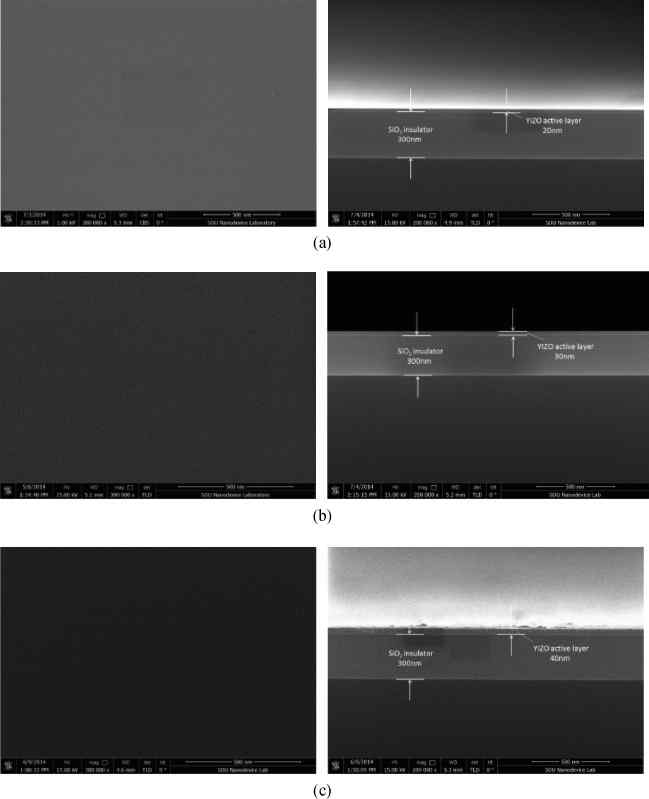
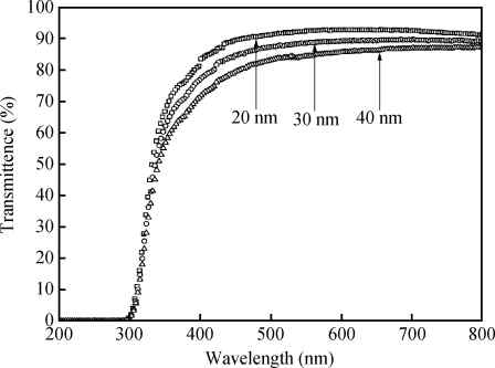
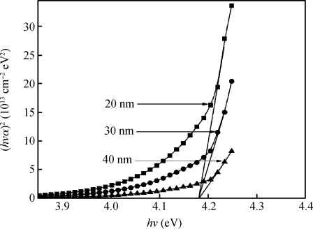
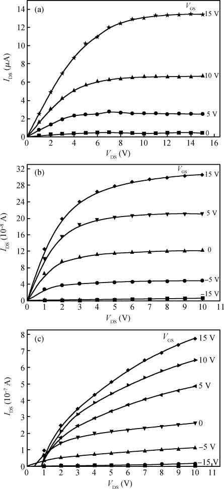
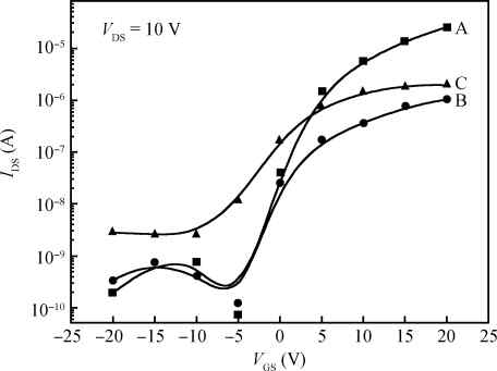
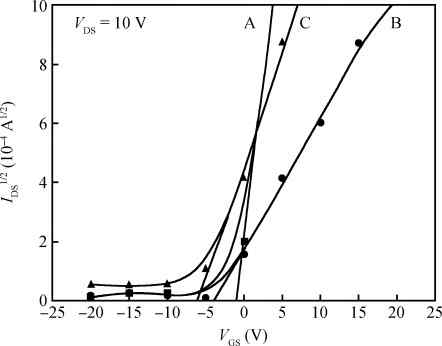
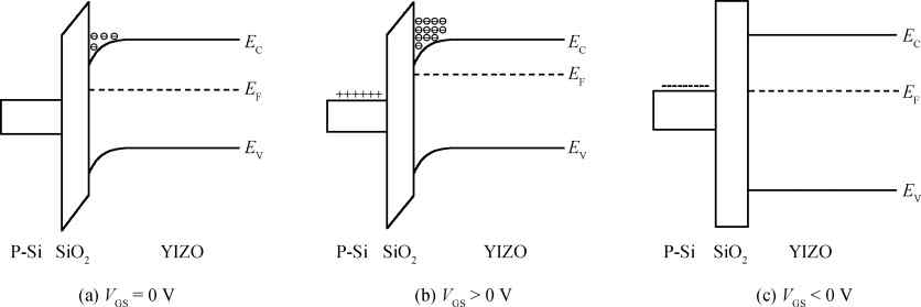
Yttrium-doped IZO (YIZO) thin films with different thickness have been prepared on soda-lime glass (SLG) and P-Si substrates by radio frequency magnetron sputtering at room temperature. Structural morphology and optical properties of the films have been investigated. YIZO thin film transistors (TFTs) with the bottom-gate-structure are fabricated on P-Si substrates. The output and transfer characteristics of YIZO-TFT have been studied. It has been found that all YIZO thin films prepared at room temperature are amorphous, and the YIZO TFTs exhibit n-channel depletion mode. YIZO-TFT with active layer thickness of 20 nm shows an on/off ratio over 105, a sub-threshold swing of 2.20 V/decade at a low operating voltage of -1.0 V, and saturation mobility values over 0.57 cm2/(V· s).
J. Semicond.
2015, 36(9): 093005 doi: 10.1088/1674-4926/36/9/093005

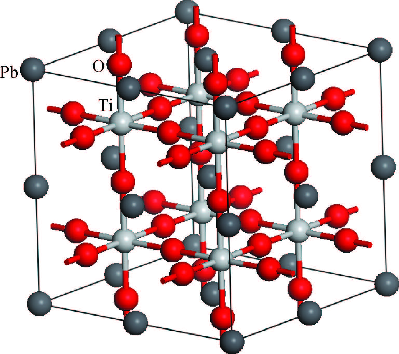
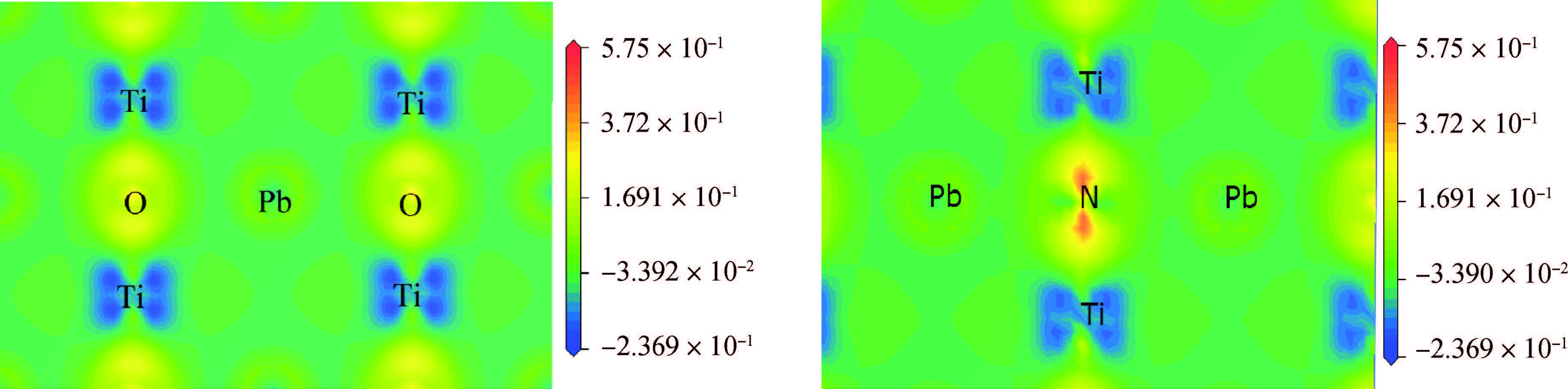
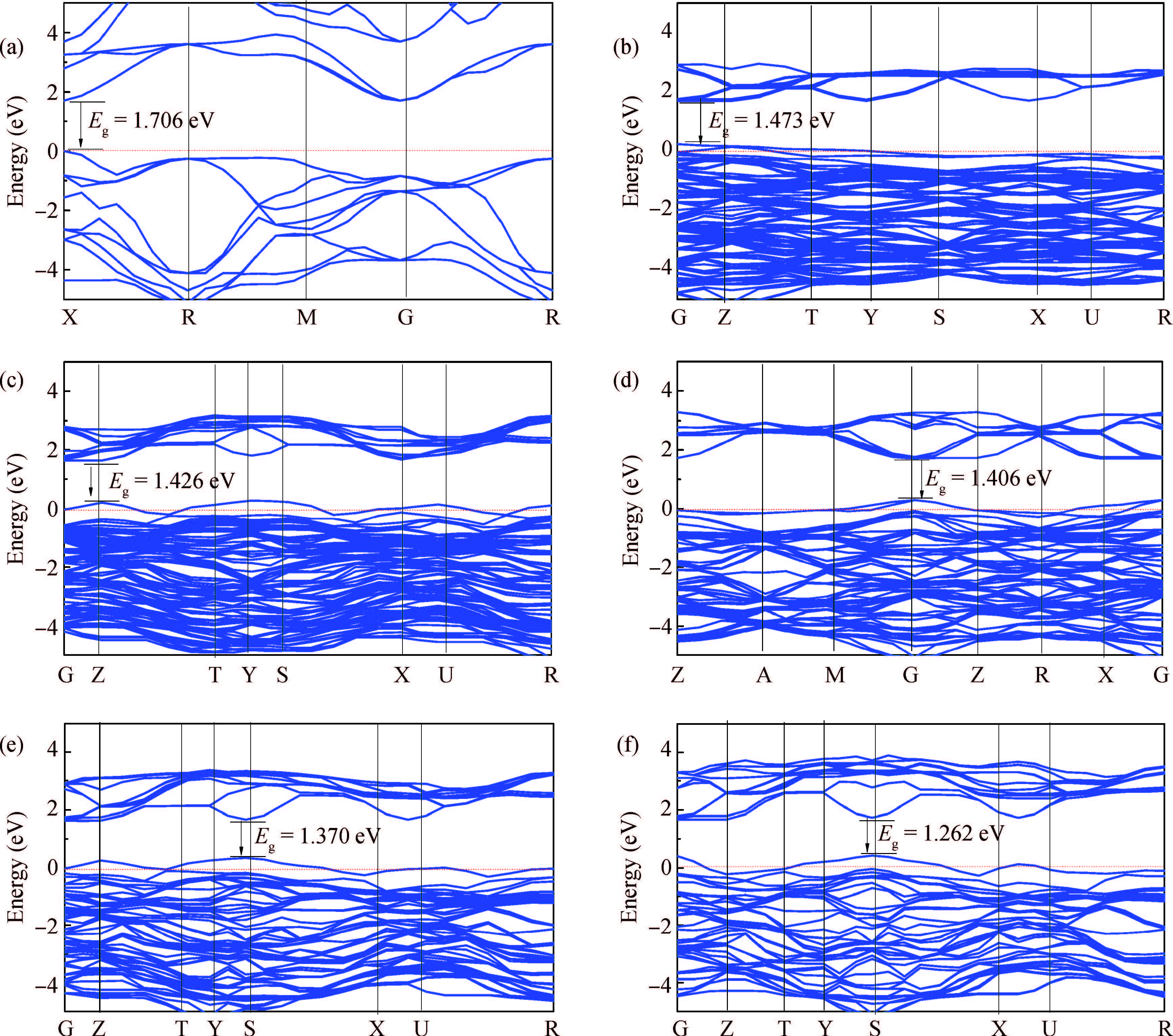
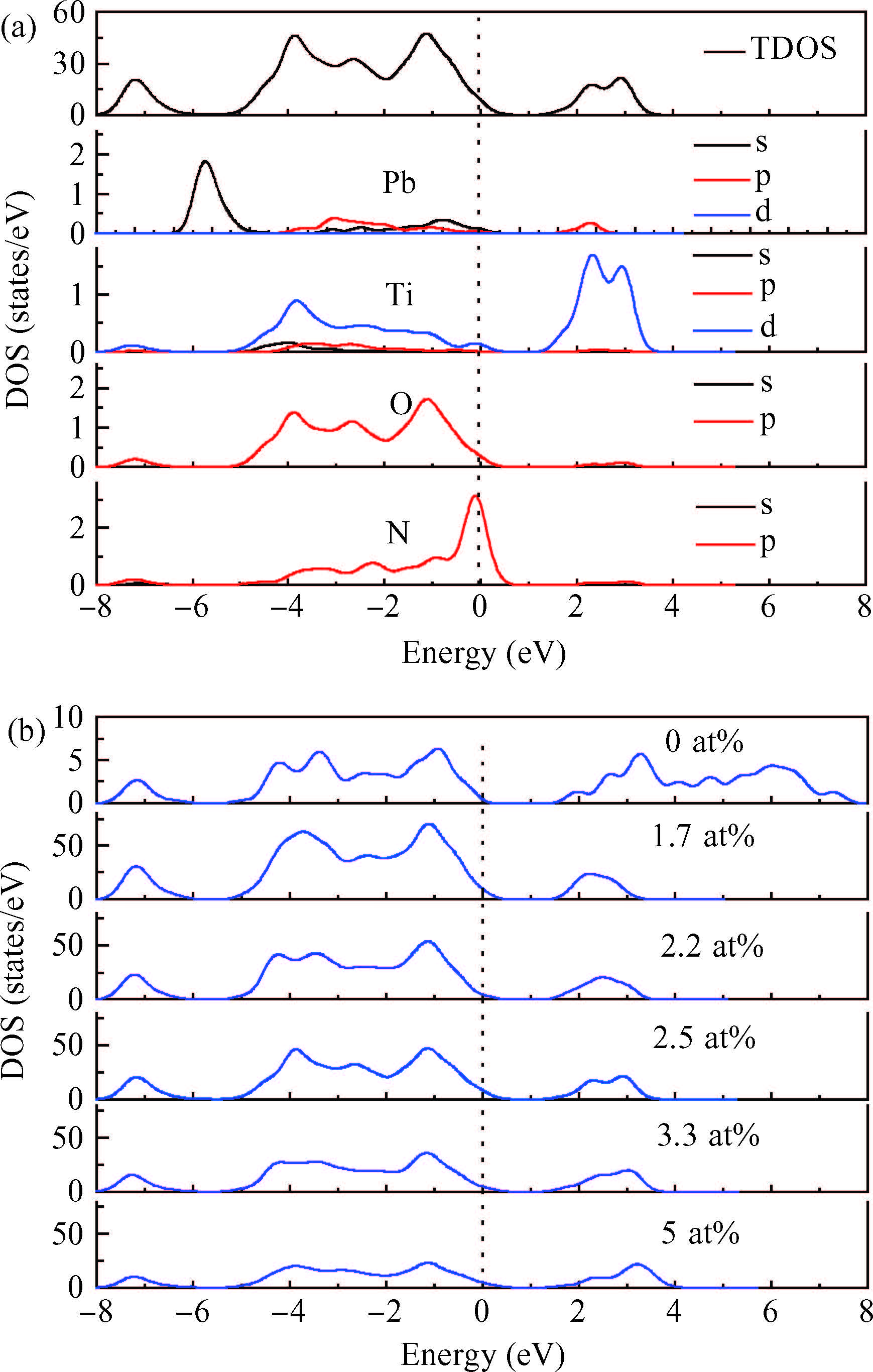
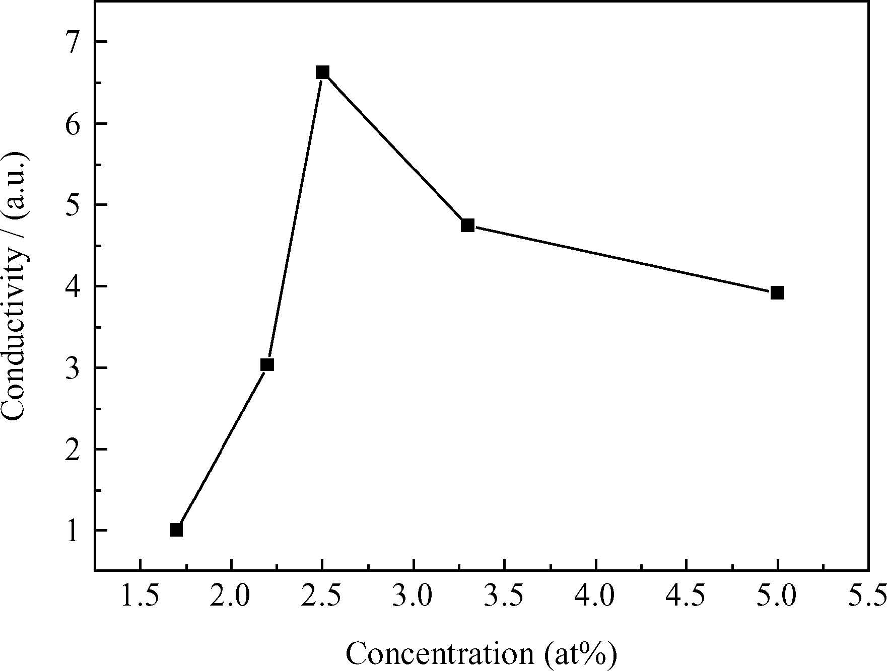
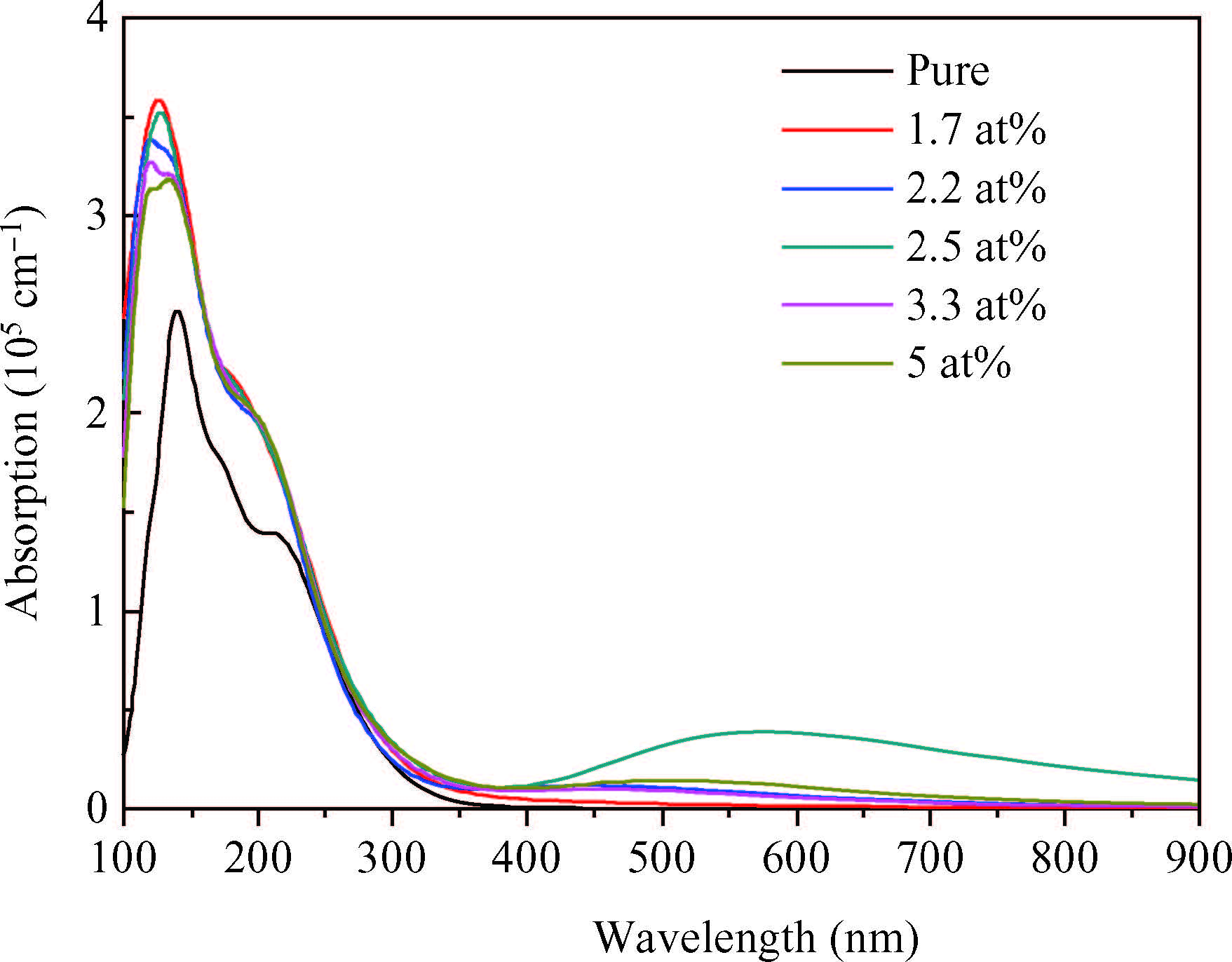
The p-type N-doped PbTiO3 with different doping concentrations have been studied by first-principles calculations. The charge density differences, band structures, density of states and optical properties have been investigated. After an oxygen atom is substituted by a nitrogen atom in the crystals, the valance bands move to high energy levels and the Fermi energy level gets into the top of the valance bands. Results show that the values of the band gaps are decreased and the stability is weakened when the N concentration increases. The 2.5 at% N-doped PbTiO3 shows the best p-type conductivity and the visible-light absorption can be enhanced most at this doping concentration, which is necessary in semiconductors or photocatalysts.
J. Semicond.
2015, 36(9): 093006 doi: 10.1088/1674-4926/36/9/093006

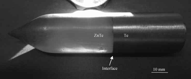
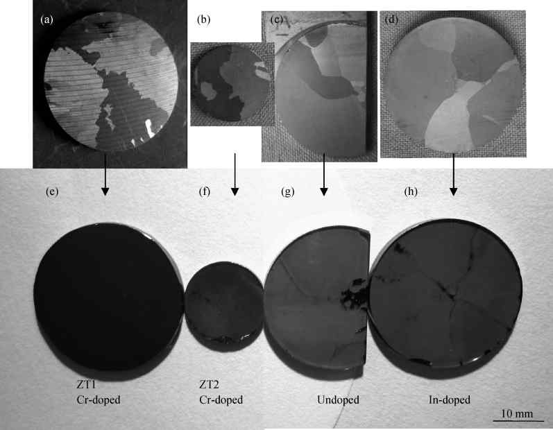
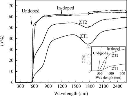
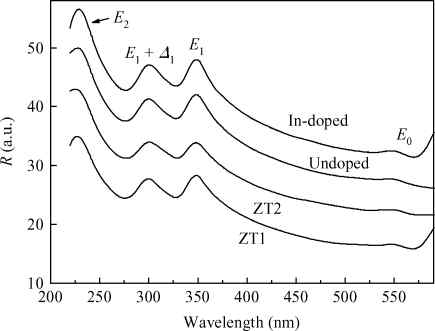
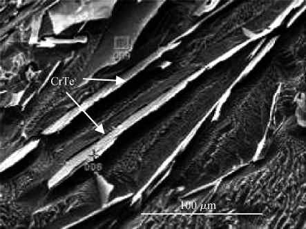
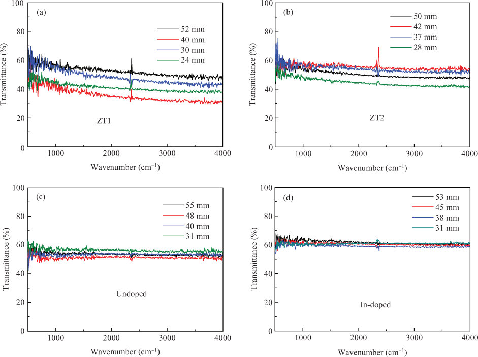
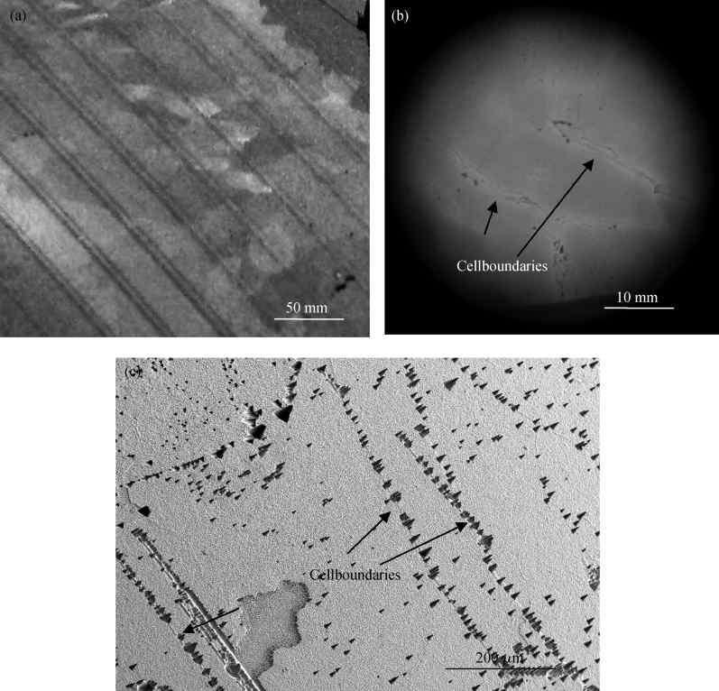
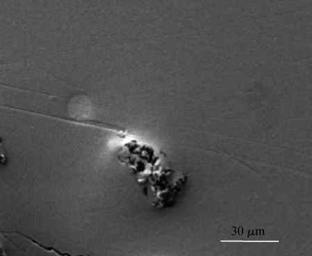
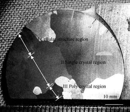
The properties of undoped, Cr-doped, and In-doped bulk ZnTe crystals grown by the TGSG method were compared. Cr/In-doping leads to a slight red-shift of the absorption edge. Cr-doping also creates two characteristic absorption bands, centered at about 1750 nm and beneath the fundamental absorption edge. However, the fundamental reflectance spectra are not sensitive to the dopants. The resistivity of undoped, Cr-doped, and In-doped ZnTe is about 102 Ω · cm, 103 Ω · cm, and 108 Ω · cm, respectively. Only In-doped ZnTe has an IR transmittance higher than 60% in the range of 500 to 4000 cm-1. However, the IR transmittance of Cr-doped ZnTe is very low and decreases greatly as the wavenumber increases, which is mainly attributed to the scattering effects caused by some defects generated by Cr-doping.
J. Semicond.
2015, 36(9): 094001 doi: 10.1088/1674-4926/36/9/094001

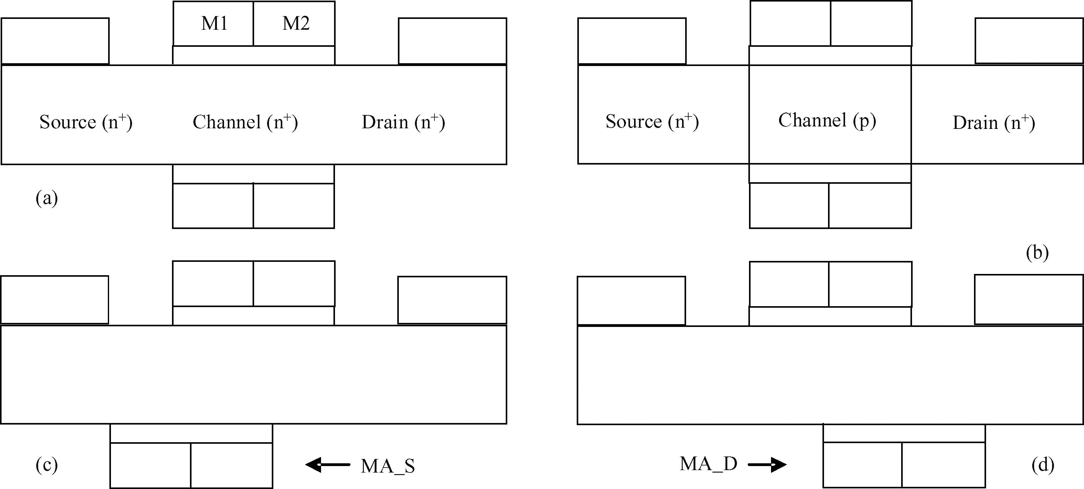
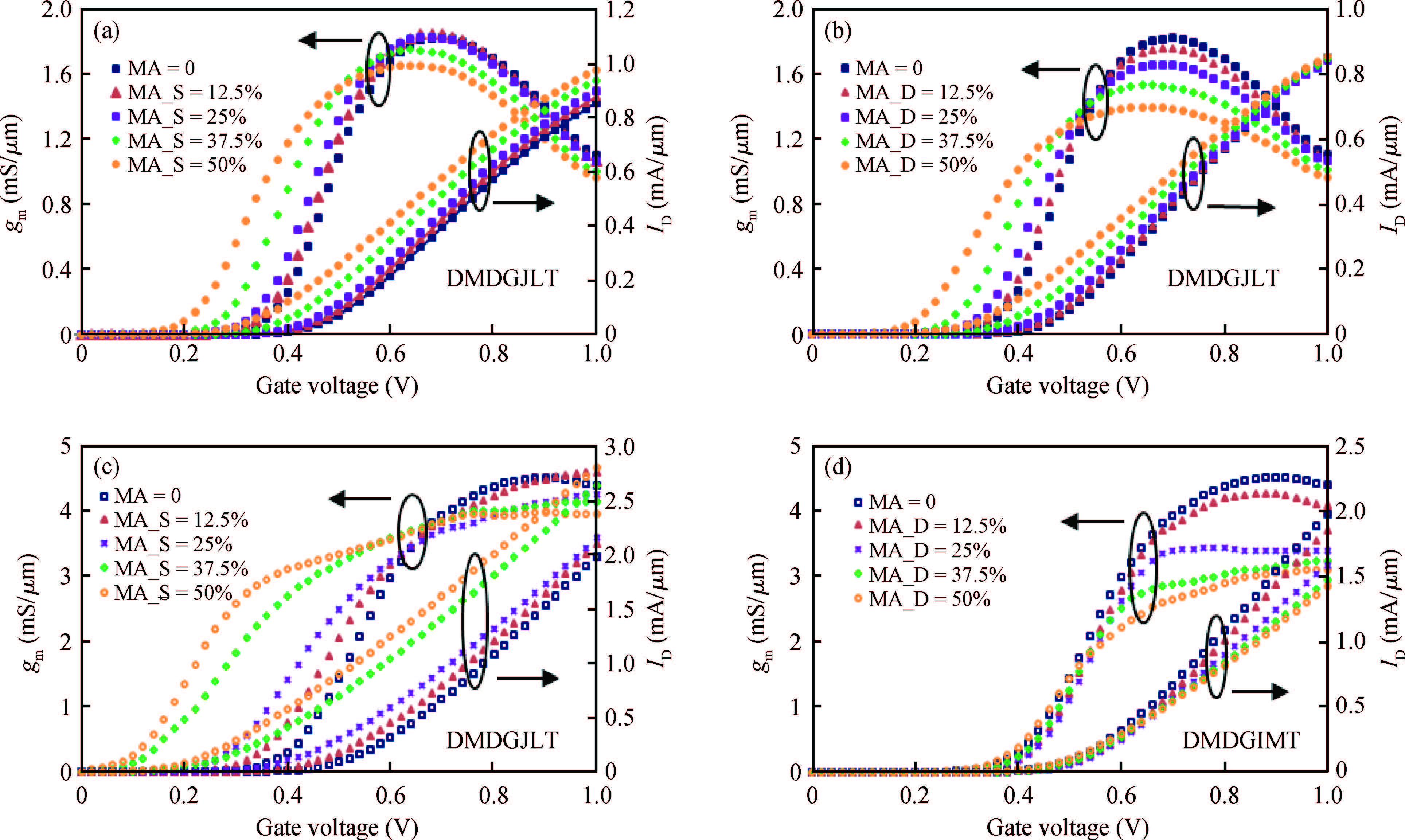
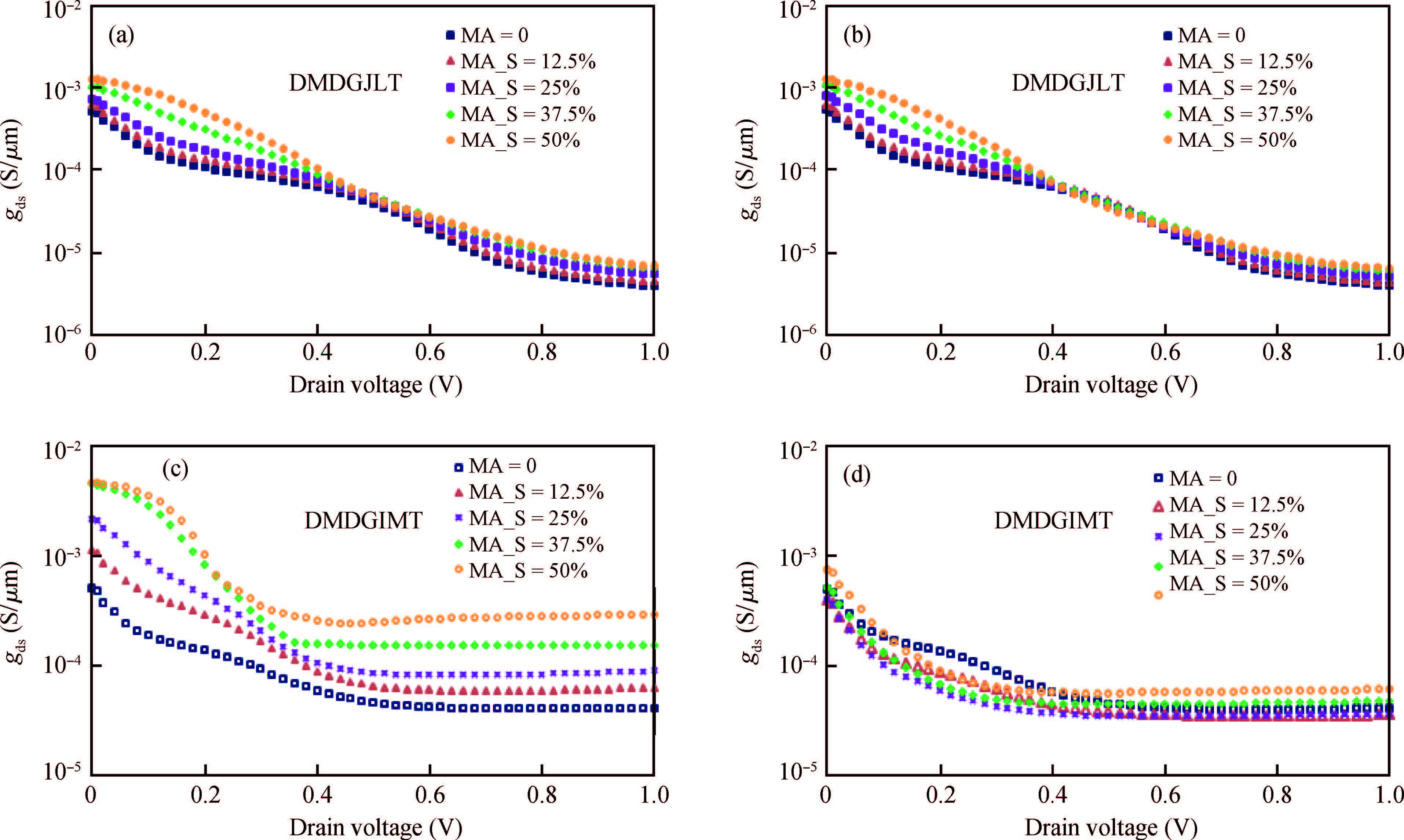
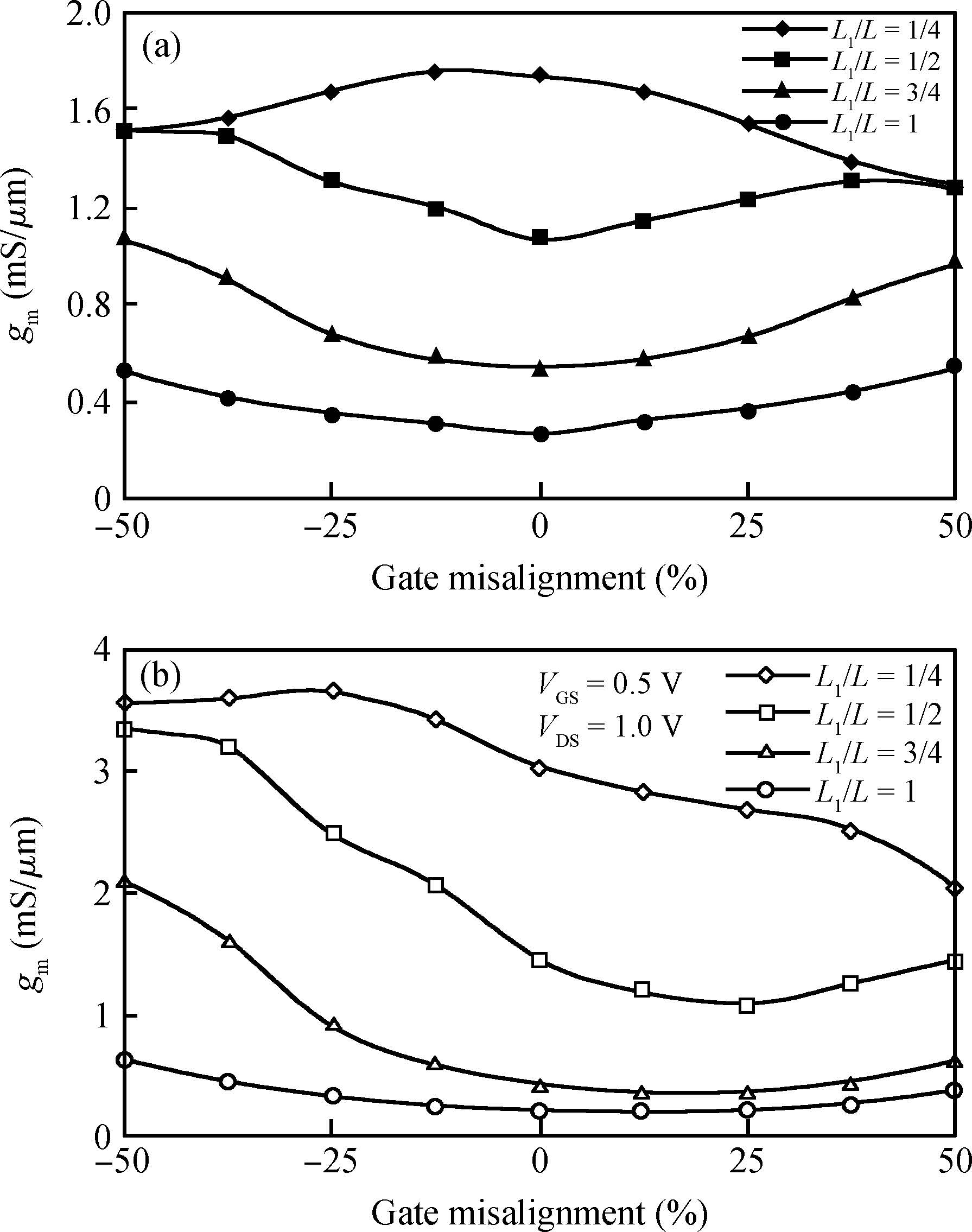
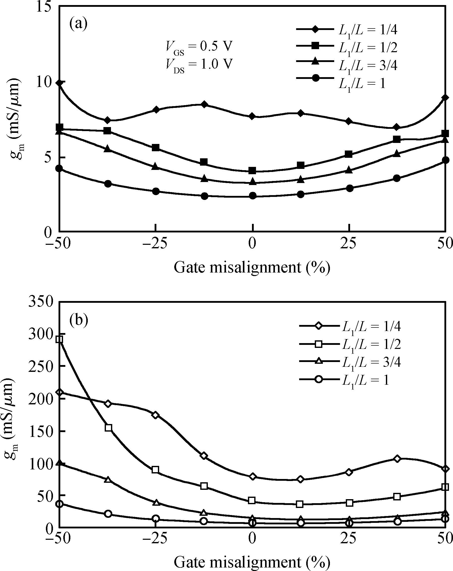
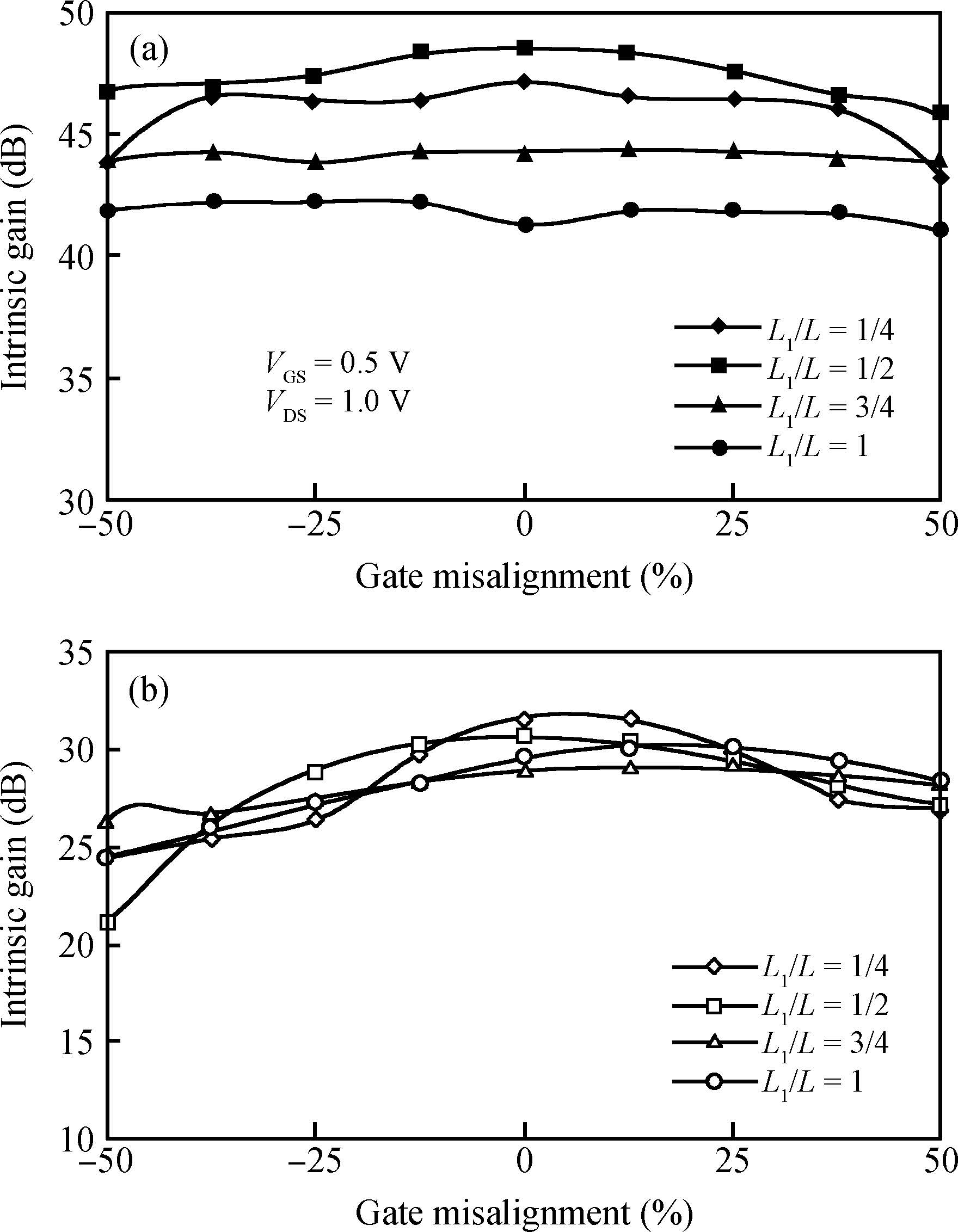
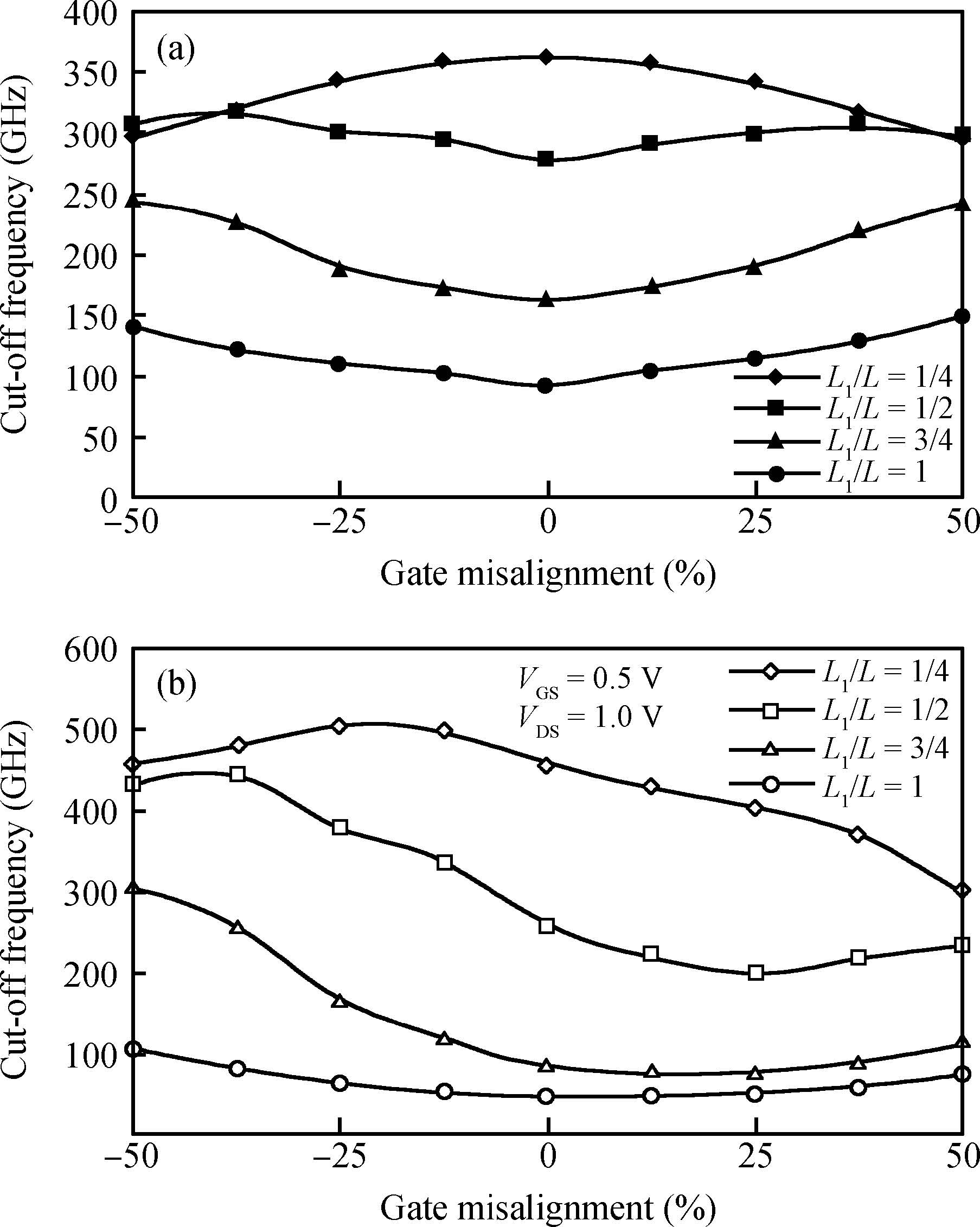
The analog performance of gate misaligned dual material double gate junctionless transistor is demonstrated for the first time. The cases considered are where misalignment occurs towards source side and towards drain side. The analog performance parameters analyzed are: transconductance, output conductance, intrinsic gain and cut-off frequency. These figures of merits (FOMs) are compared with a dual material double gate inversion mode transistor under same gate misalignment condition. The impacts of different length of control gate (L1) for a given gate length (L) are also studied and the optimum lengths L1 under misalignment condition to have better analog FOMs and high tolerance to misalignment are presented.
J. Semicond.
2015, 36(9): 094002 doi: 10.1088/1674-4926/36/9/094002

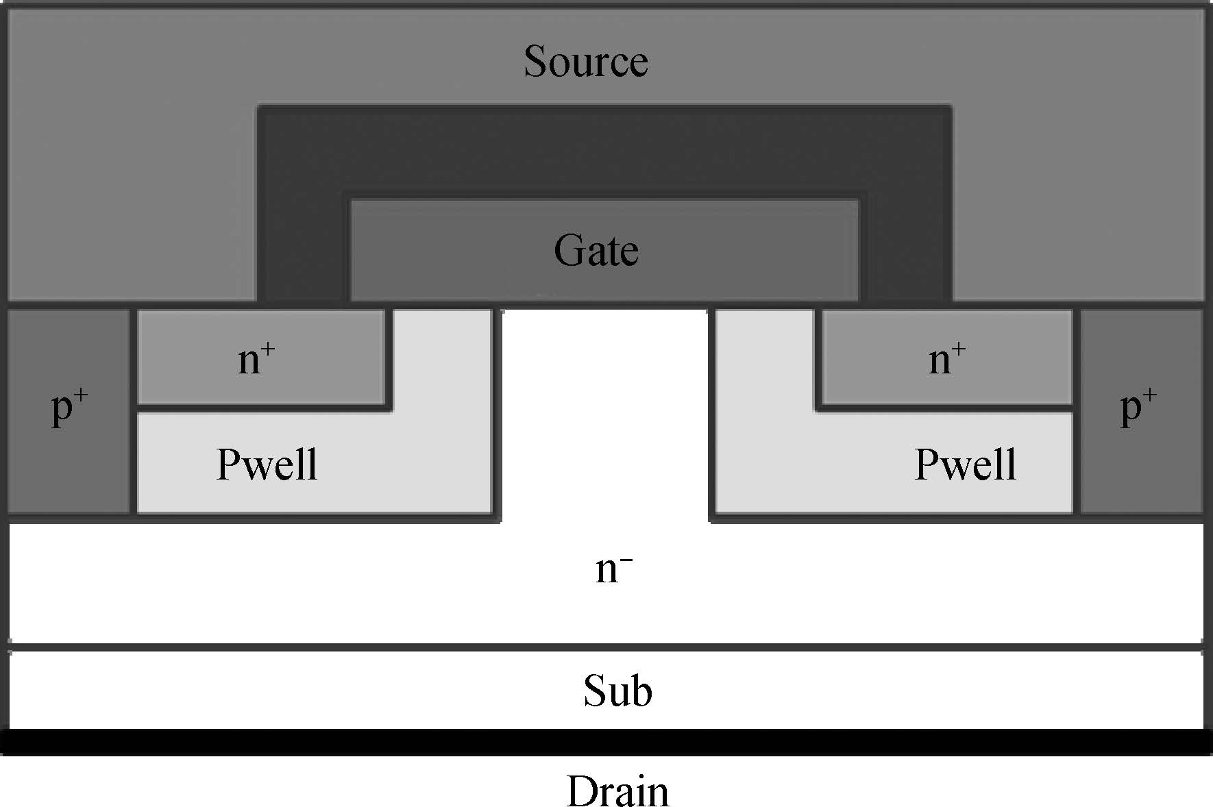
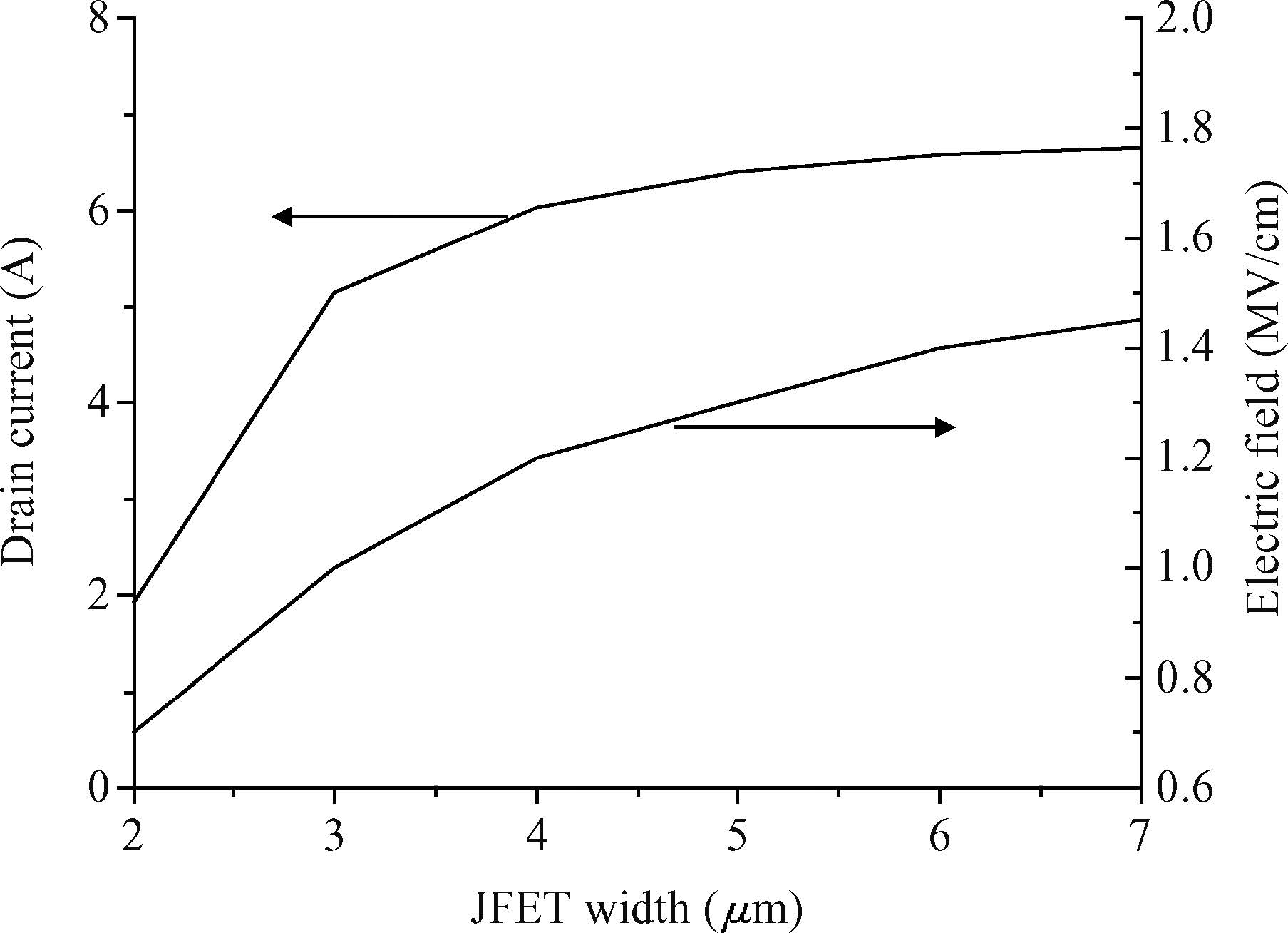
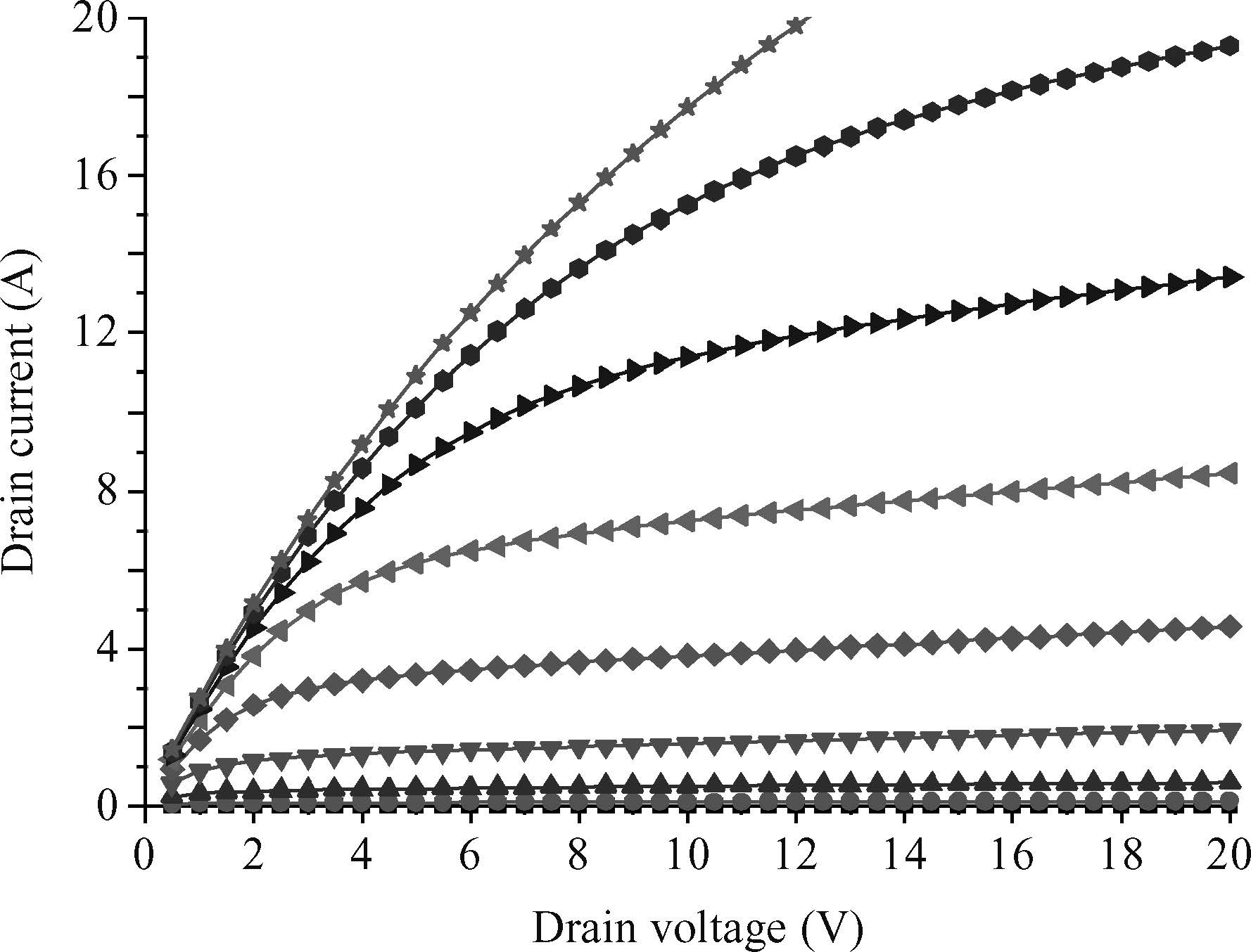
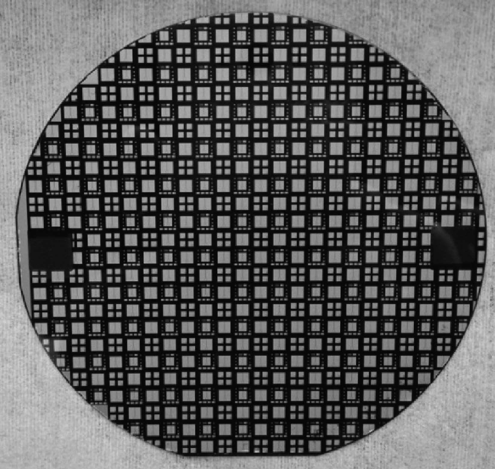
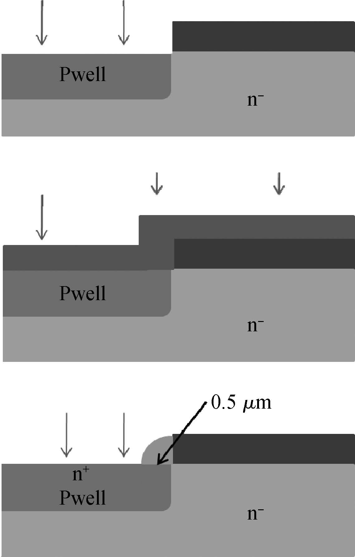
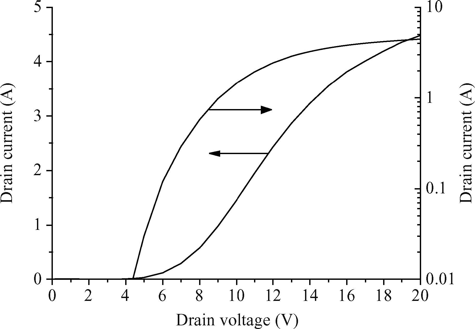
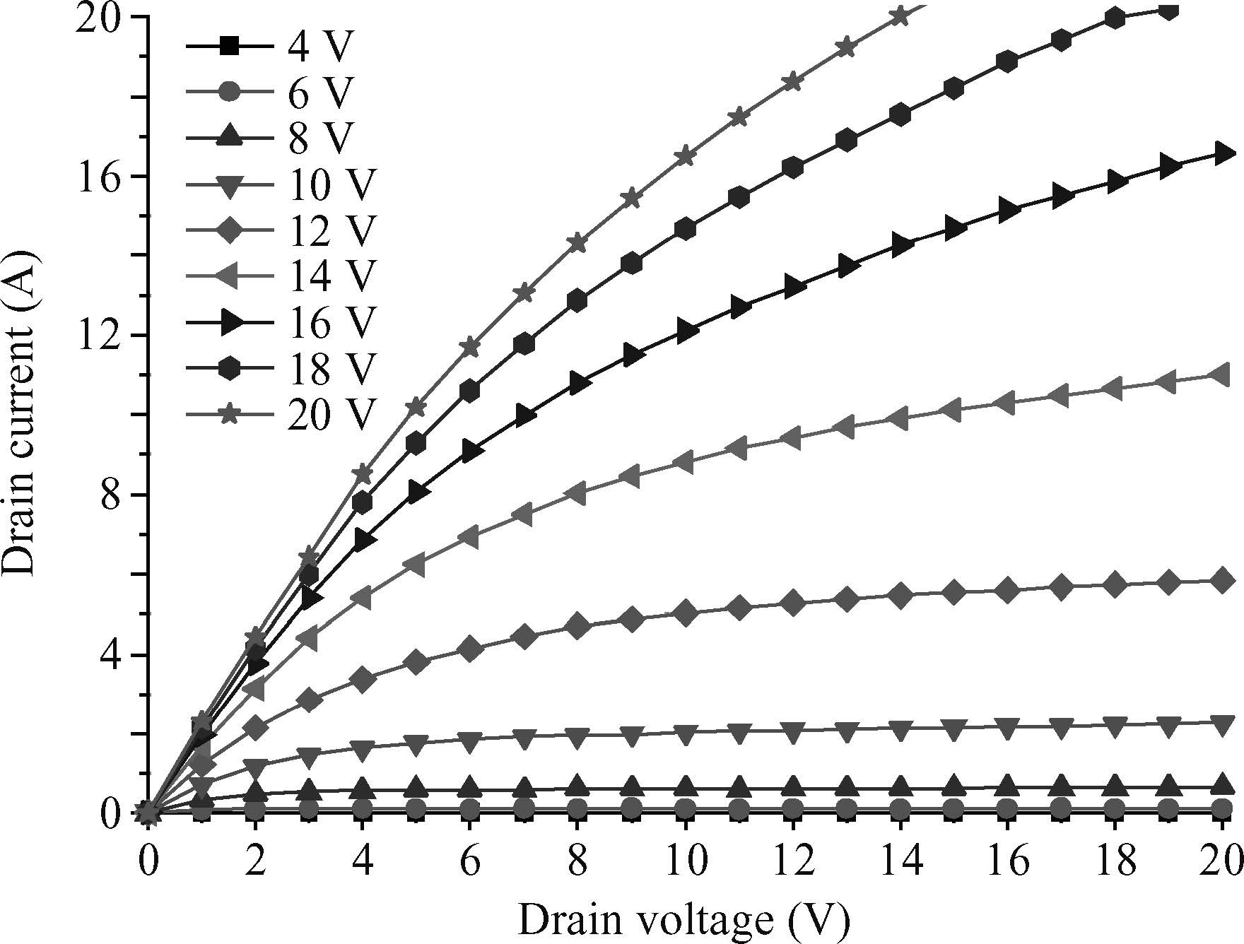
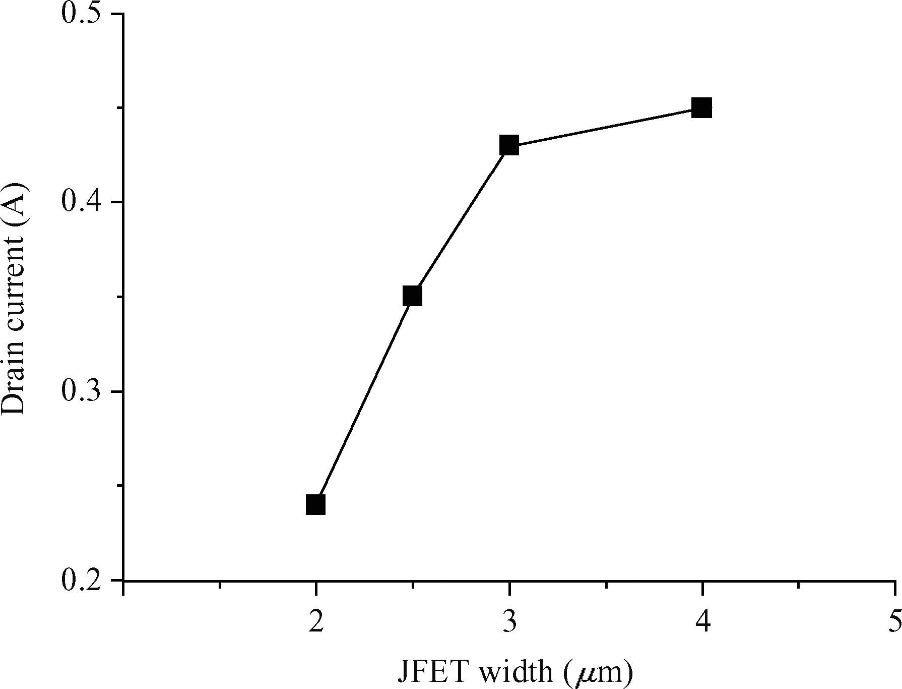
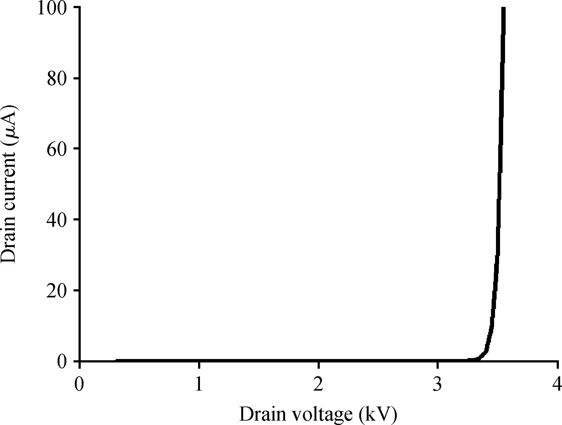
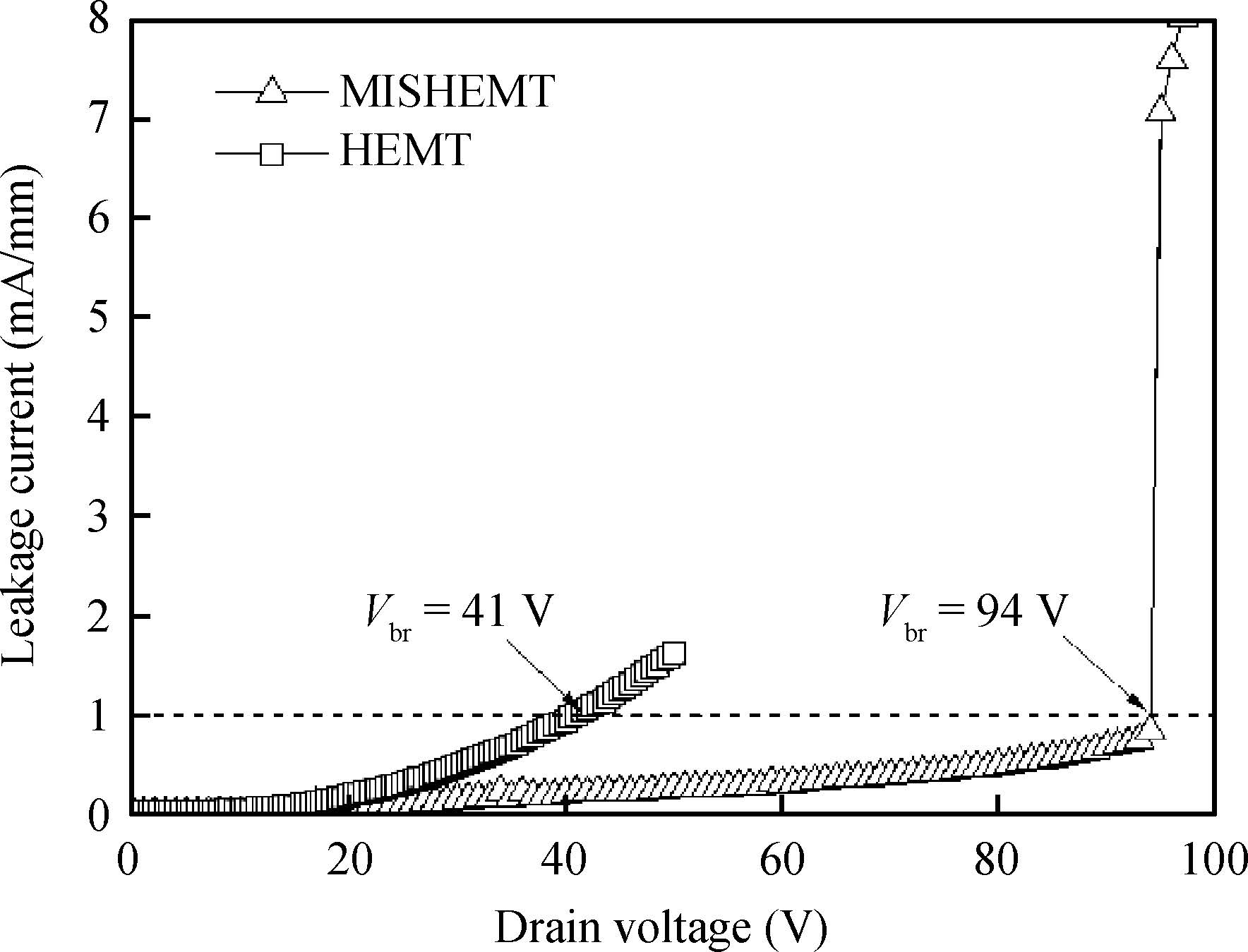
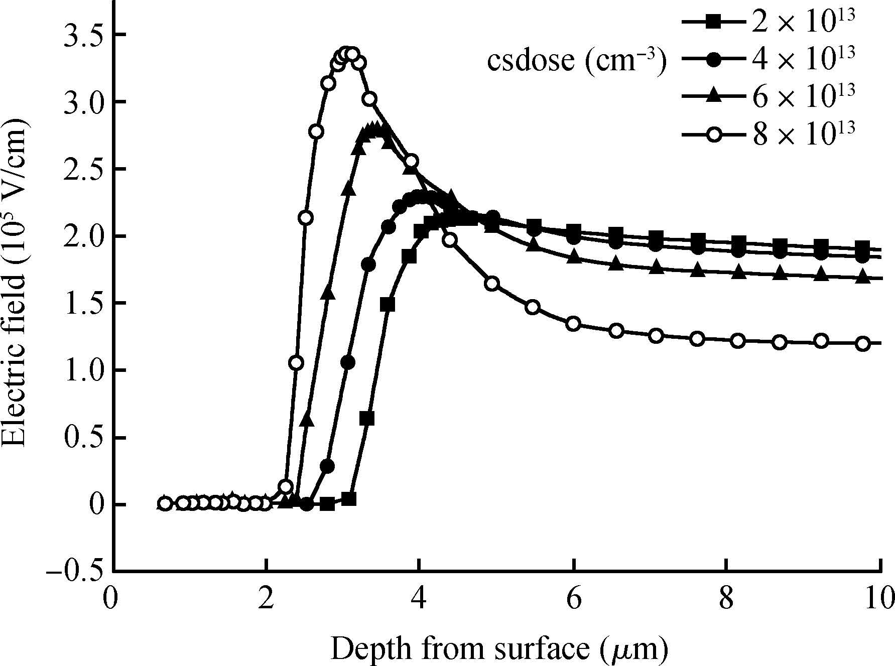
A 4H-SiC MOSFET with breakdown voltage higher than 3300 V has been successfully designed and fabricated. Numerical simulations have been performed to optimize the parameters of the drift layer and DMOSFET cell structure of active area. The n-type epilayer is 33μm thick with a doping of 2.5 × 1015 cm-3. The devices were fabricated with a floating guard ring edge termination. The drain current Id = 5 A at Vg = 20 V, corresponding to Vd = 2.5 V.
J. Semicond.
2015, 36(9): 094003 doi: 10.1088/1674-4926/36/9/094003

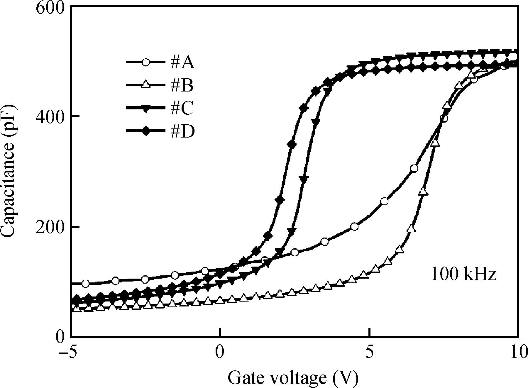
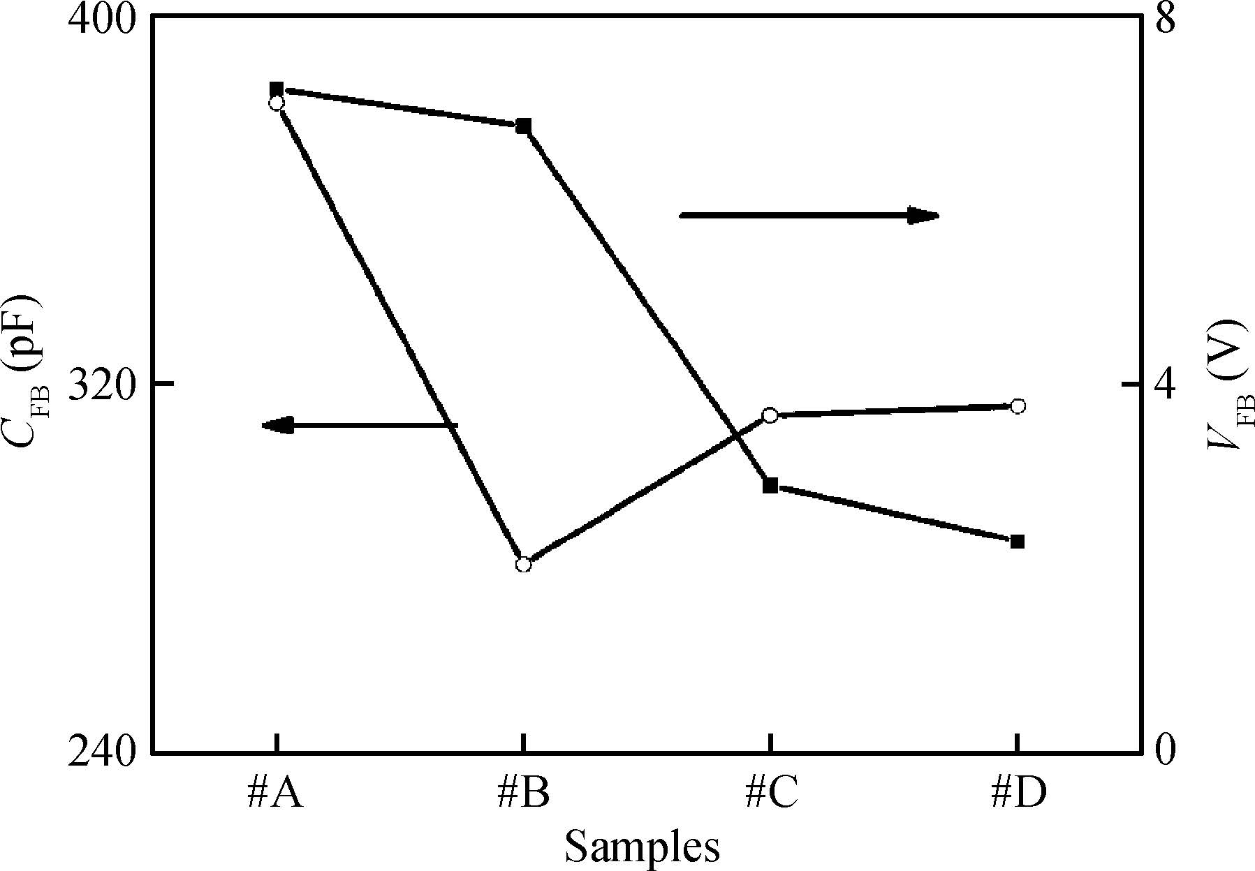
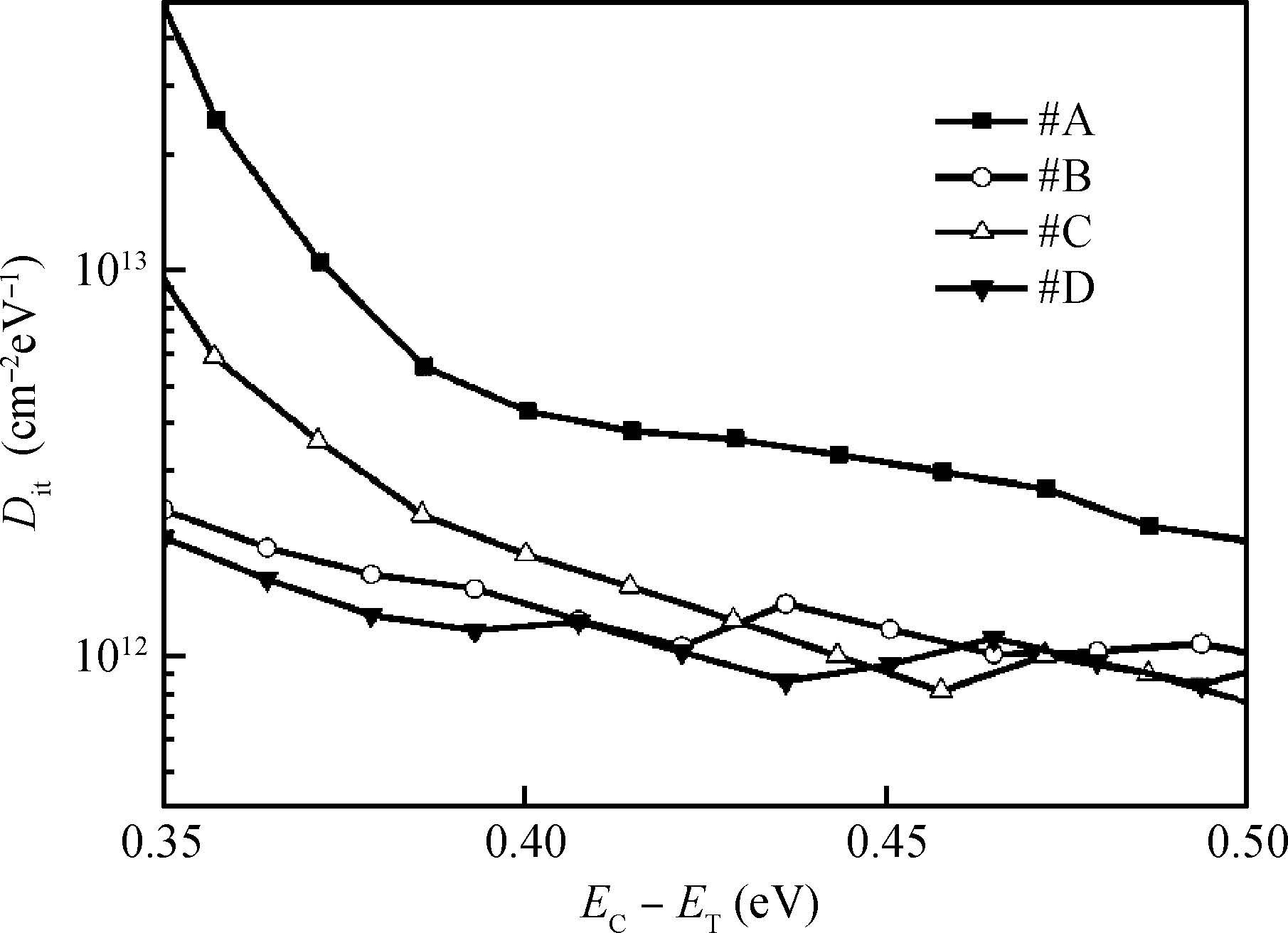
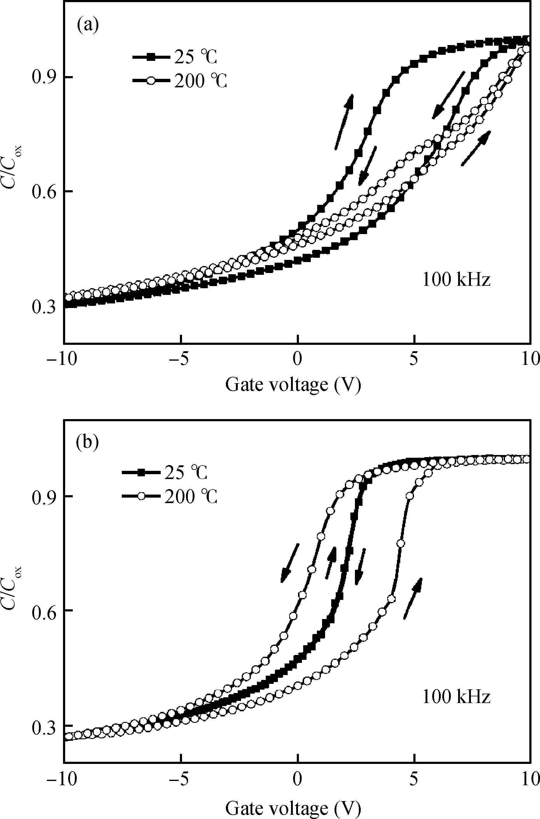
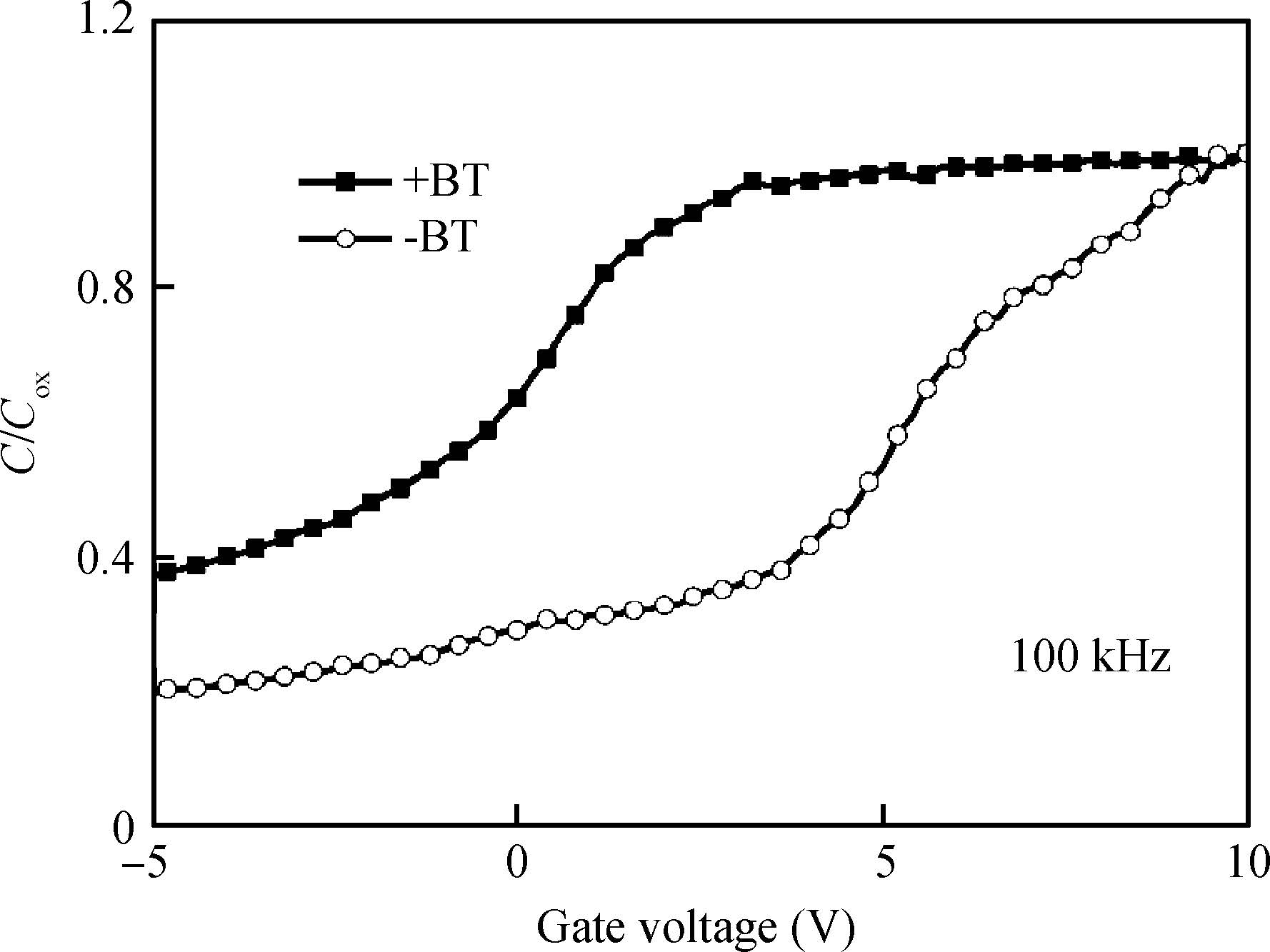
The interface properties of 4H-SiC metal-oxide-semiconductor (MOS) capacitors with post-oxidation annealing (POA) in nitric oxide (NO) ambient after high temperature (1300 ℃) oxidation have been investigated using capacitance-voltage (C-V) measurements. The experimental results show that the interface states density can be obviously decreased by the POA in NO ambient, and further reduced with increasing POA temperature and time. In the meantime interface state density and oxidation time could be lowered at higher thermal oxidation temperature, which results in the better oxide MOS characteristics and lower production costs. POA temperature and time dependence of 4H-SiC MOS interface are also discussed in detail.
J. Semicond.
2015, 36(9): 094004 doi: 10.1088/1674-4926/36/9/094004

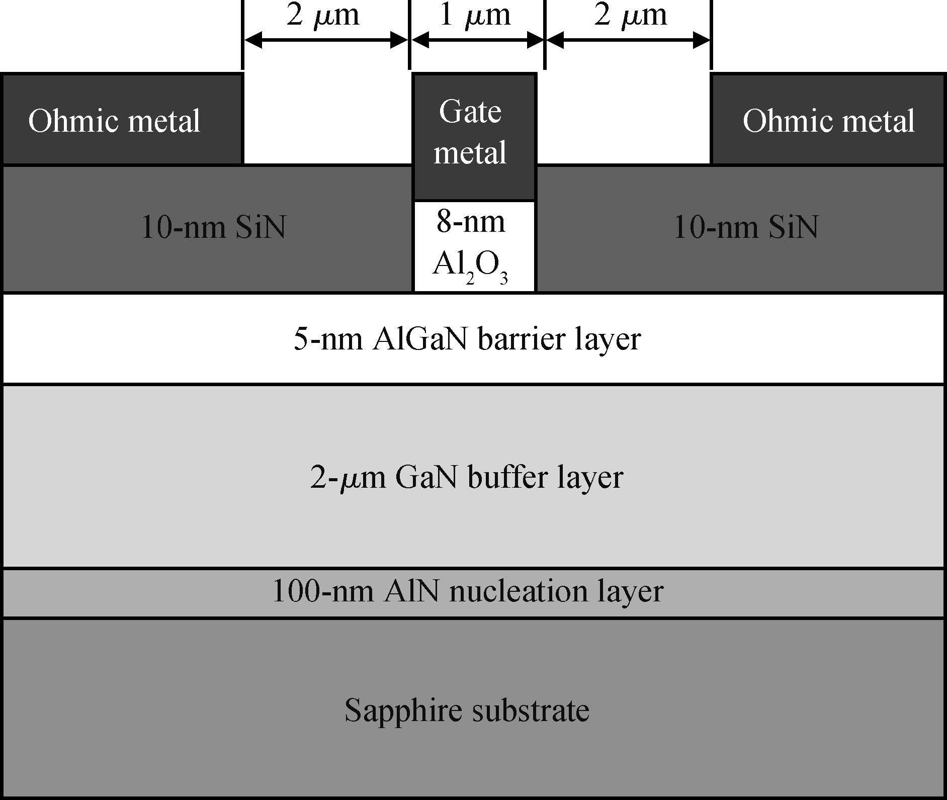
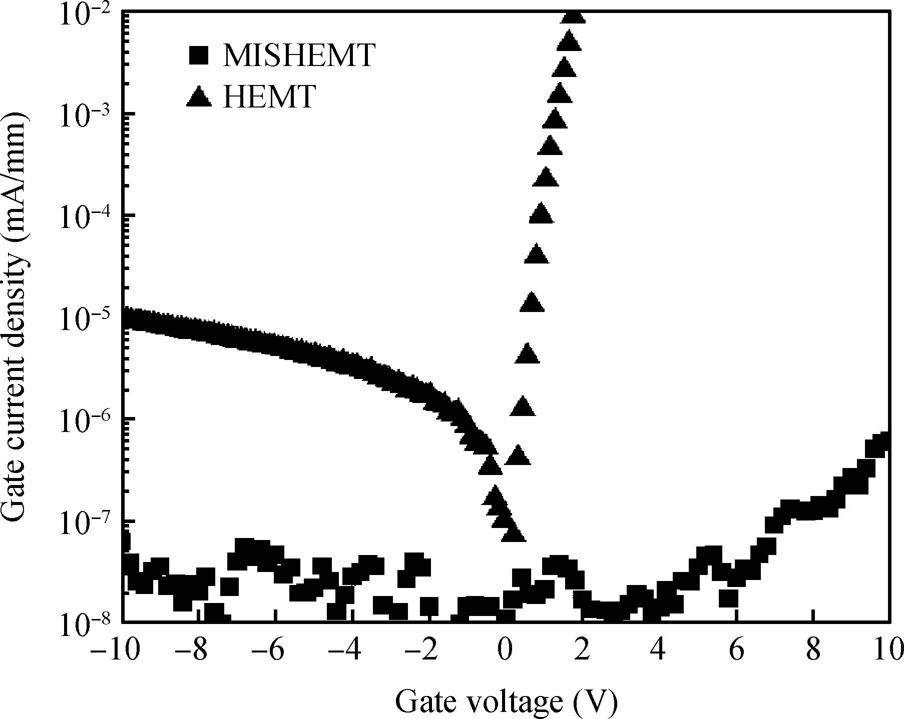
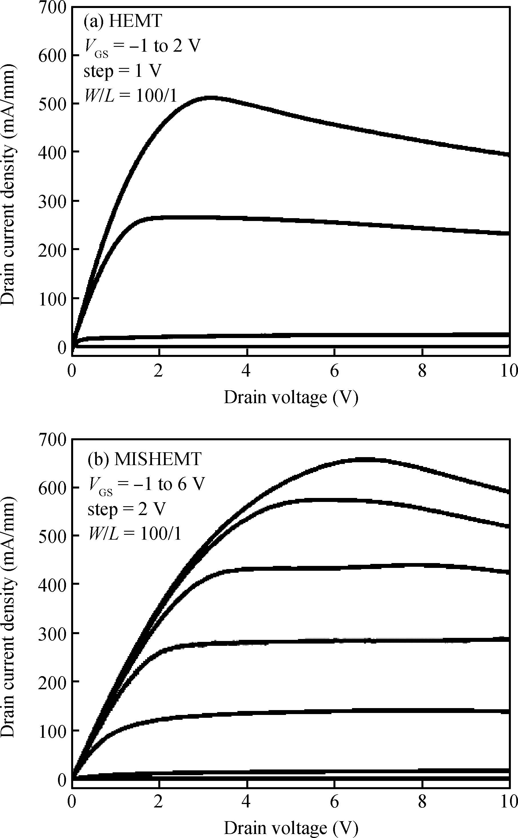
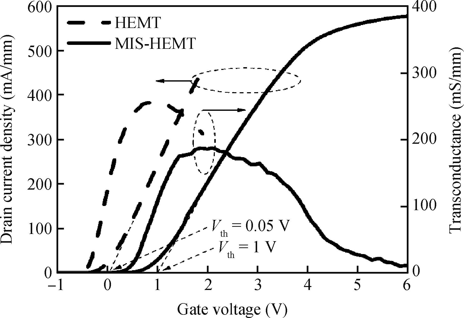
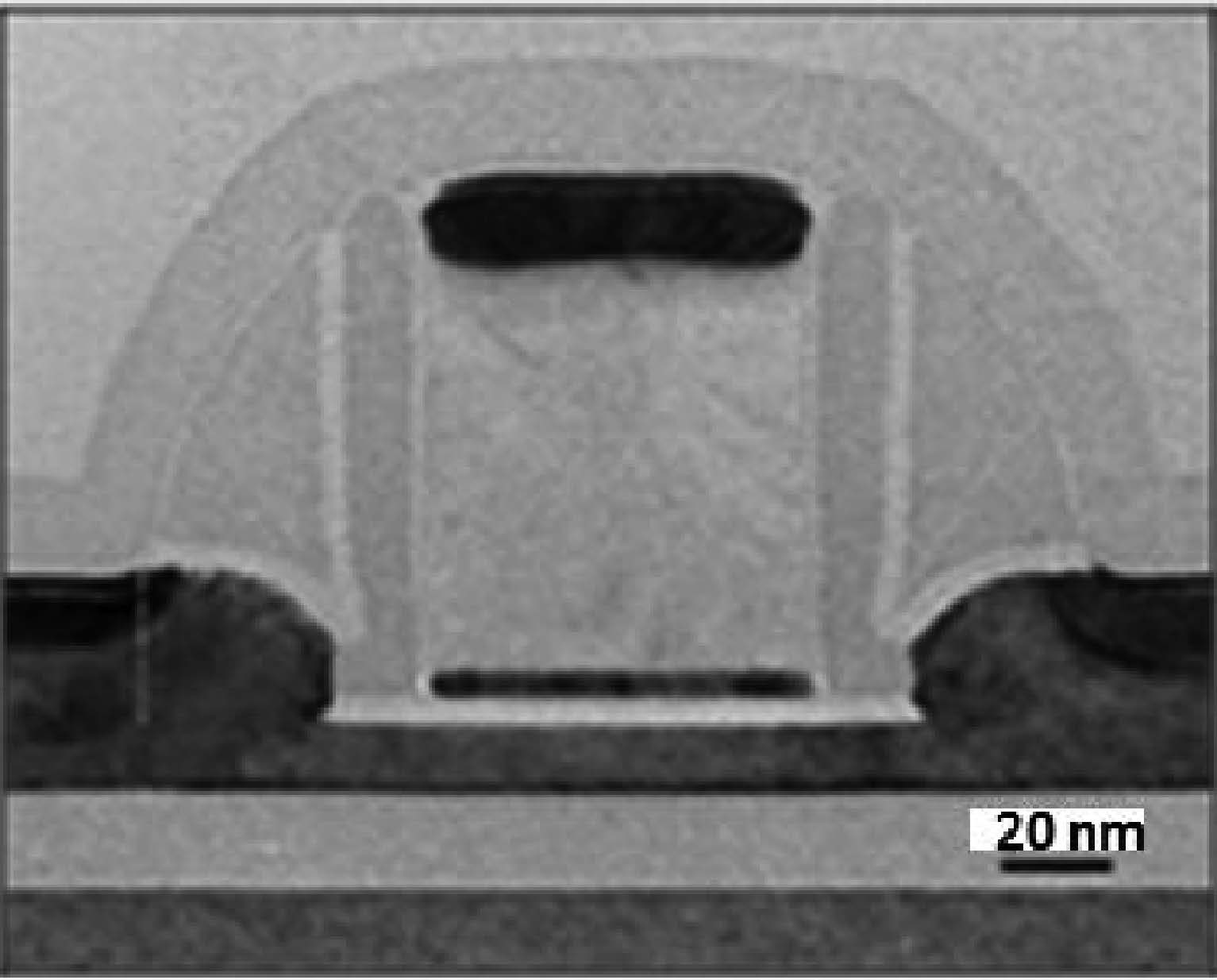
A high-performance enhancement-mode (E-mode) gallium nitride (GaN)-based metal-insulator-semiconductor high electron mobility transistor (MIS-HEMT) that employs a 5-nm-thick aluminum gallium nitride (Al0.3Ga0.7N) as a barrier layer and relies on silicon nitride (SiN) passivation to control the 2DEG density is presented. Unlike the SiN passivation, aluminum oxide (Al2O3) by atomic layer deposition (ALD) on AlGaN surface would not increase the 2DEG density in the heterointerface. ALD Al2O3 was used as gate insulator after the depletion by etching of the SiN in the gate region. The E-mode MIS-HEMT with gate length (LG) of 1μm showed a maximum drain current density (IDS) of 657 mA/mm, a maximum extrinsic transconductance (gm) of 187 mS/mm and a threshold voltage (Vth) of 1 V. Comparing with the corresponding E-mode HEMT, the device performances had been greatly improved due to the insertion of Al2O3 gate insulator. This provided an excellent way to realize E-mode AlGaN/GaN MIS-HEMTs with both high Vth and IDS.
J. Semicond.
2015, 36(9): 094005 doi: 10.1088/1674-4926/36/9/094005

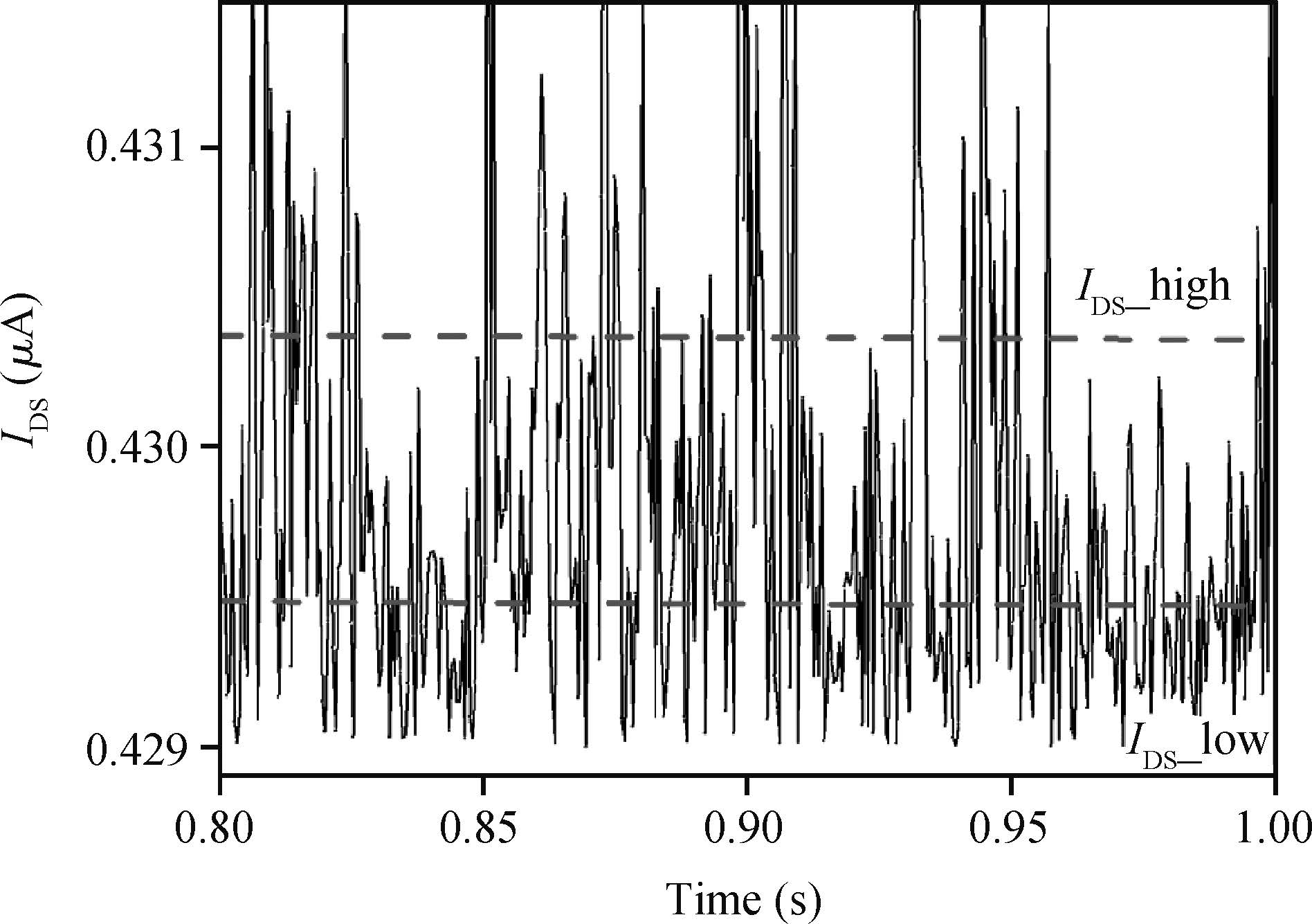
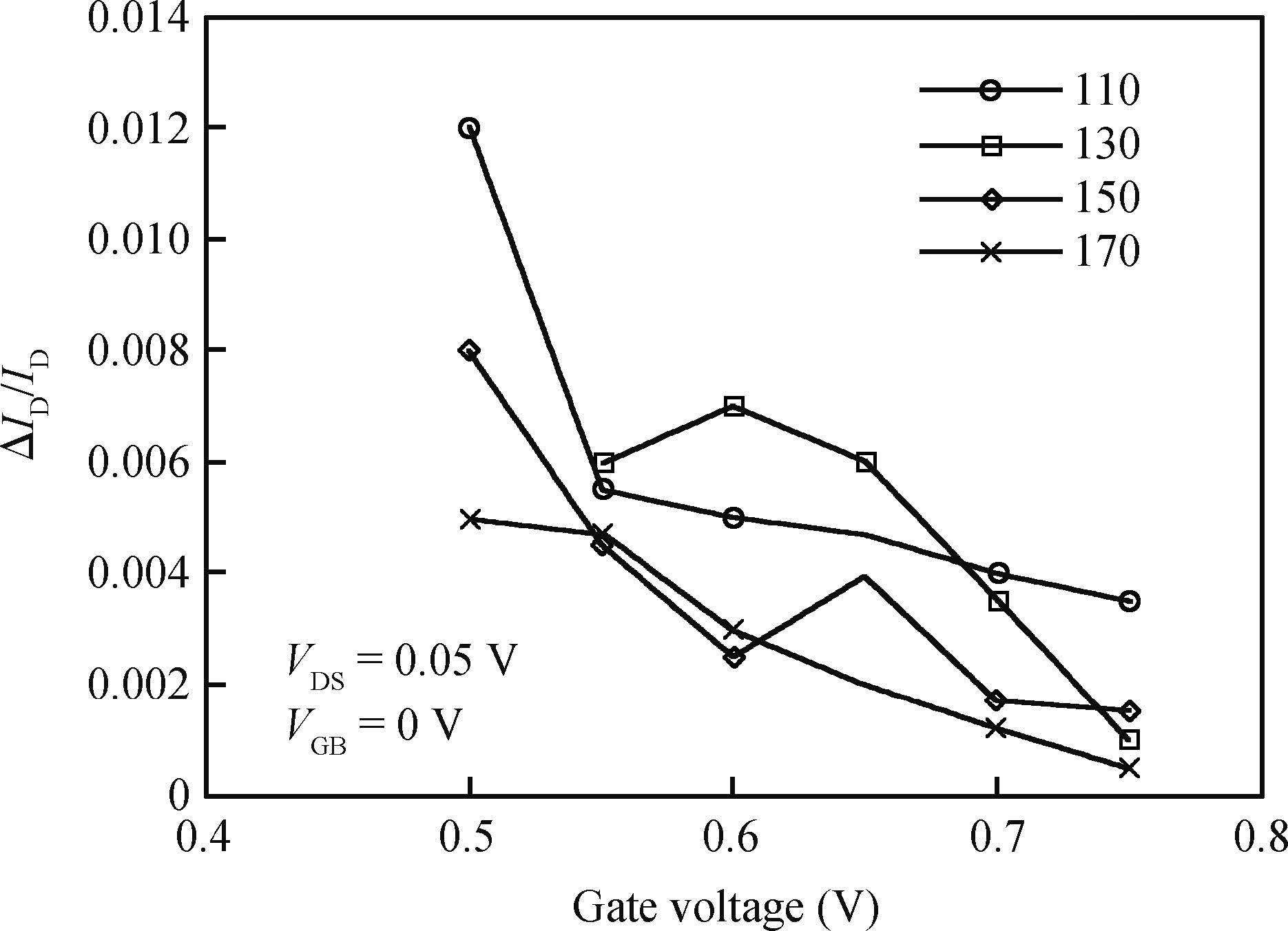
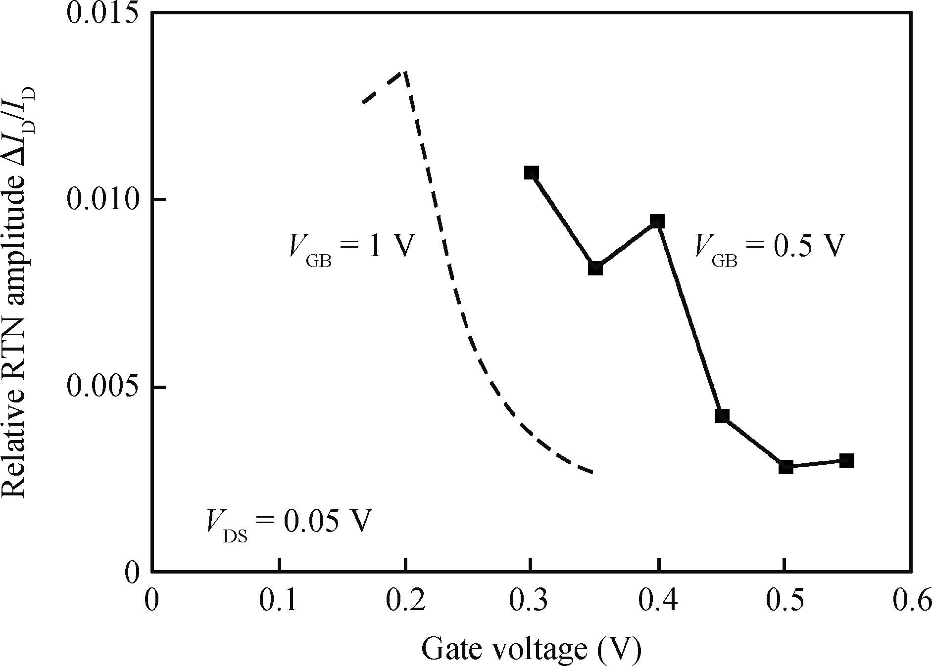
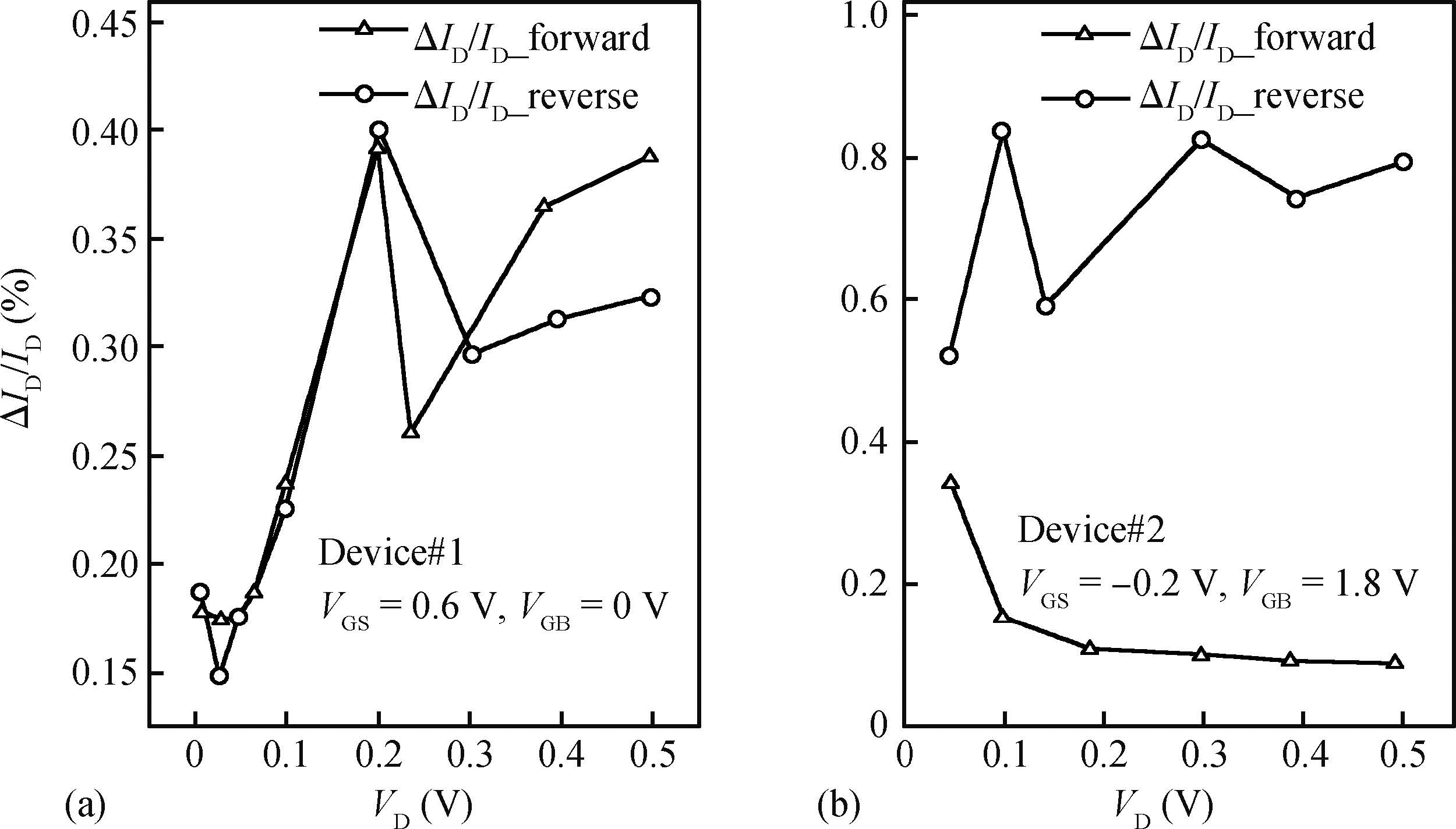
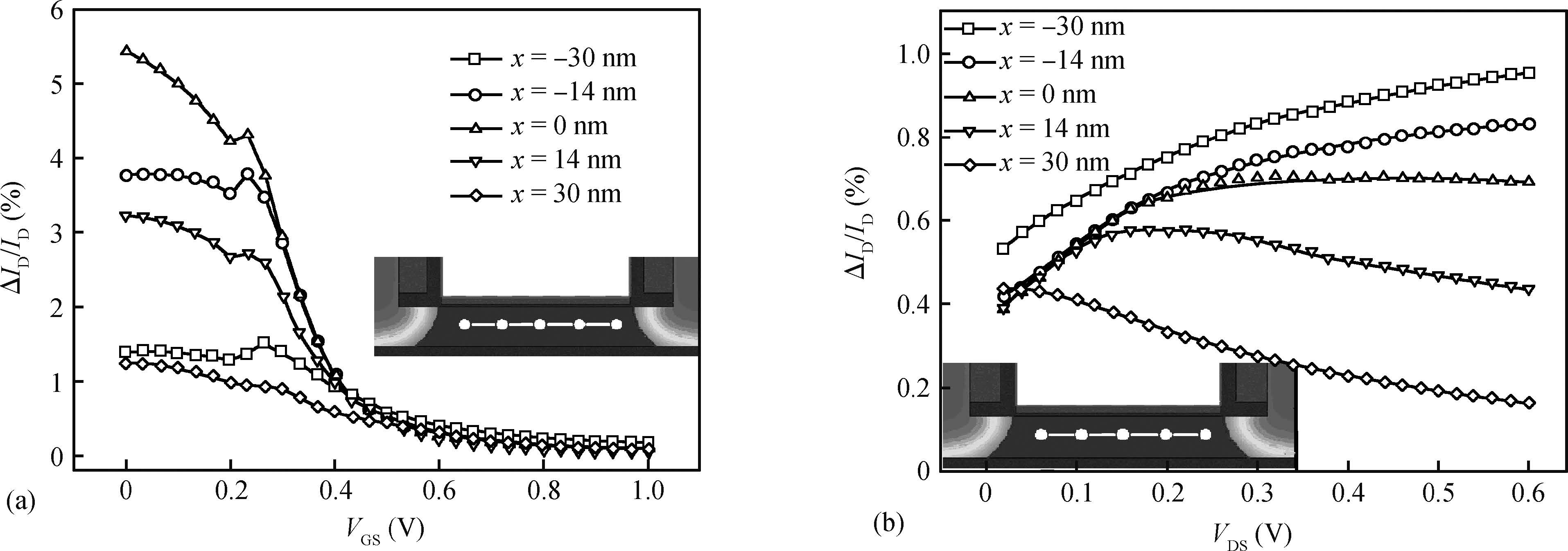
This paper studies the amplitude of random telegraph noise (RTN) caused by a single trap in the silicon film of ultra-thin buried oxide (UTBOX) silicon-on-insulator (SOI) devices. The film-defect-related RTN was identified and analyzed by low frequency noise measurement and time domain measurement. Emphasis is on the relative amplitude ΔID/ID, which is studied in the function of the front-gate, the back-gate and the drain-to-source biases. Interesting asymmetric or symmetric VDS dependence of switched source and drain are observed and supported by calibrated Sentaurus simulations. It is believed the asymmetry of the VDS dependence of the switched source and drain is related to the lateral trap position along the source and drain.
J. Semicond.
2015, 36(9): 094006 doi: 10.1088/1674-4926/36/9/094006

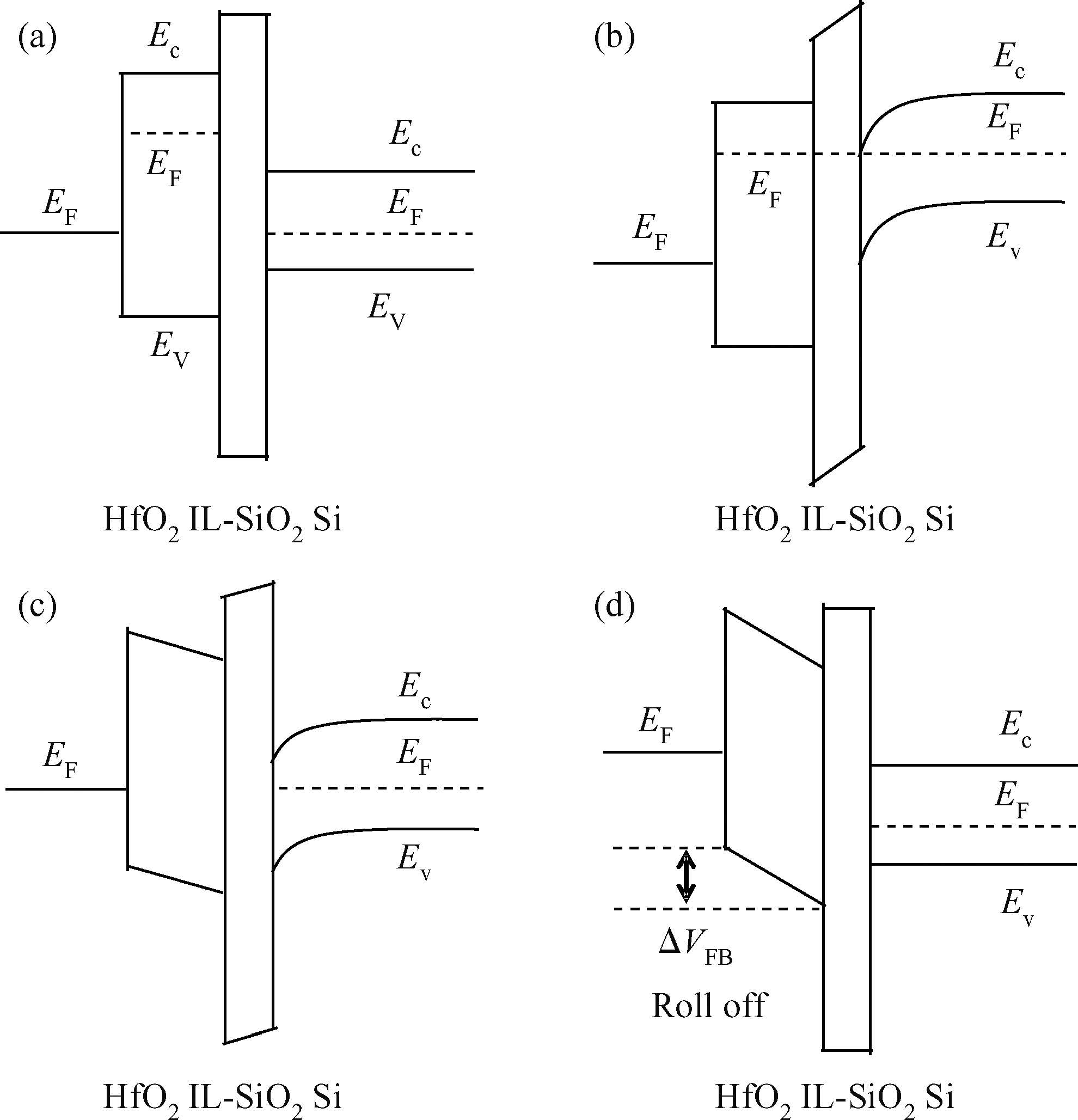
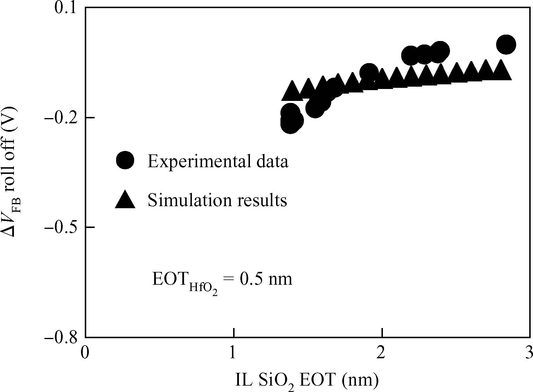
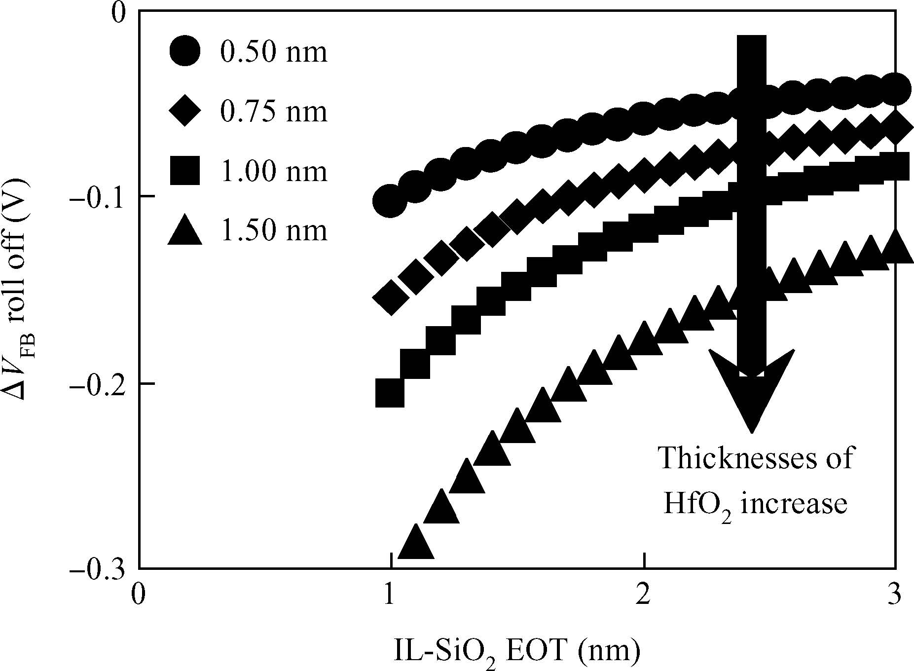
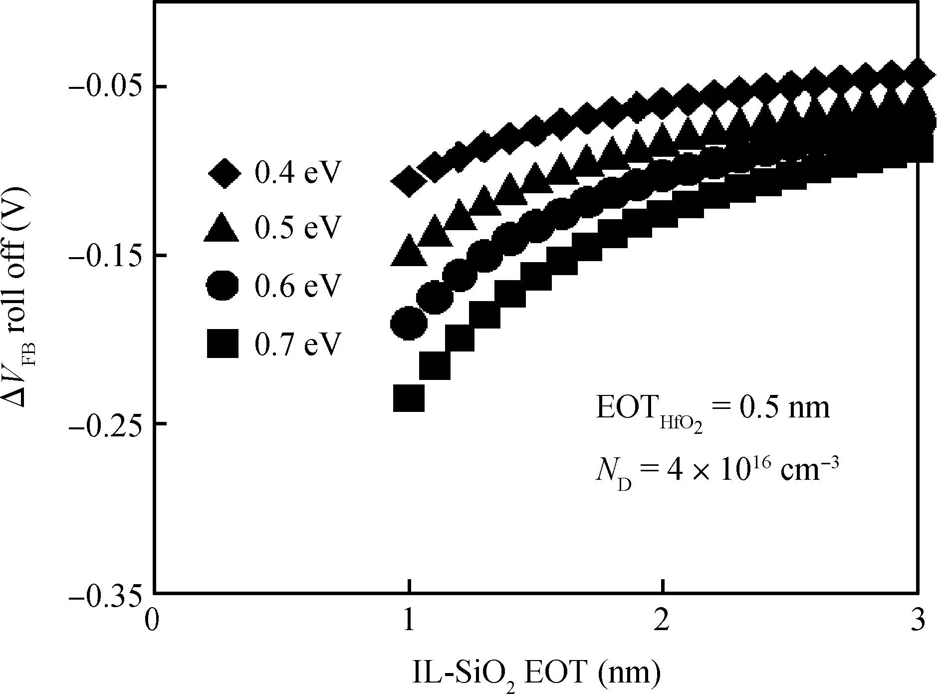
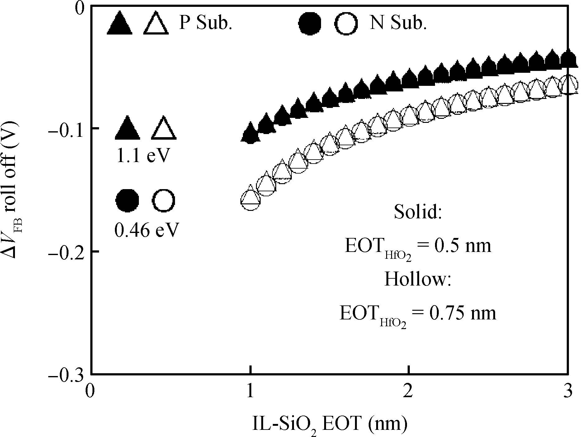
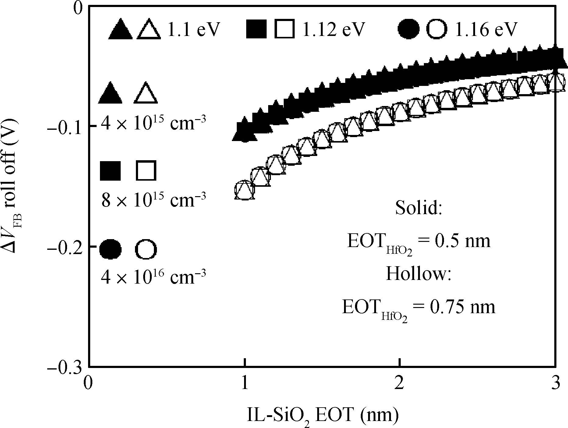
The physical origin of the flatband voltage (VFB) roll off for a metal-oxide-semiconductor device with high-k/metal gate structure is studied from the viewpoint of energy band alignment at the high-k/Si interface because the thickness of SiO2 interlayer is thin enough to be ignored. The VFB roll off phenomenon is assigned to associate with the direct electron transfer between high-k and Si substrate. Quantitatively calculated simulation results based on this model are given considering different conditions.
J. Semicond.
2015, 36(9): 094007 doi: 10.1088/1674-4926/36/9/094007

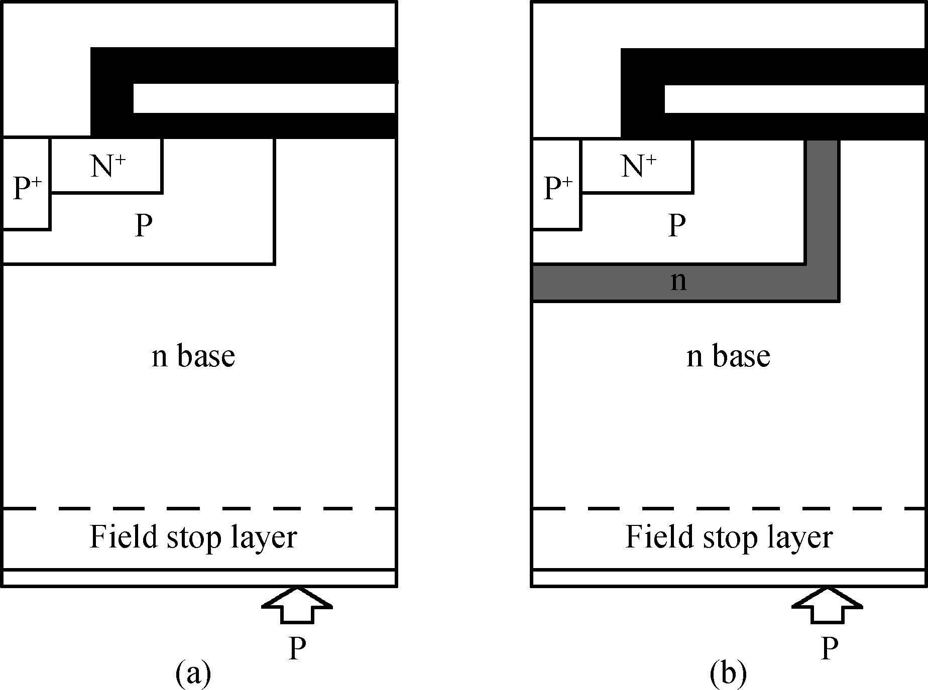
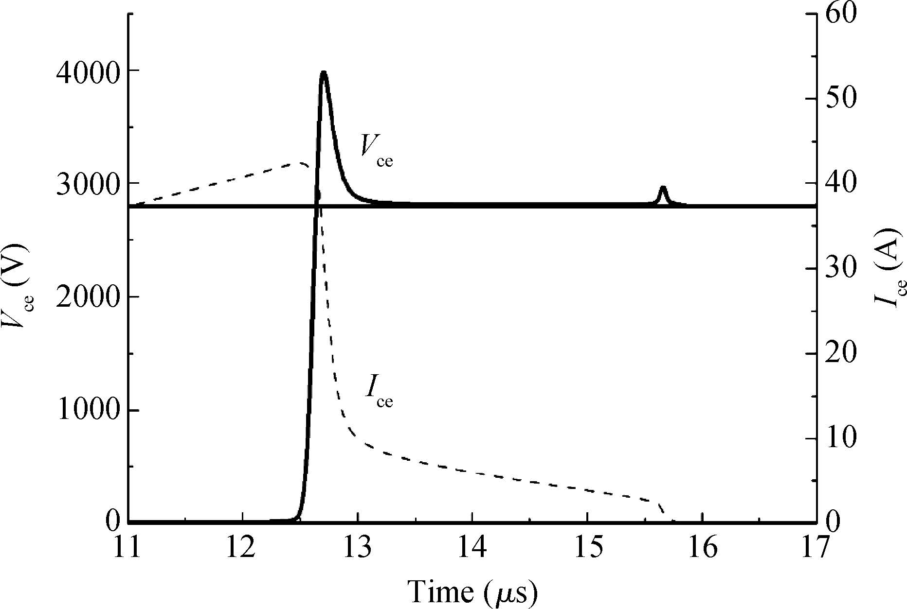
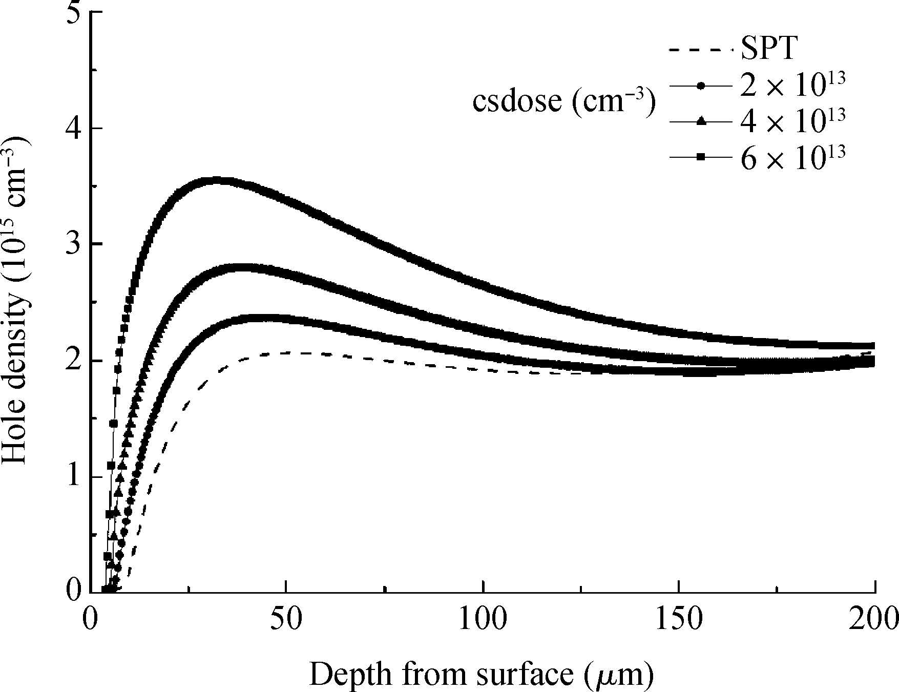
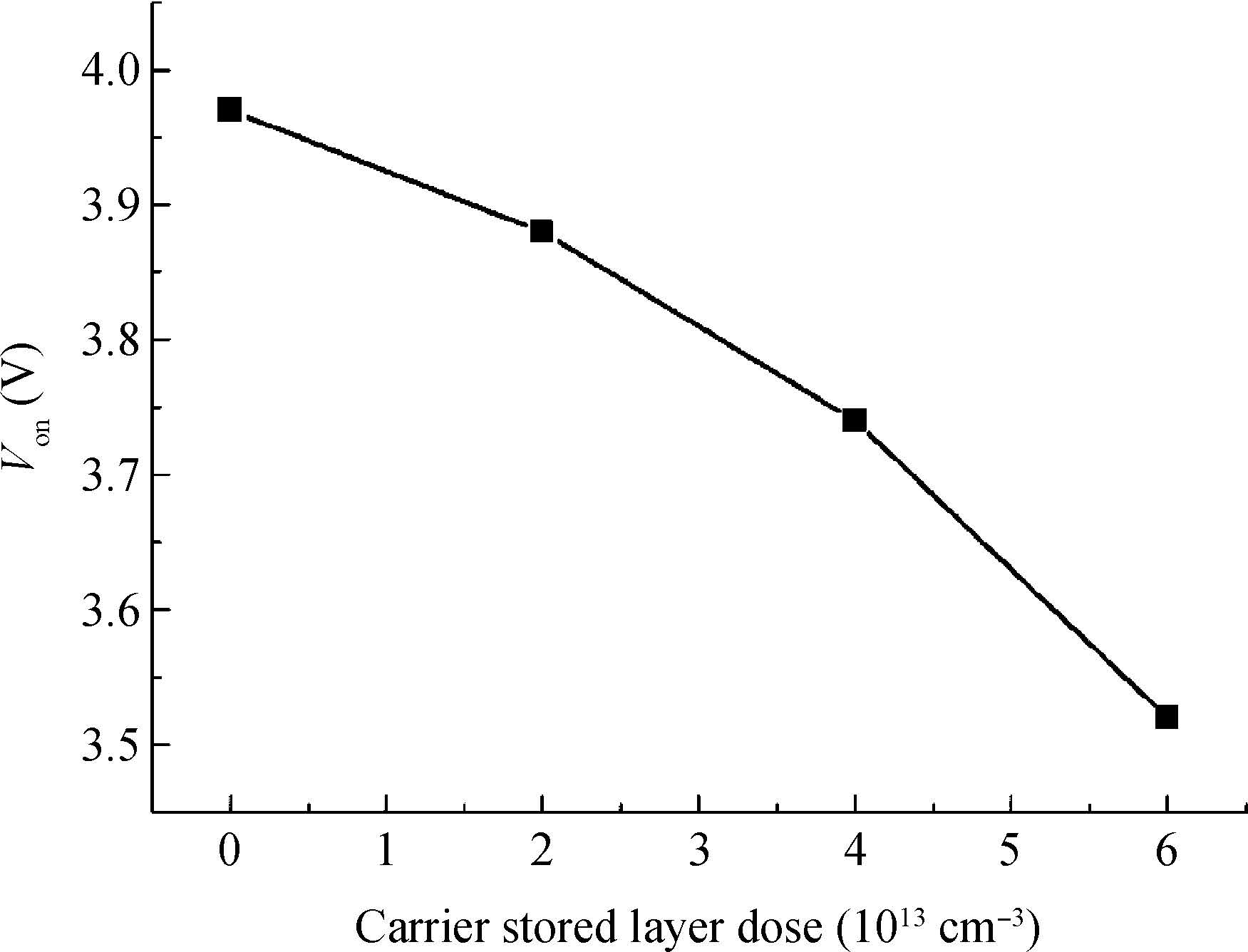
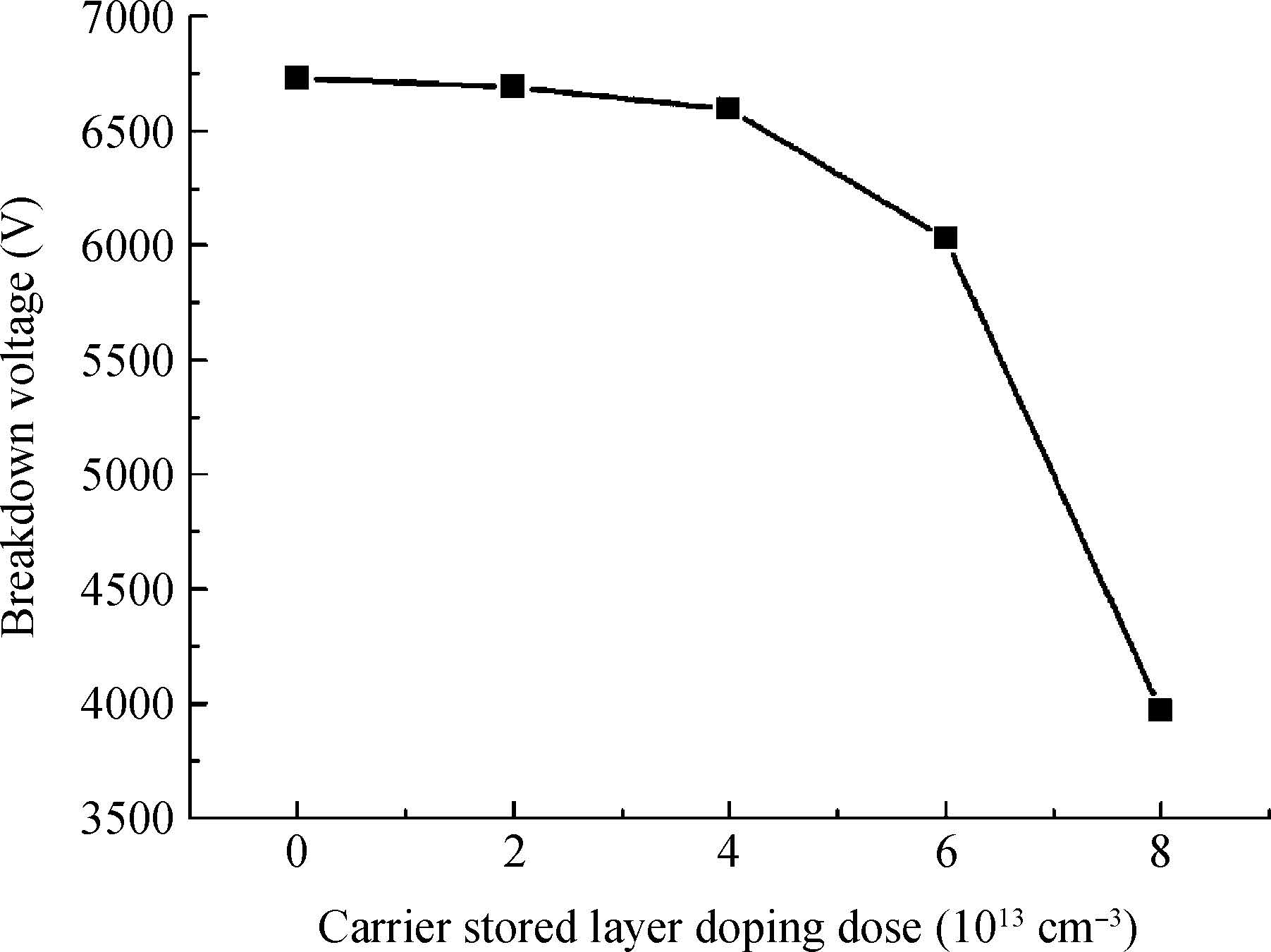
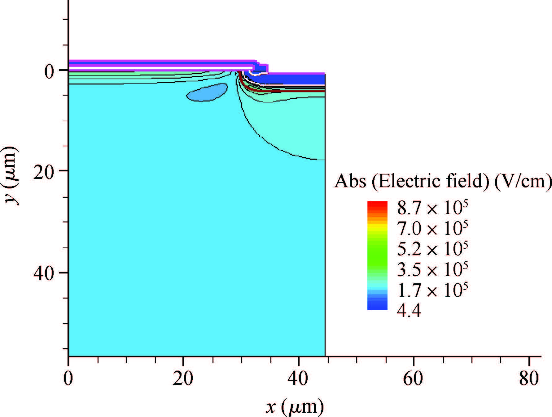
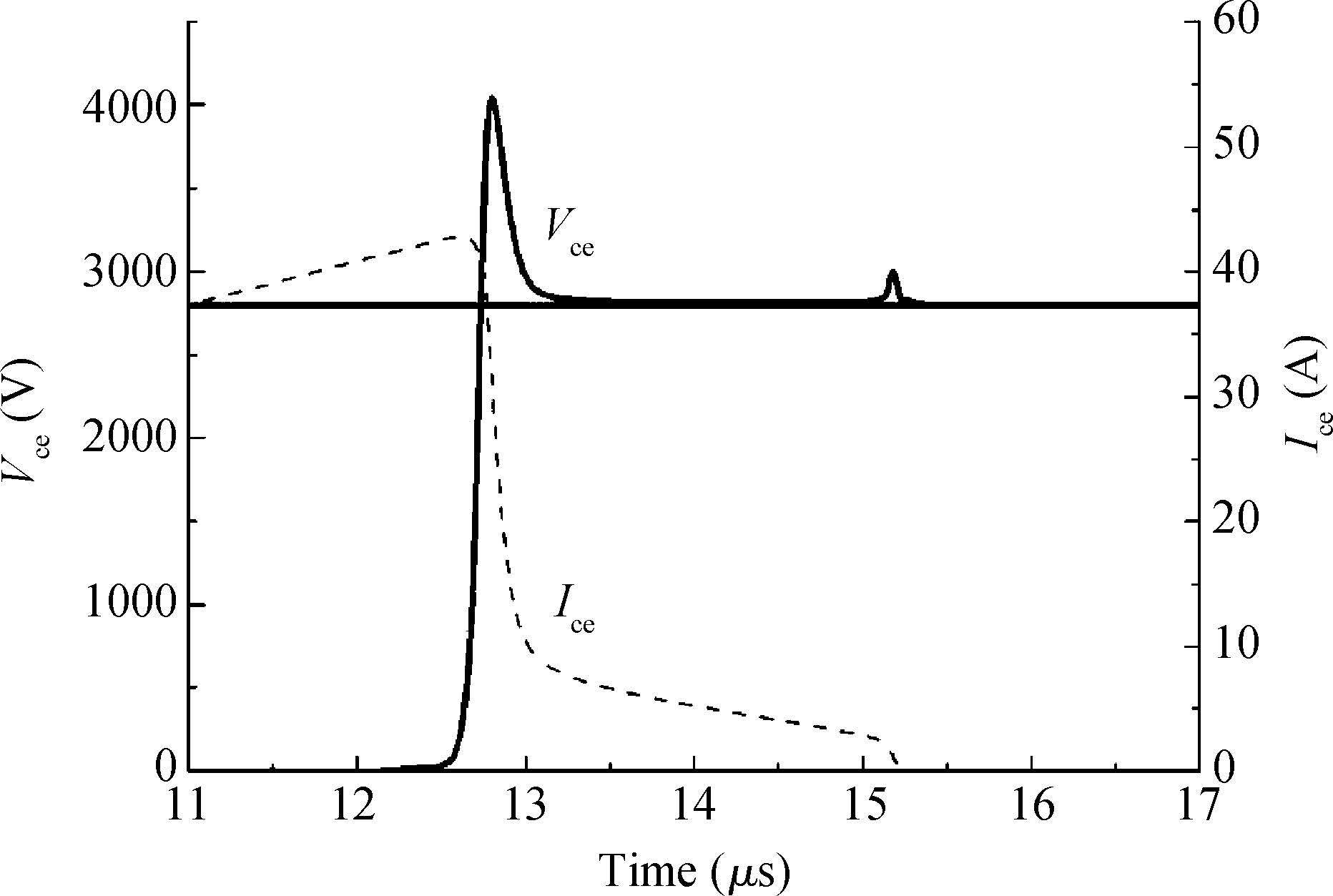
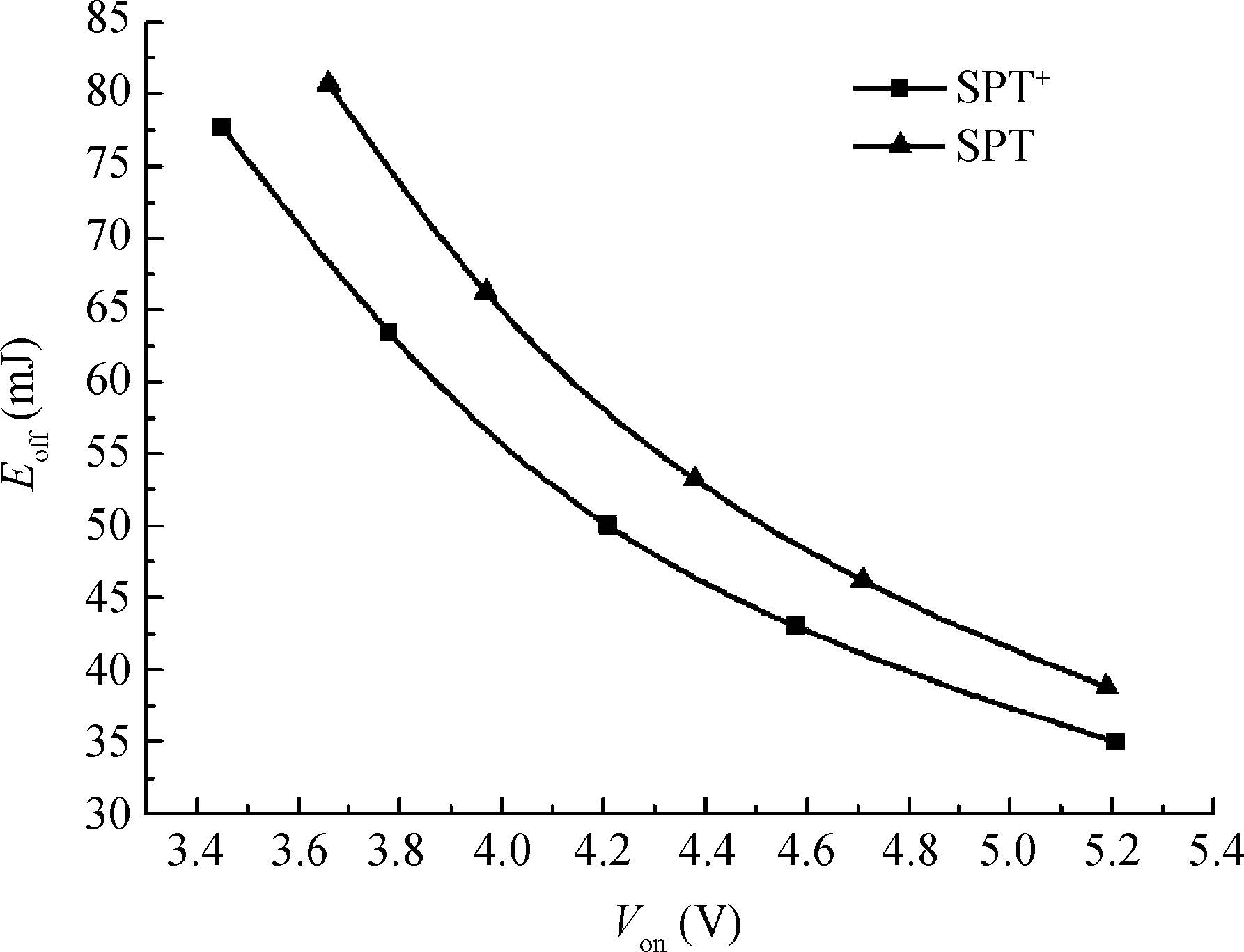
This paper concerns the need for improving the static and dynamic performance of the high voltage insulated gate bipolar transistor (HV IGBTs). A novel structure with a carrier stored layer on the cathode side, known as an enhanced planar IGBT of the 4500 V voltage class is investigated. With the adoption of a soft punch through (SPT) concept as the vertical structure and an enhanced planar concept as the top structure, signed as SPT+ IGBT, the simulation results indicate the turn-off switching waveform of the 4500 V SPT+ IGBT is soft and also realizes an improved trade-off relationship between on-state voltage drop (Von) and turn-off loss (Eoff) in comparison with the SPT IGBT. Attention is also paid to the influences caused by different carrier stored layer doping dose on static and dynamic performances, to optimize on-state and switching losses of SPT+ IGBT.

J. Semicond.
2015, 36(9): 094008 doi: 10.1088/1674-4926/36/9/094008

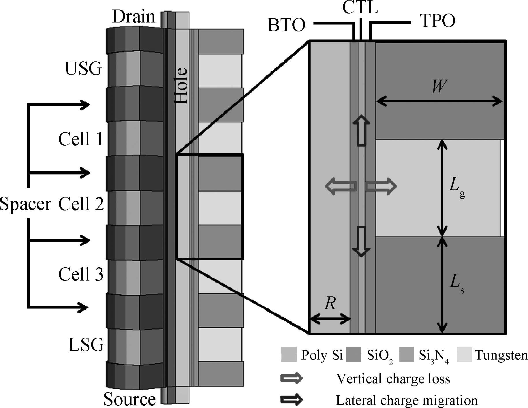
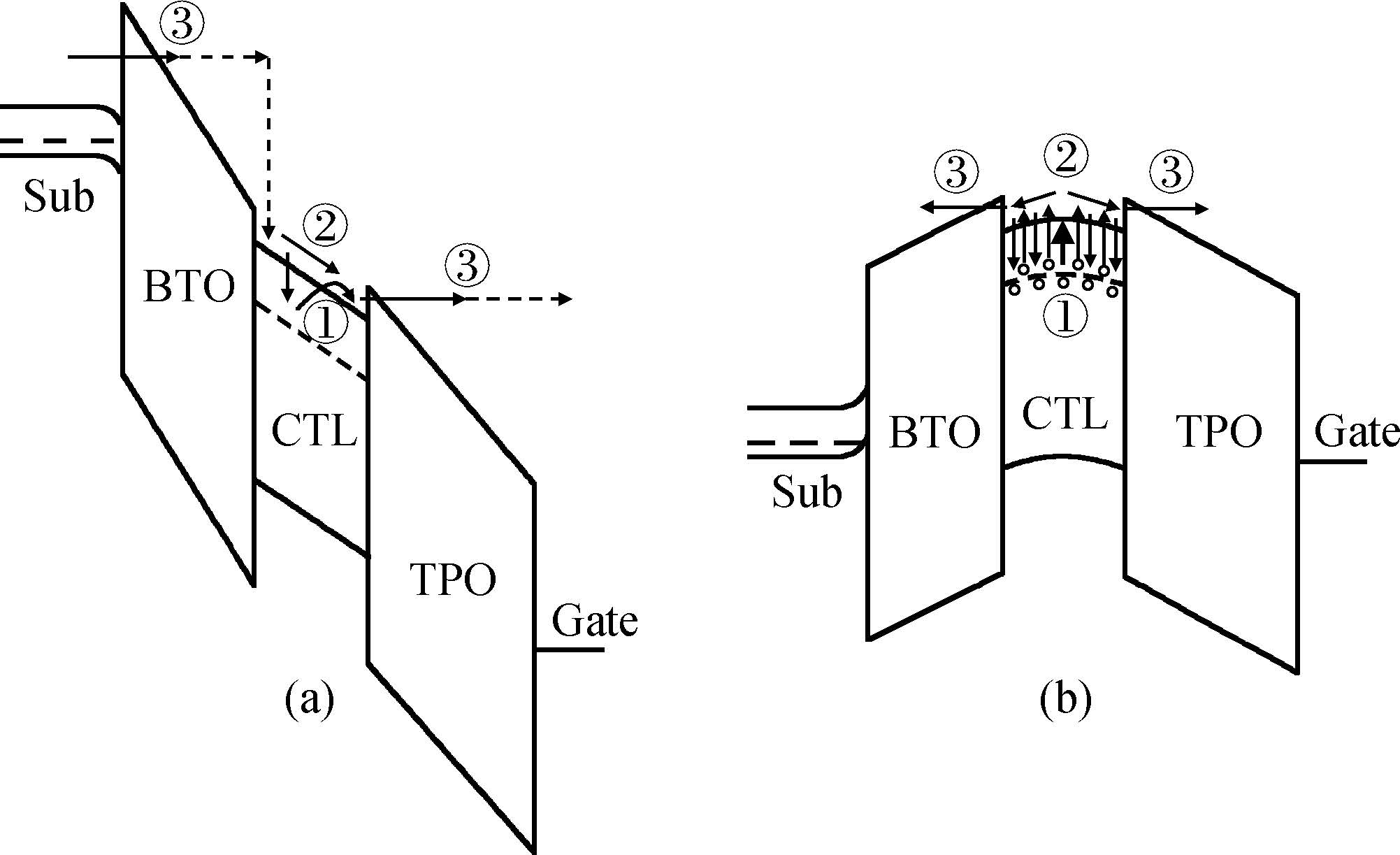
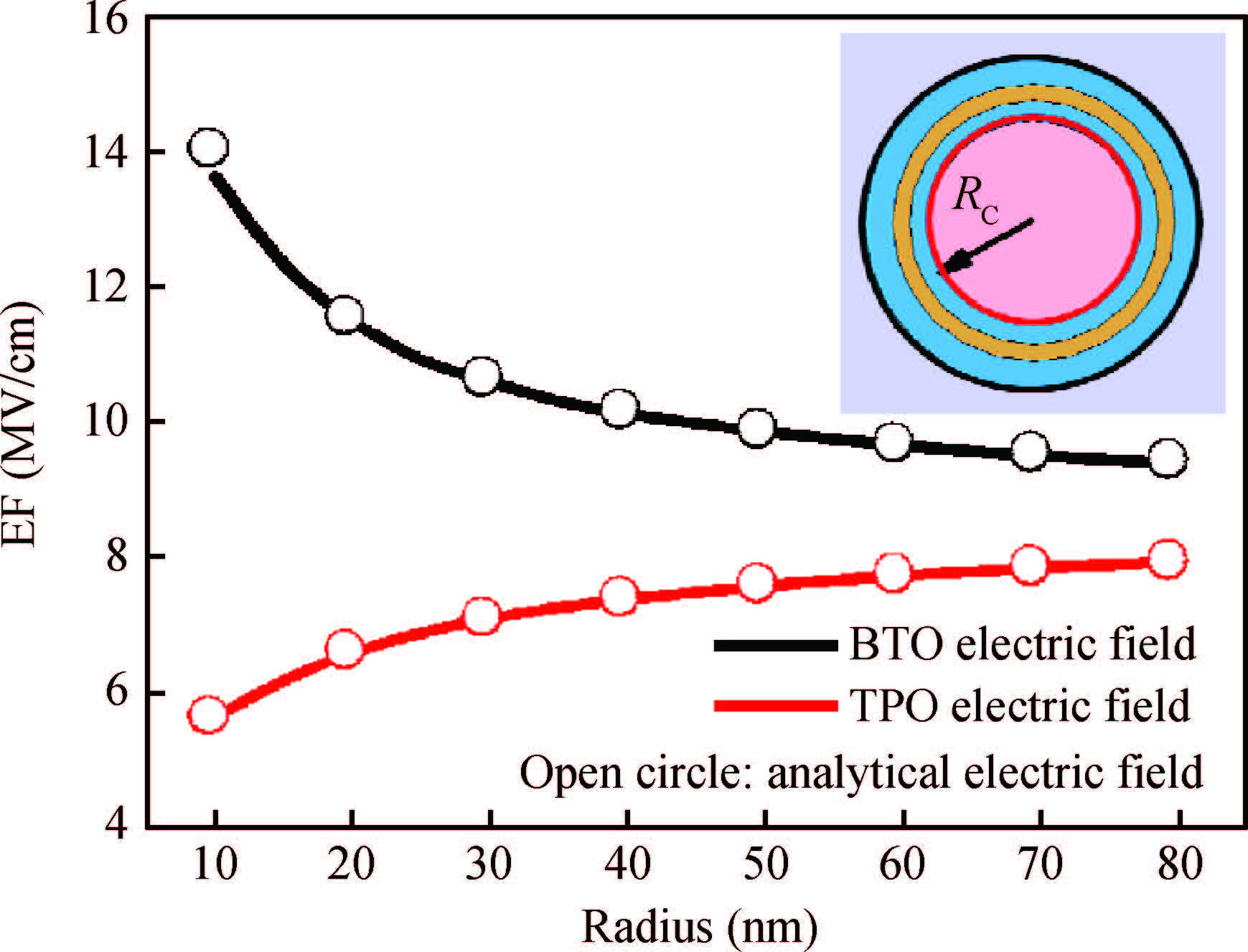
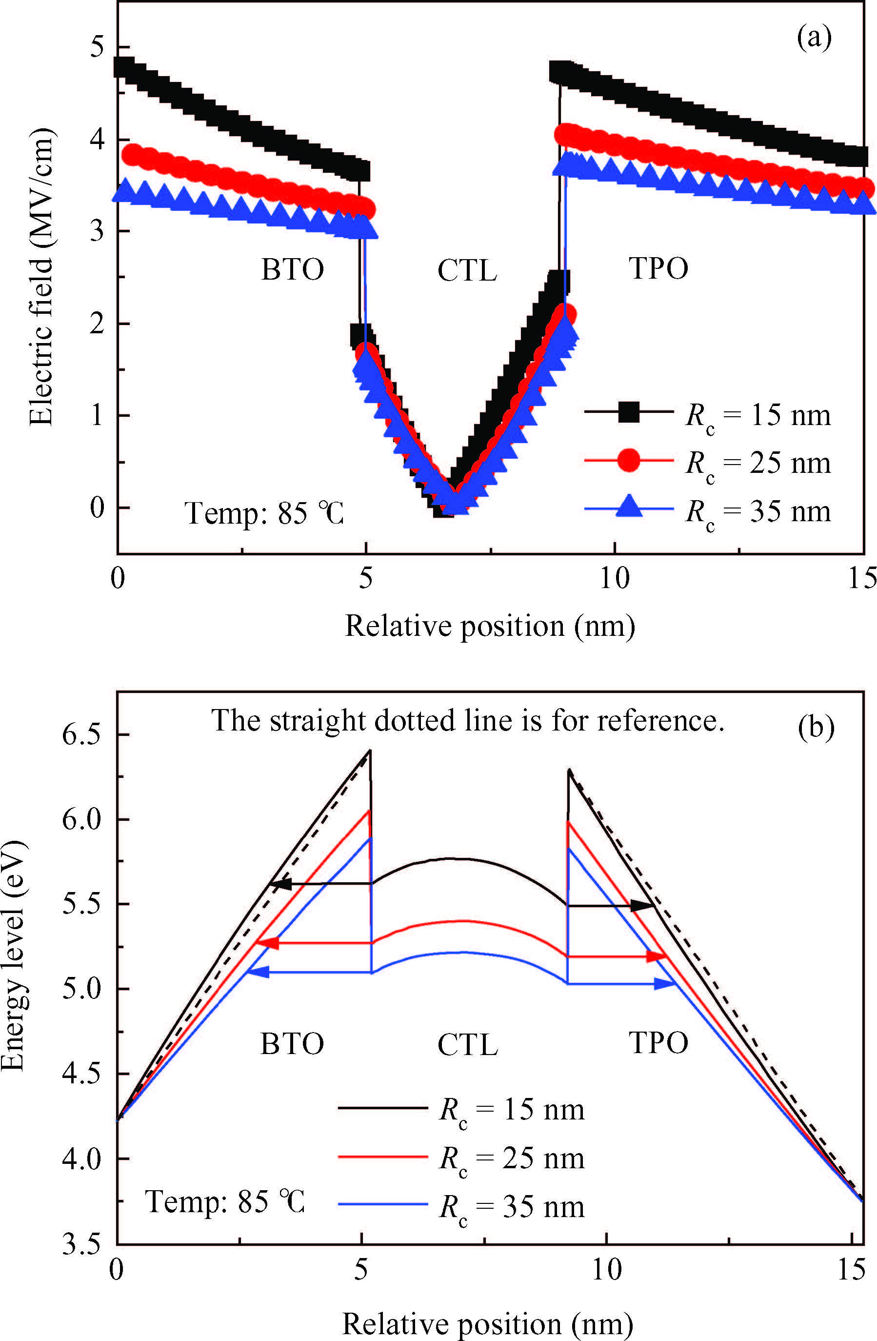
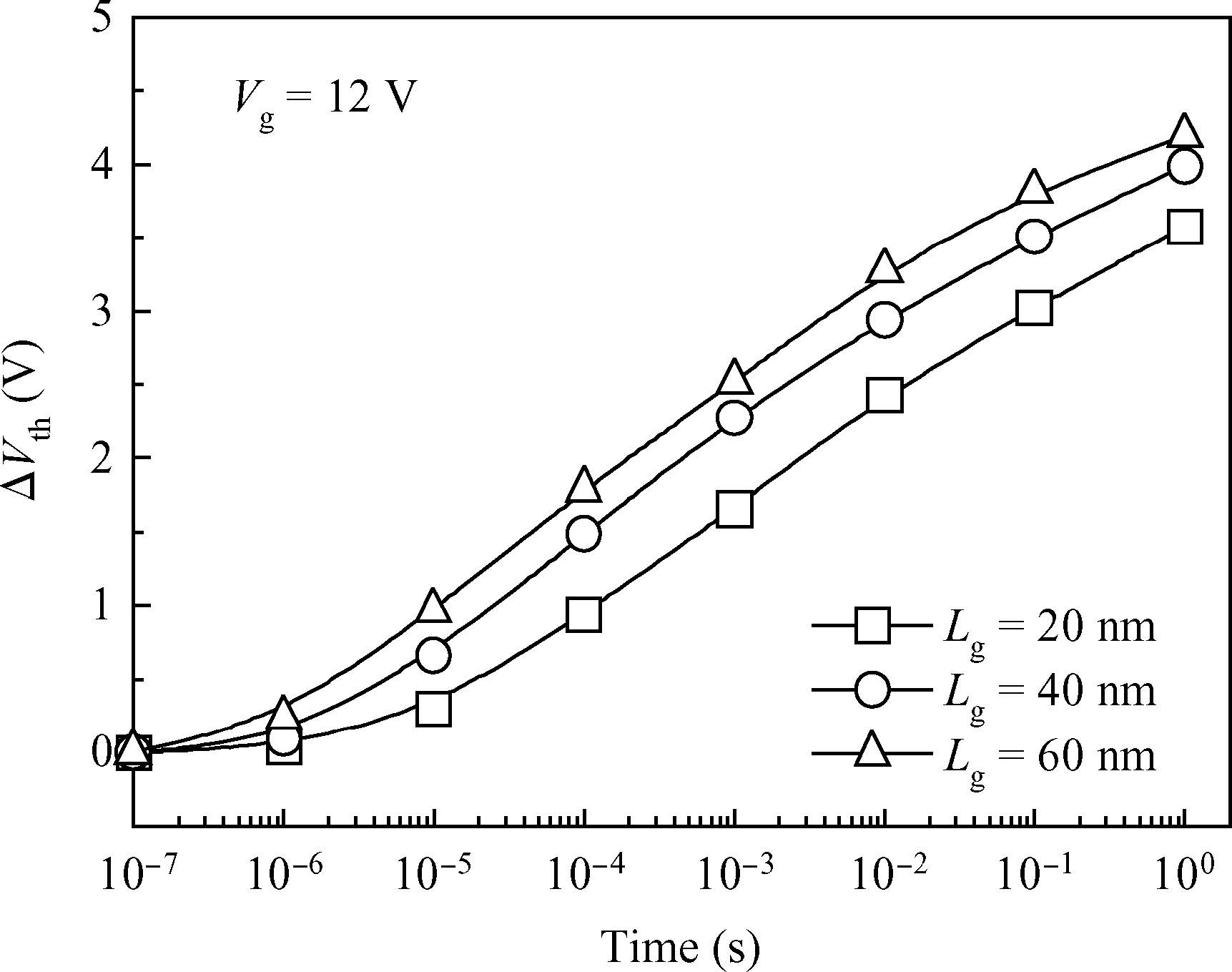
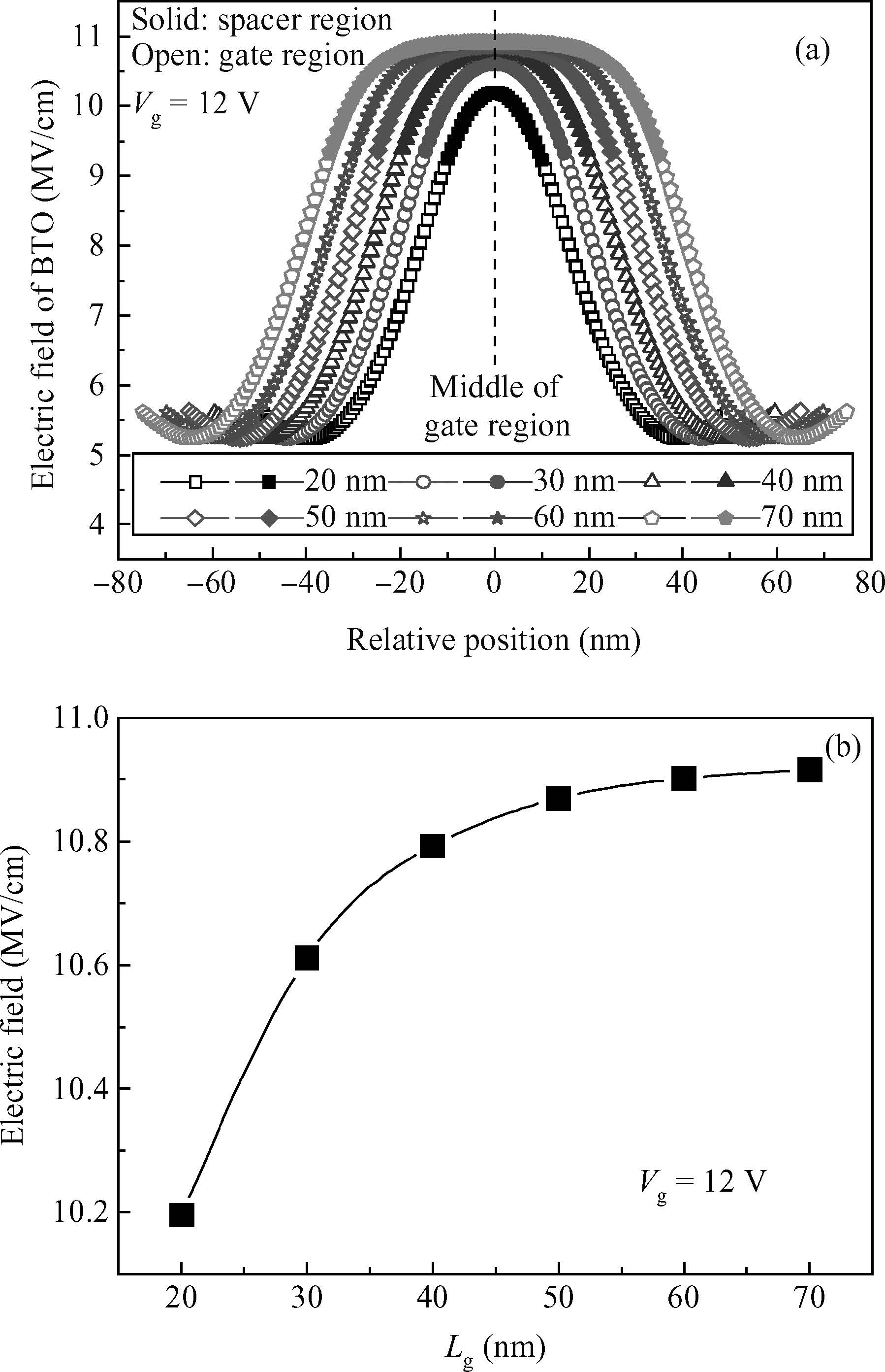
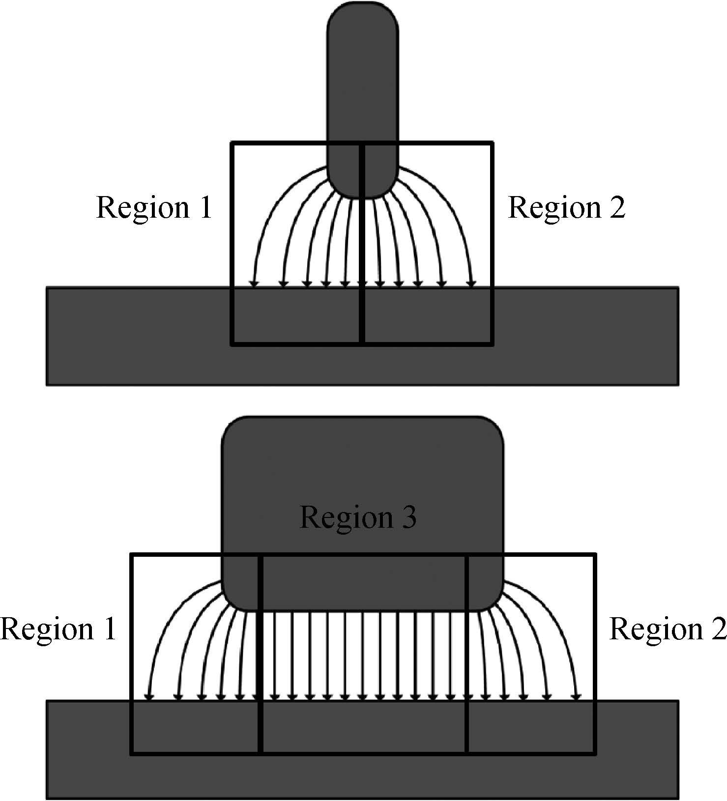
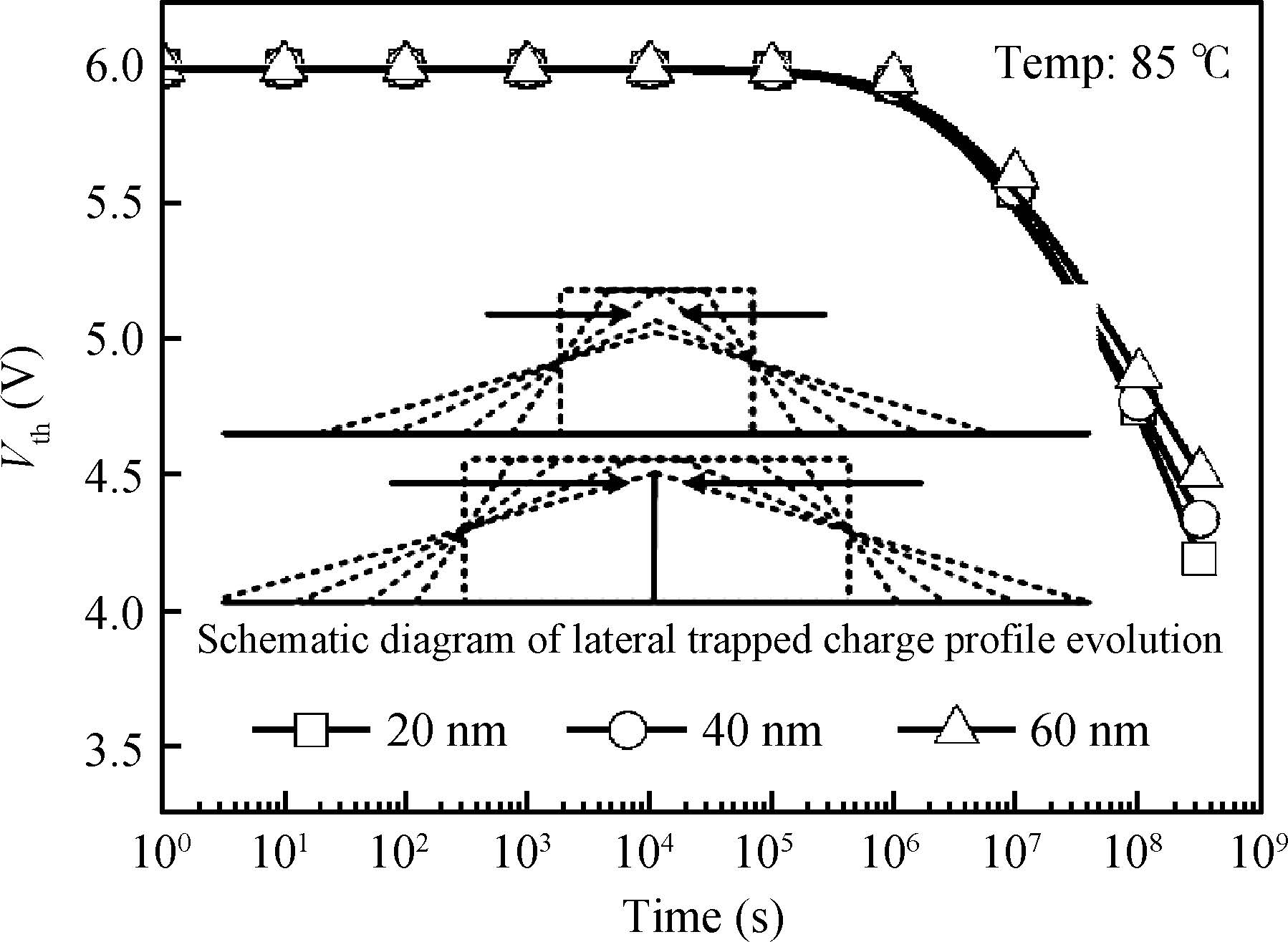
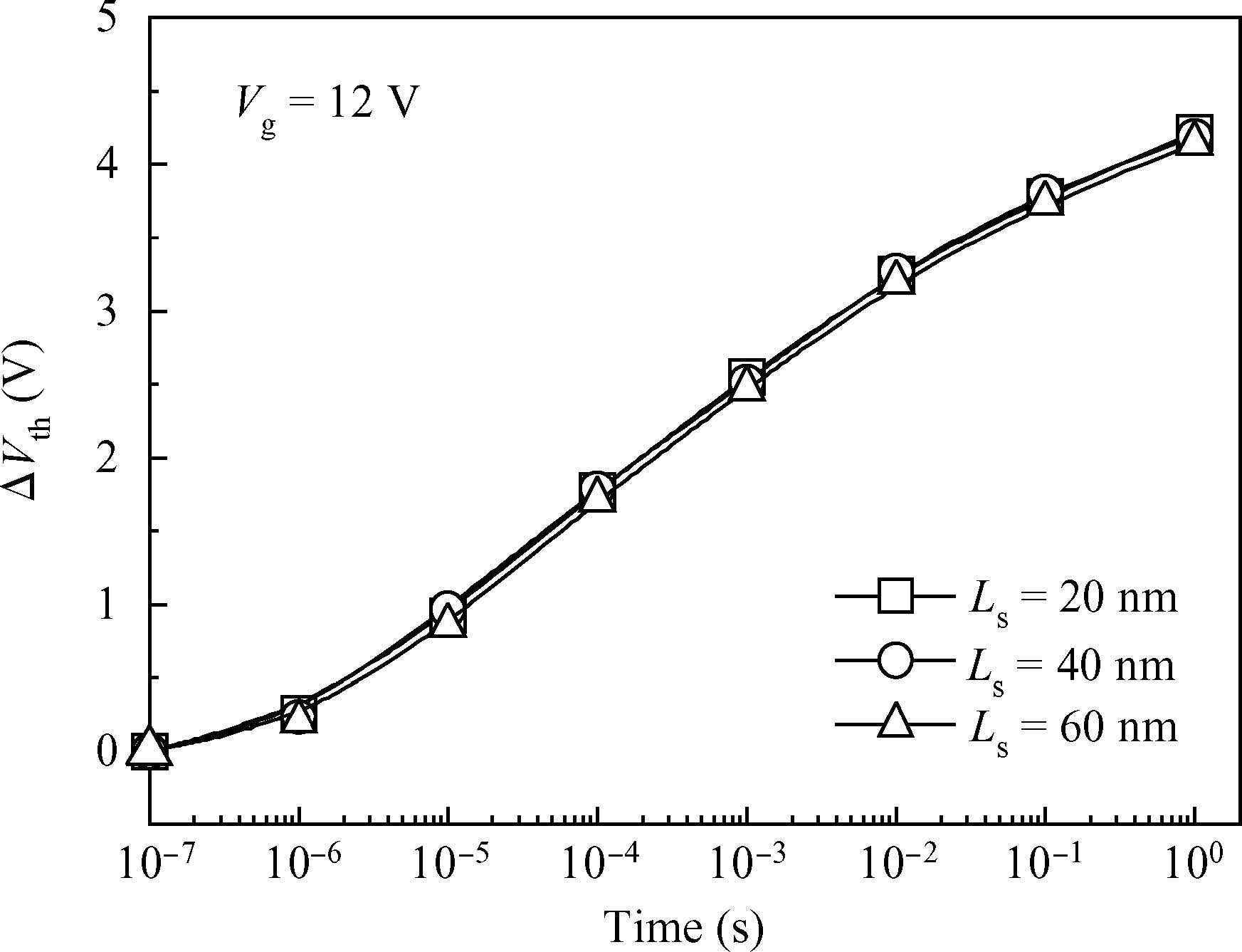
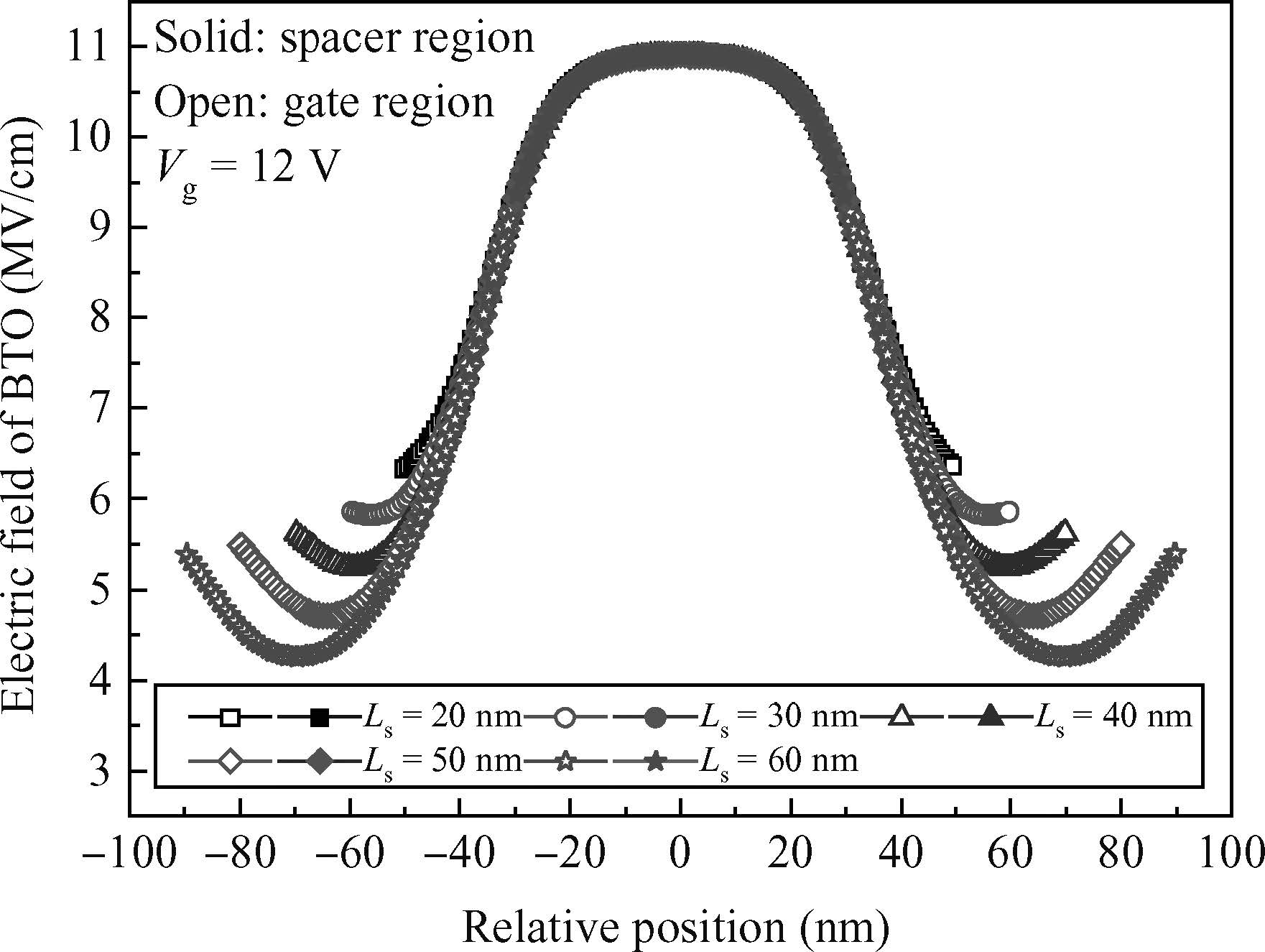
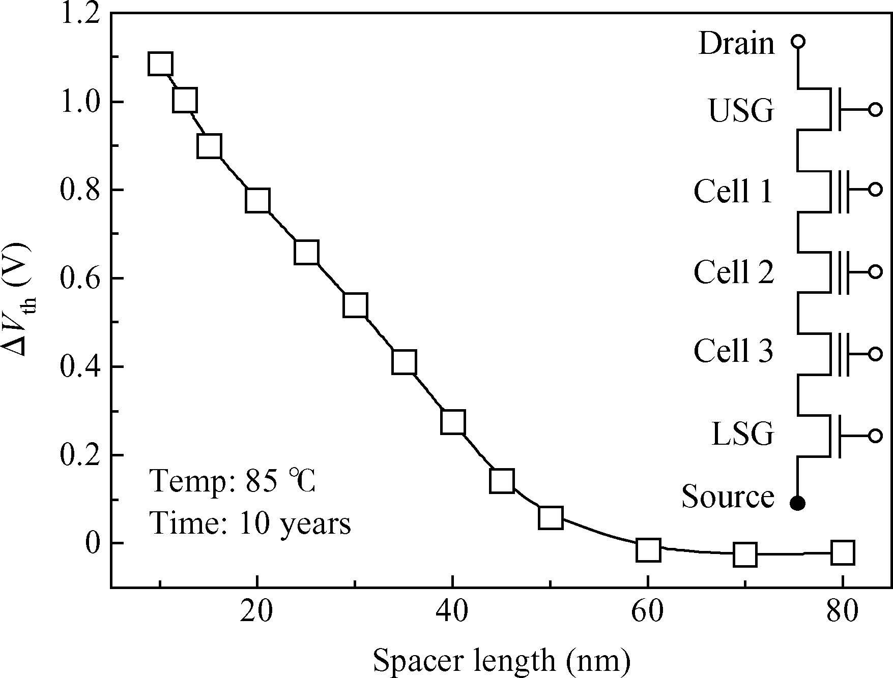
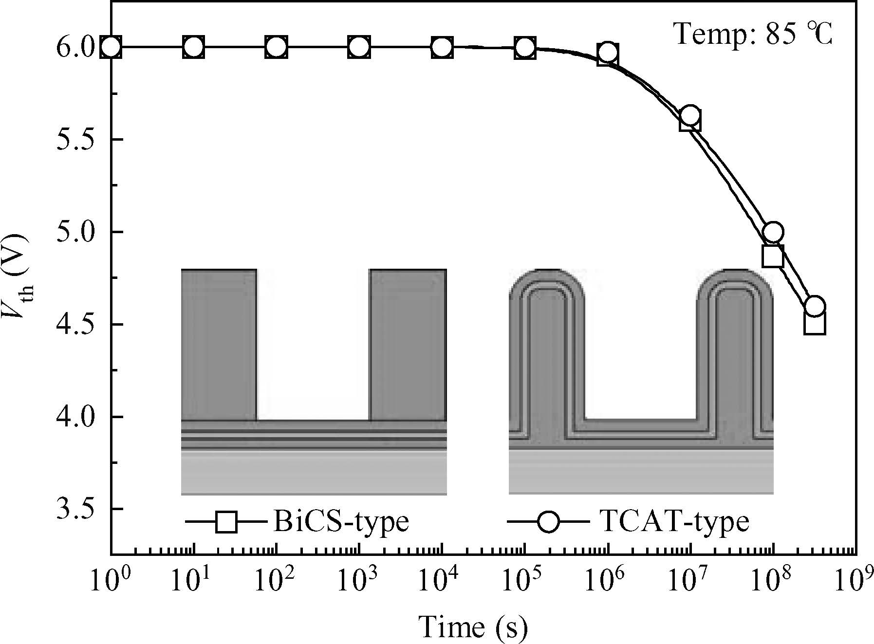
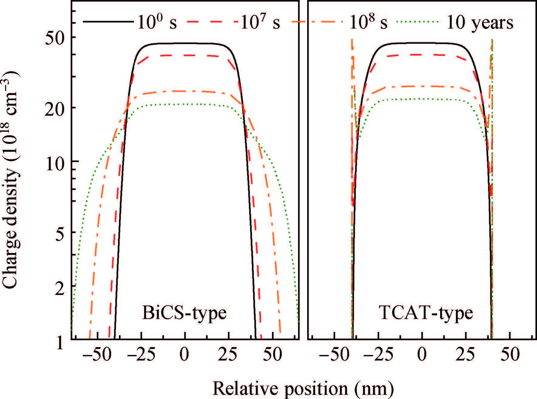
This work presents a comprehensive analysis of 3D cylindrical junction-less charge trapping memory device performance regarding continuous scaling of the structure dimensions. The key device performance, such as program/erase speed, vertical charge loss, and lateral charge migration under high temperature are intensively studied using the Sentaurus 3D device simulator. Although scaling of channel radius is beneficial for operation speed improvement, it leads to a retention challenge due to vertical leakage, especially enhanced charge loss through TPO. Scaling of gate length not only decreases the program/erase speed but also leads to worse lateral charge migration. Scaling of spacer length is critical for the interference of adjacent cells and should be carefully optimized according to specific cell operation conditions. The gate stack shape is also found to be an important factor affecting the lateral charge migration. Our results provide guidance for high density and high reliability 3D CTM integration.
J. Semicond.
2015, 36(9): 094009 doi: 10.1088/1674-4926/36/9/094009

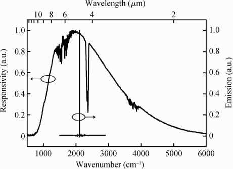
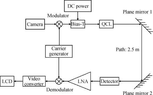
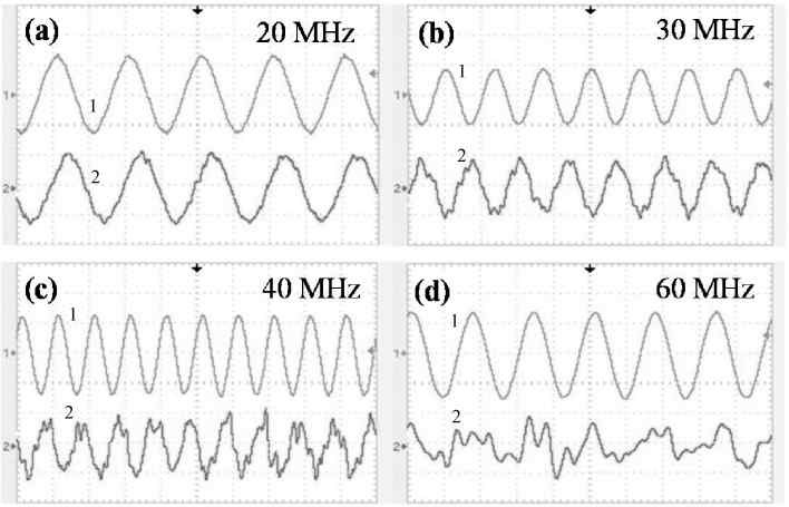
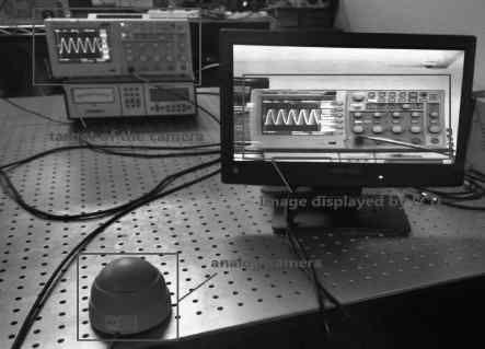
A free-space communication based on a mid-infrared quantum cascade laser (QCL) is presented. A room-temperature continuous-wave distributed-feedback (DFB) QCL combined with a mid-infrared detector comprise the basic unit of the communication system. Sinusoidal signals at a highest frequency of 40 MHz and modulated video signals with a carrier frequency of 30 MHz were successfully transmitted with this experimental setup. Our research has provided a proof-of-concept demonstration of space optical communication application with QCL. The highest operation frequency of our setup was determined by the circuit-limited modulation bandwidth. A high performance communication system can be obtained with improved modulation circuit system.
J. Semicond.
2015, 36(9): 094010 doi: 10.1088/1674-4926/36/9/094010

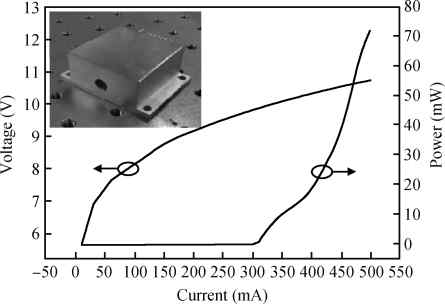
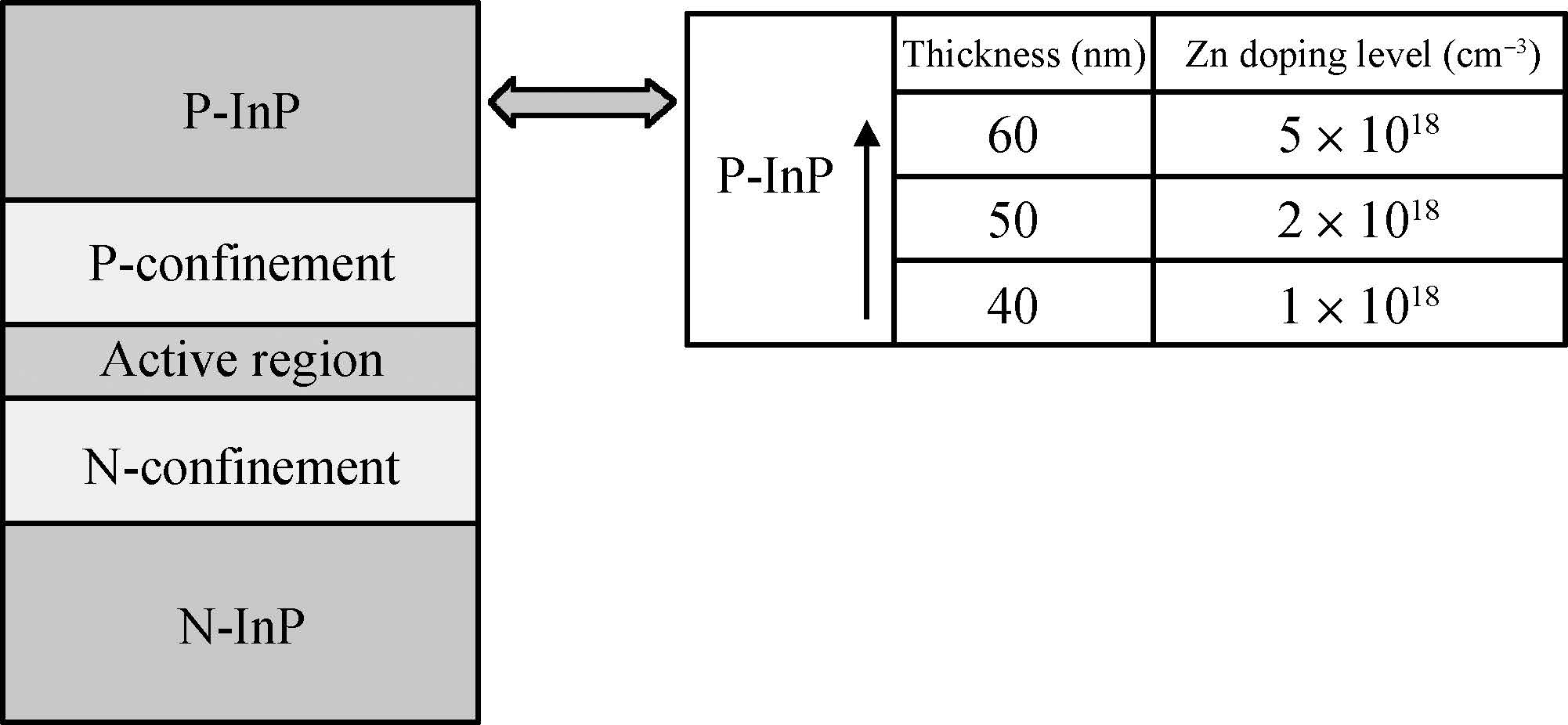
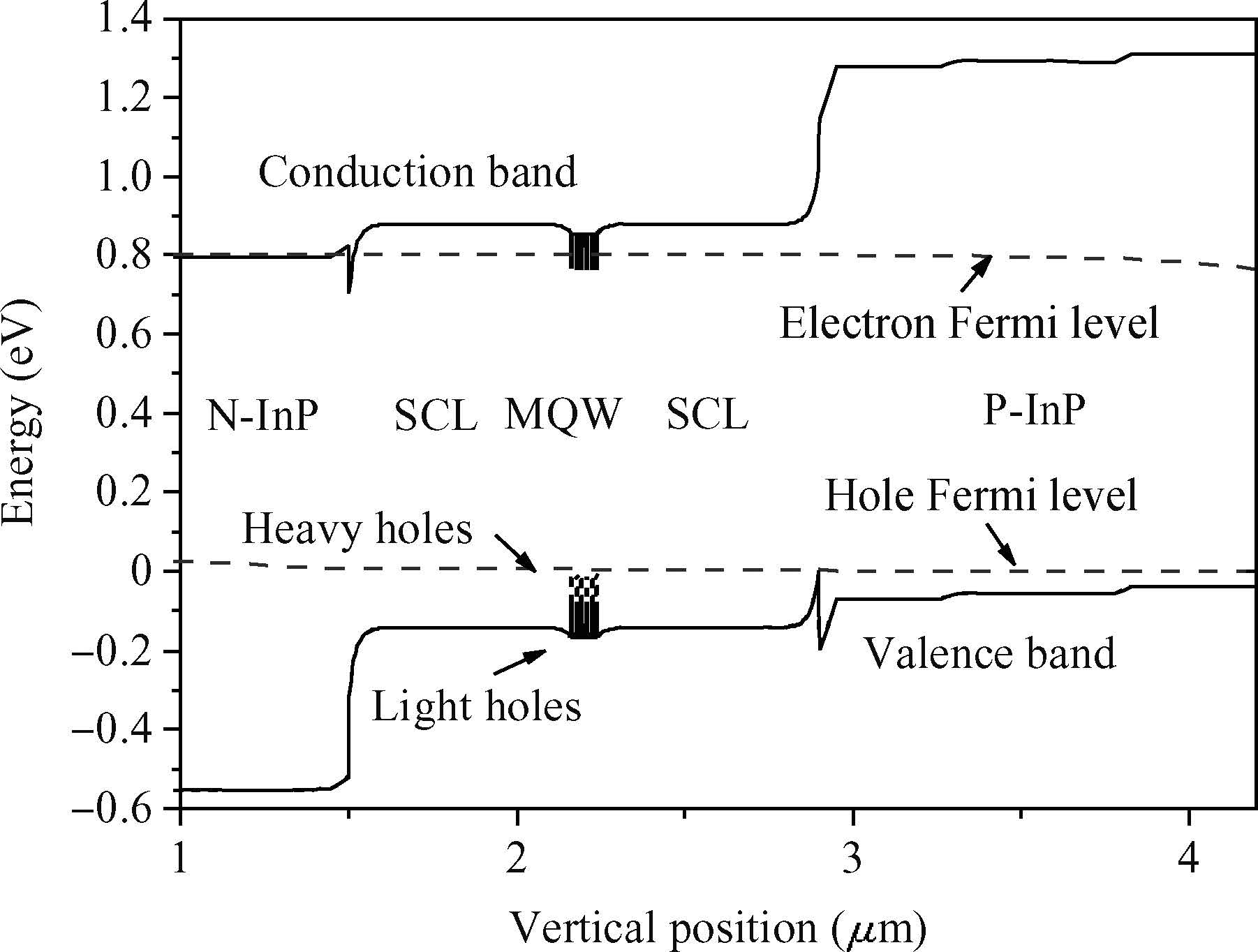
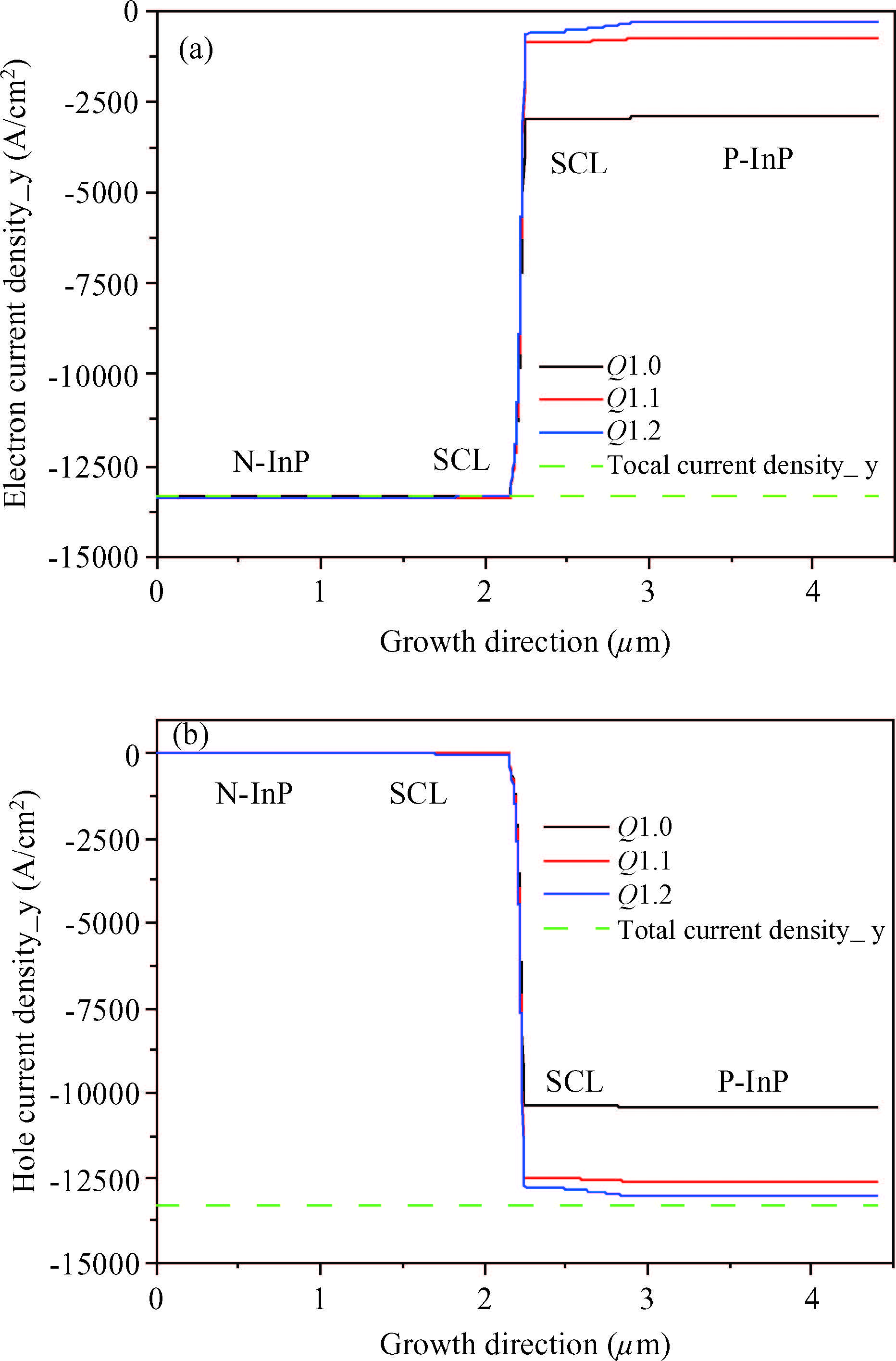
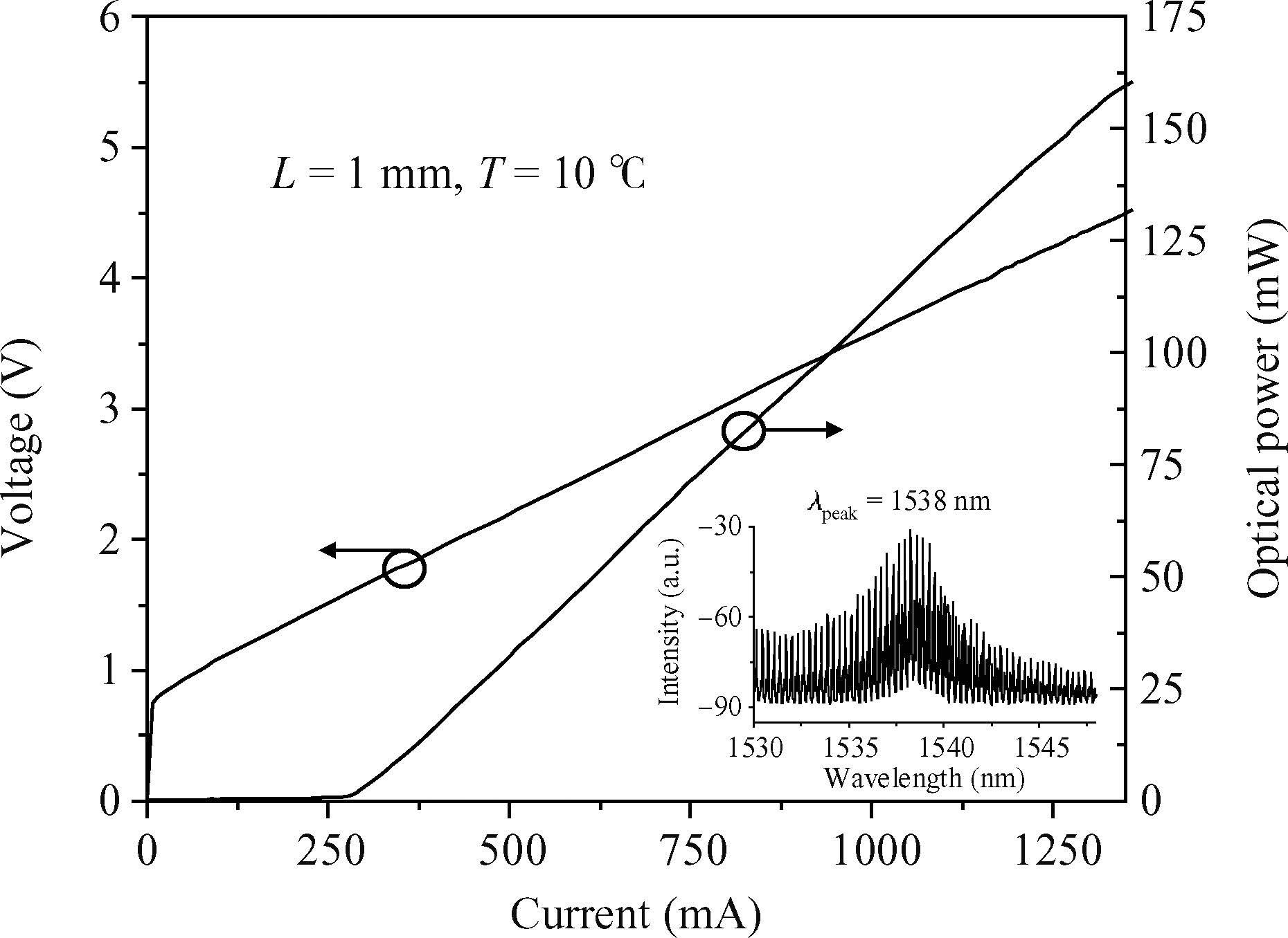
A comprehensive design optimization of 1.55-μm high power InGaAsP/InP board area lasers is performed aiming at increasing the internal quantum efficiency (ηi) while maintaining the low internal loss (αi) of the device, thereby achieving high power operation. Four different waveguide structures of broad area lasers were fabricated and characterized in depth. Through theoretical analysis and experiment verifications, we show that laser structures with stepped waveguide and thin upper separate confinement layer will result in high ηi and overall slope efficiency. A continuous wave (CW) single side output power of 160 mW was obtained for an uncoated laser with a 50-μm active area width and 1 mm cavity length.
J. Semicond.
2015, 36(9): 094011 doi: 10.1088/1674-4926/36/9/094011

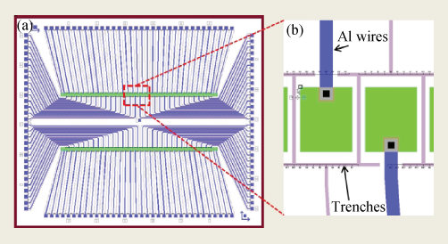
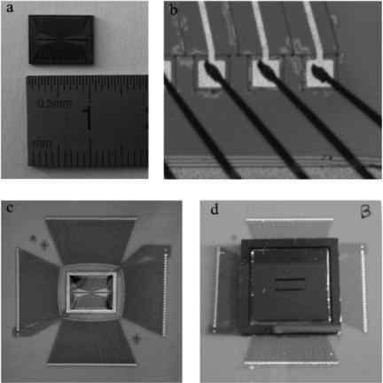
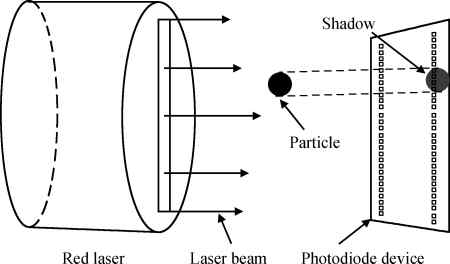
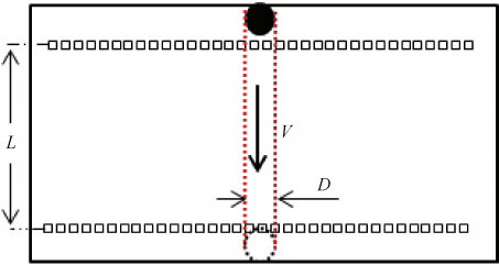
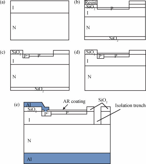
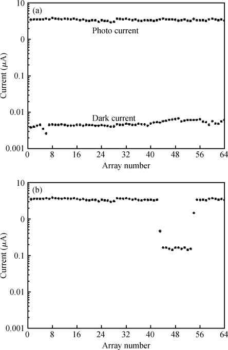
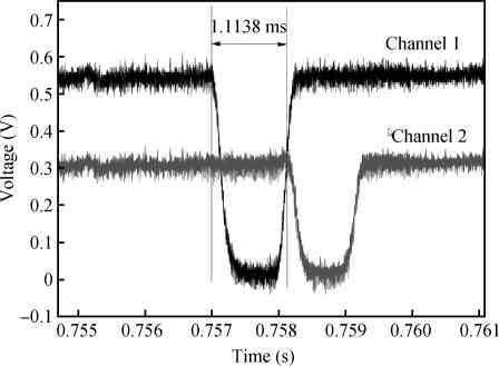
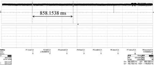
A novel PIN (positive-intrinsic-negative) photodetector with double linear arrays that can be used to measure the diameter of precipitation particles and the space between two droplets in clouds is proposed. The sensitive unit is the PIN photodiode. The chip with a size of 10 × 8 mm2 has 128 photodiodes, and each row has 64 photodiodes. The device design, fabrication process and package are introduced in the paper. The photocurrent of the packaged chip was systematically tested with a red laser. Also the diameter of one water drop and the space between two water drops were measured. The minimum raindrop diameter which can be tested in this paper is 100μm. This device can be useful for rainfall prediction.
J. Semicond.
2015, 36(9): 094012 doi: 10.1088/1674-4926/36/9/094012

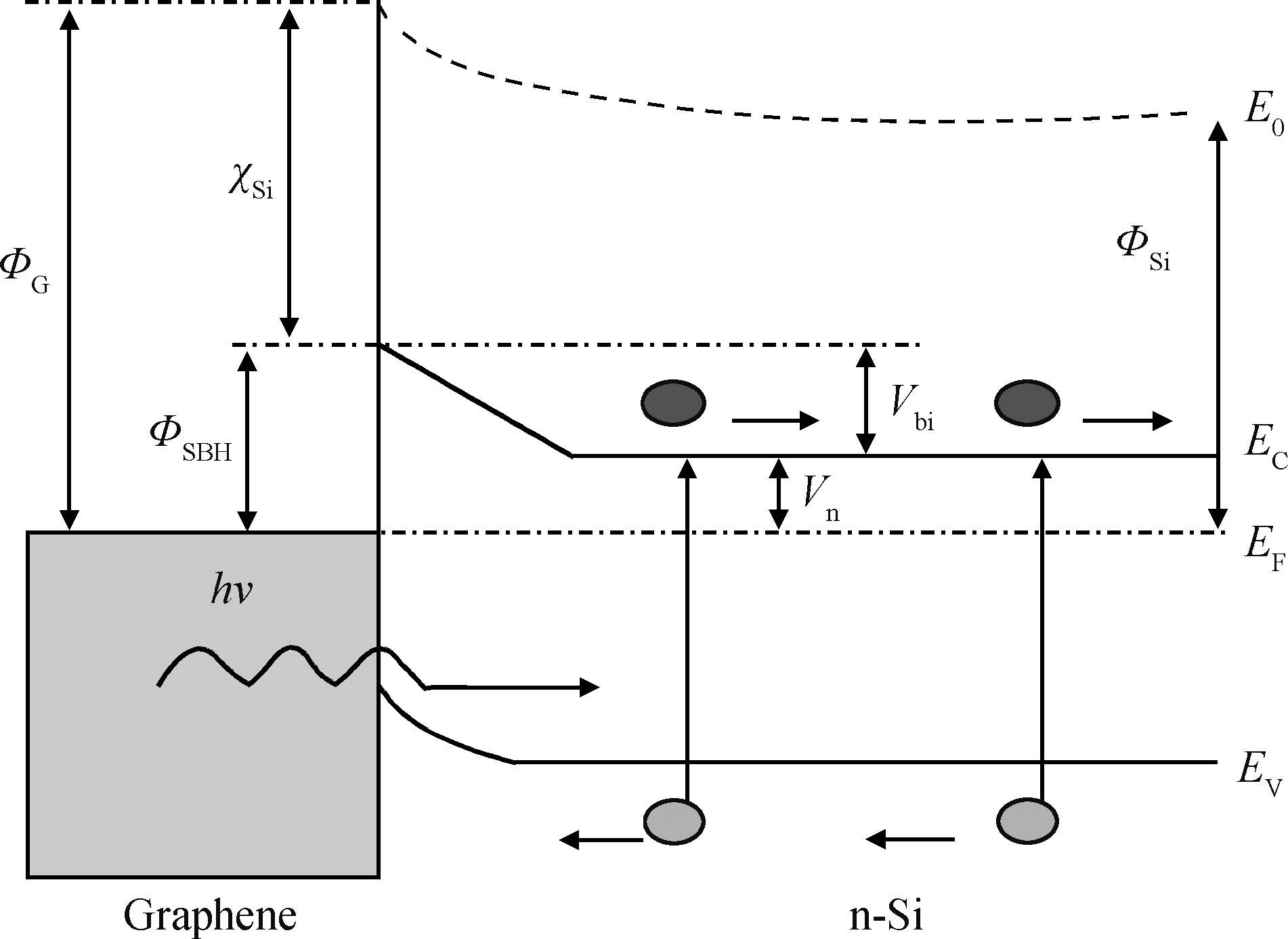
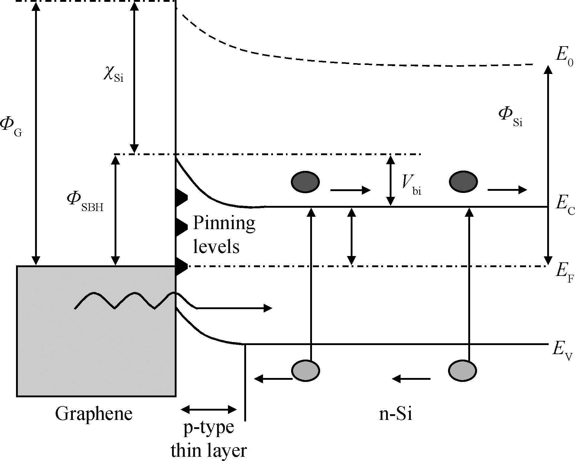
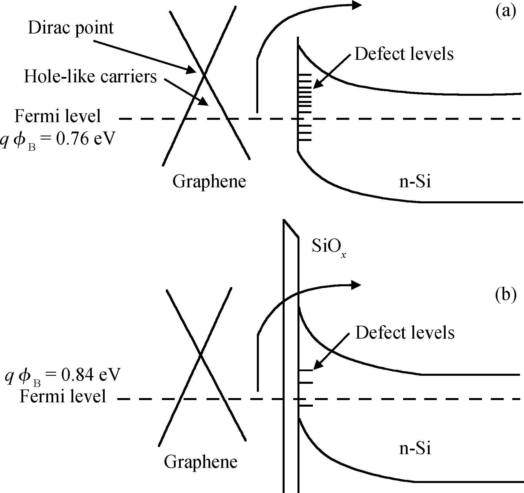
In a recent article, Chen et al. [Electrochimica Acta, 2014, 130: 279] presented their fabrication and characterization results on a graphene/n-Si solar cell where the Au nanoparticles were inserted in graphene to increase its optical and electrical properties. The higher efficiency of the device was attributed to increased conductivity of graphene after doping with Au nanoparticles. However, the knowledge in the field of Schottky diode solar cells relates this to increased band bending at the junction. Also, to explain the instability behaviour, they concluded that the growth of silicon oxide on the Si surface or oxygen adsorption on the window layer resulted in the device performance increasing initially and decreasing in the end. However, this instability seems to be due to variation in series resistance reduced at the beginning because of slightly lowered Fermi level and increased at the end by the self-compensation by deep in-diffusion of Au nanoparticles into n-Si layer. We also propose that inserting a very thin p-type layer at the junction will enhance the carrier collection and performance of this device.
J. Semicond.
2015, 36(9): 095001 doi: 10.1088/1674-4926/36/9/095001

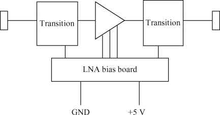
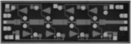
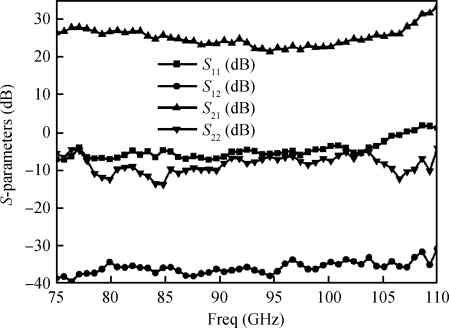
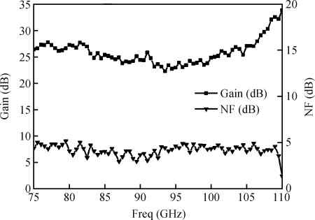
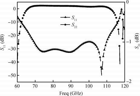
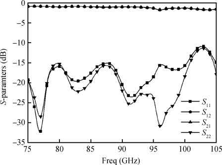
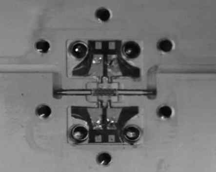
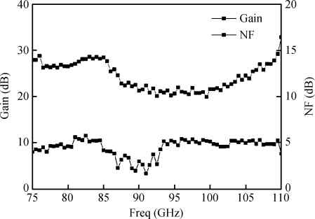
A full W-band low noise amplifier (LNA) module is designed and fabricated. A broadband transition is introduced in this module. The proposed transition is designed,optimized based on the results from numerical simulations. The results show that 1 dB bandwidth of the transition ranges from 61 to 117 GHz. For the purpose of verification,two transitions in back-to-back connection are measured. The results show that transmission loss is only about 0.9-1.7 dB. This transition is used to interface integrated circuits to waveguide components. The characteristic of the LNA module is measured after assembly. It exhibits a broad bandwidth of 75 to 110 GHz,and has a small signal gain above 21 dB. The noise figure is lower than 5.2 dB throughout the entire W-band (below 3 dB from 89 to 95 GHz) at room temperature. The proposed LNA module exhibits potential for millimeter wave applications due to its high small signal gain,low noise,and low DC power consumption.

J. Semicond.
2015, 36(9): 095002 doi: 10.1088/1674-4926/36/9/095002

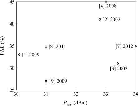
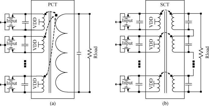
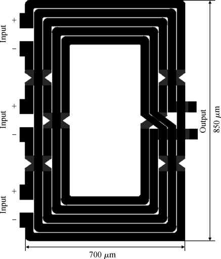
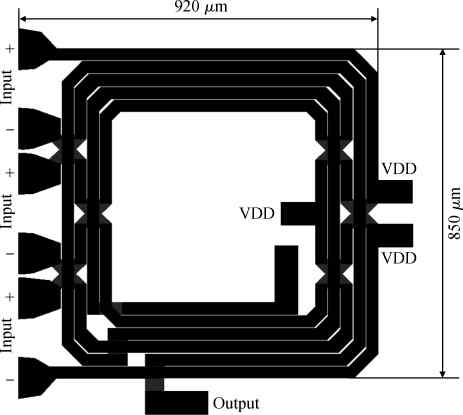
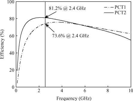
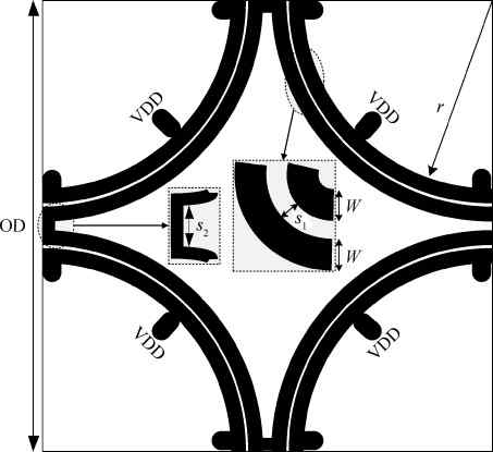
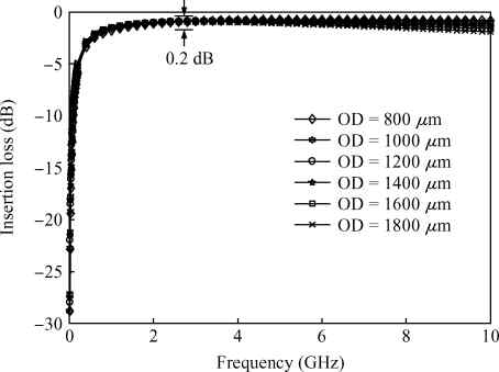
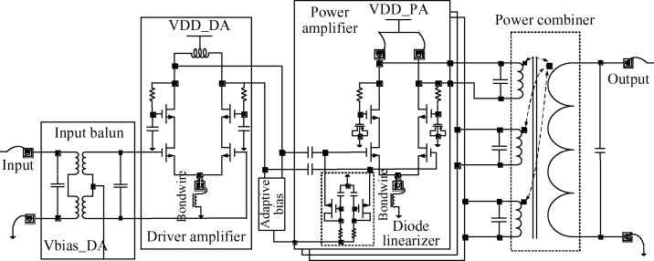
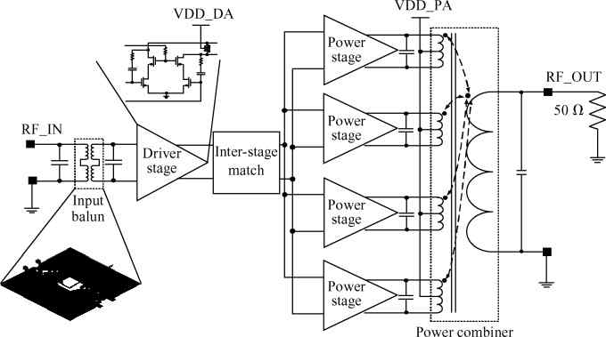
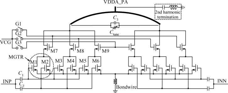
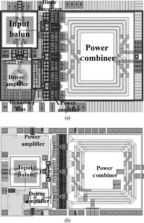
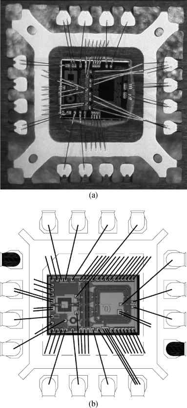
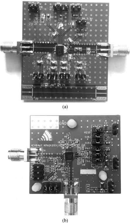
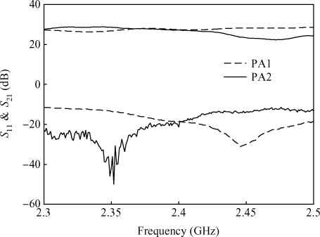
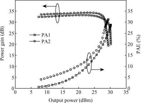
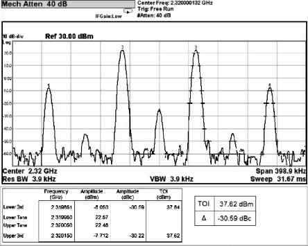
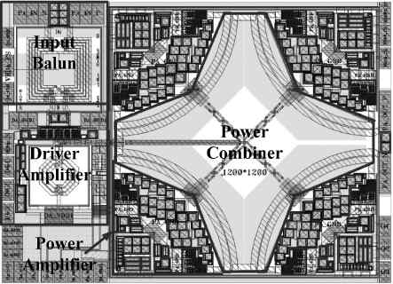
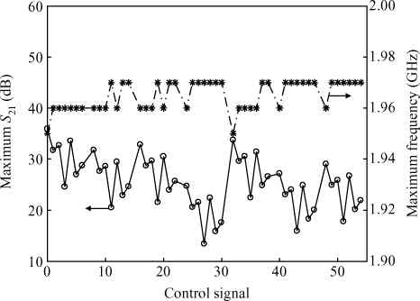
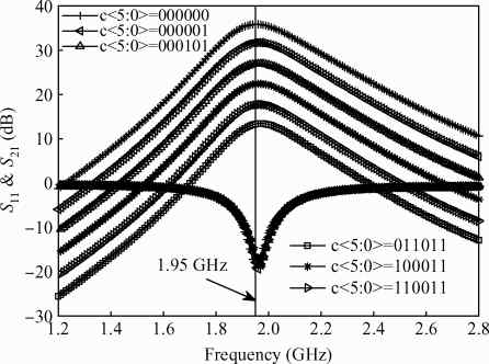
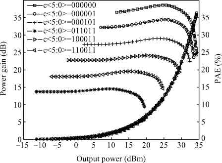
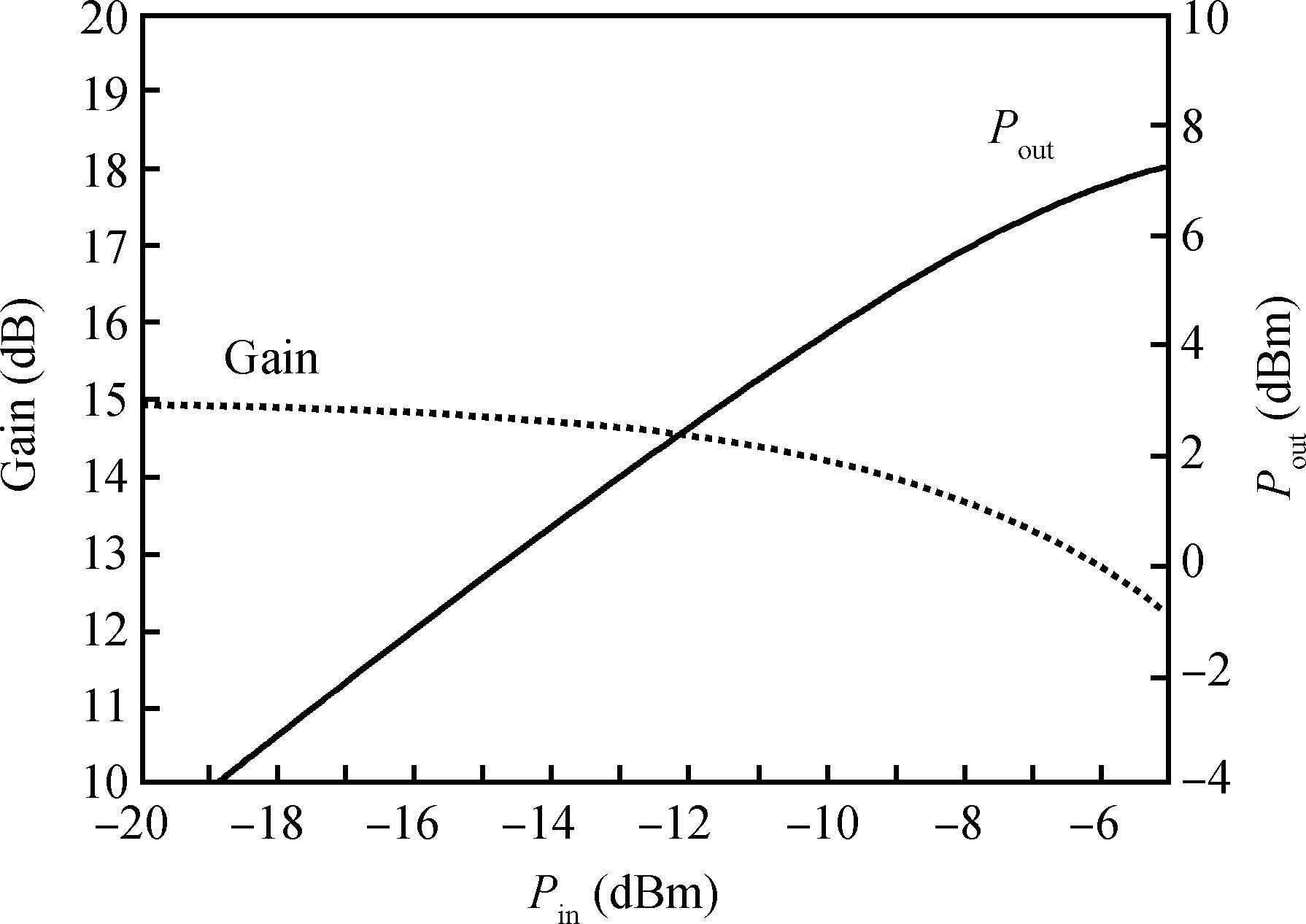
Three linear CMOS power amplifiers (PAs) with high output power (more than watt-level output power) for high data-rate mobile applications are introduced. To realize watt-level output power, there are two 2.4 GHz PAs using an on-chip parallel combining transformer (PCT) and one 1.95 GHz PA using an on-chip series combining transformer (SCT) to combine output signals of multiple power stages. Furthermore, some linearization techniques including adaptive bias, diode linearizer, multi-gated transistors (MGTR) and the second harmonic control are applied in these PAs. Using the proposed power combiner, these three PAs are designed and fabricated in TSMC 0.18 μm RFCMOS process. According to the measurement results, the proposed two linear 2.4 GHz PAs achieve a gain of 33.2 dB and 34.3 dB, a maximum output power of 30.7 dBm and 29.4 dBm, with 29% and 31.3% of peak PAE, respectively. According to the simulation results, the presented linear 1.95 GHz PA achieves a gain of 37.5 dB, a maximum output power of 34.3 dBm with 36.3% of peak PAE.
J. Semicond.
2015, 36(9): 095003 doi: 10.1088/1674-4926/36/9/095003

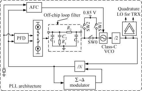
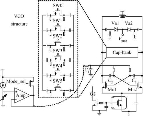
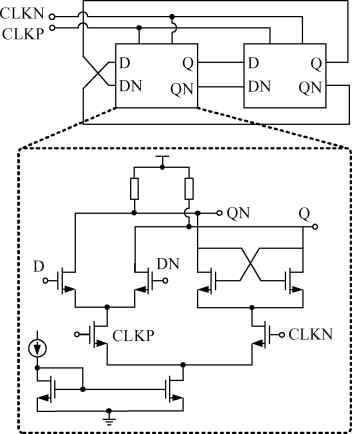
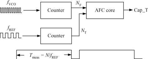
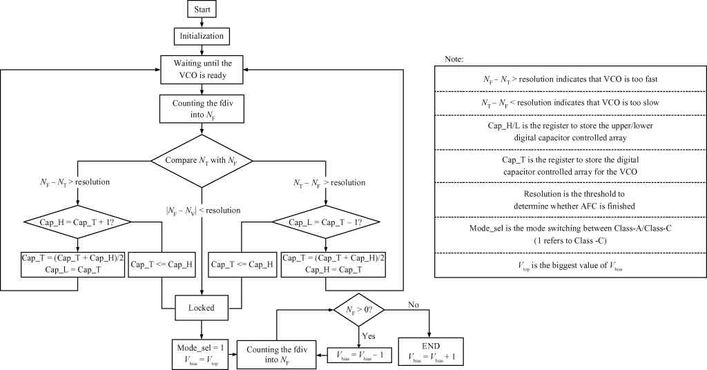
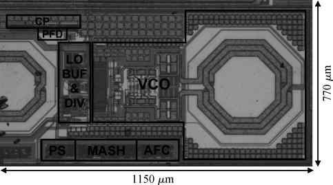
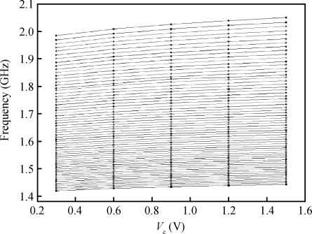
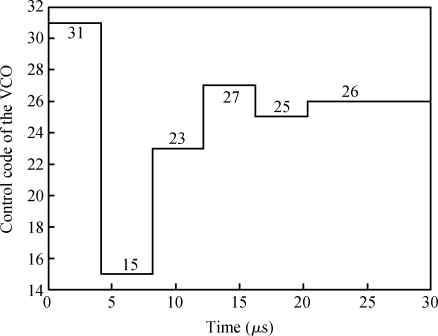
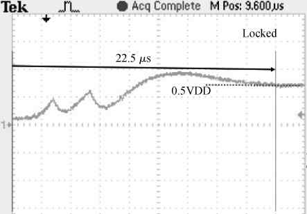
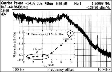
A 1.4-2 GHz phase-locked loop (PLL) Σ-Δ fraction-N frequency synthesizer with automatic frequency control (AFC) for 802.11ah applications is presented. A class-C voltage control oscillator (VCO) ranging from 1.4 to 2 GHz is integrated on-chip to save power for the sub-GHz band. A novel AFC algorithm is introduced to maintain the VCO oscillation at the start-up and automatically search for the appropriate control word of the switched-capacitor array to extend the PLL tuning range. A 20-bit third-order Σ-Δ modulator is utilized to reduce the fraction spurs while achieving a frequency resolution that is lower than 30 Hz. The measurement results show that the frequency synthesizer has achieved a phase noise of < -120 dBc/Hz at 1 MHz offset and consumes 11.1 mW from a 1.7 V supply. Moreover,compared with the traditional class-A counterparts,the phase noise in class-C mode has been improved by 5 dB under the same power consumption.
J. Semicond.
2015, 36(9): 095004 doi: 10.1088/1674-4926/36/9/095004

According to the specific input-output characteristics of a pressure sensor, a novel calibration algorithm is presented and a calibration system is developed to correct the nonlinear error caused by temperature. In contrast to the routine BP and RBF, curve fitting based on RBF is first used to get the slope and intercept, and then the voltage-pressure curve is described. Test results show that the algorithm features fast convergence speed, strong robustness and minimum SSE (sum of squares for error). It is proven by practical applications that this calibration system works well and the measurement precision is better than the design demands. Furthermore, this calibration system has a good real-time capability.


J. Semicond.
2015, 36(9): 095005 doi: 10.1088/1674-4926/36/9/095005

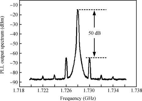
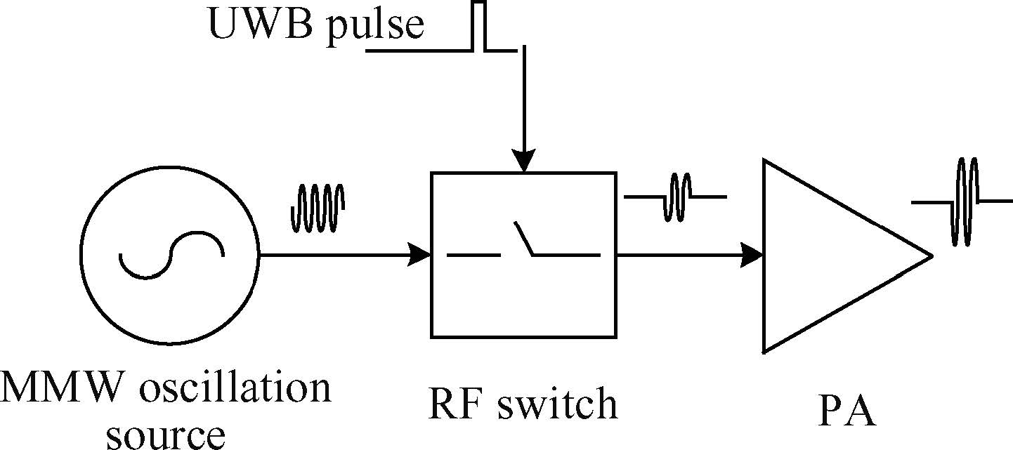
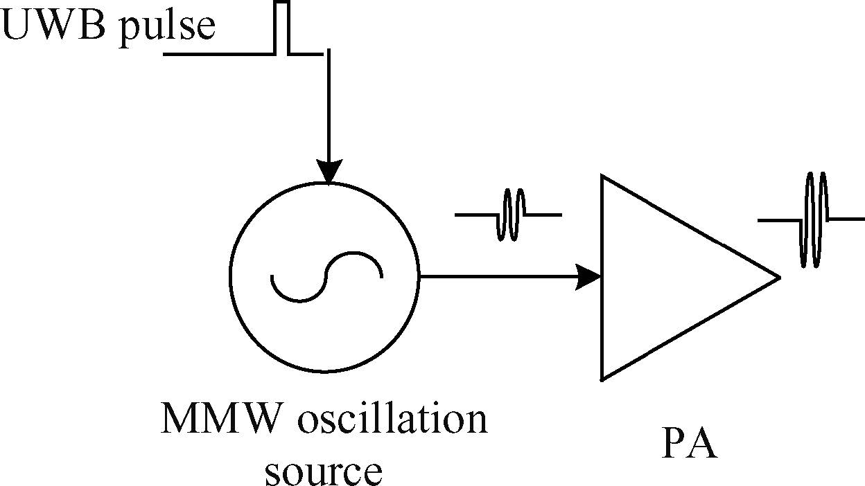
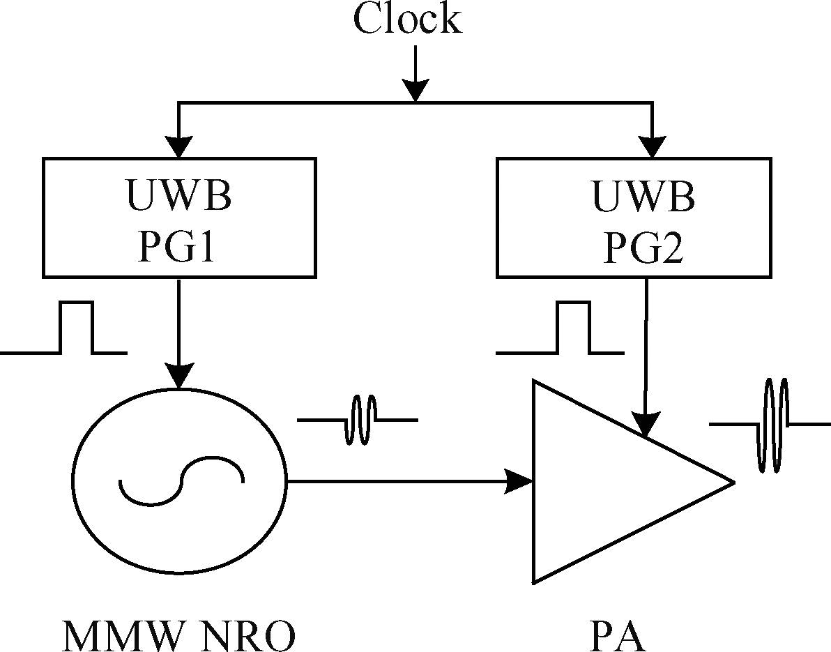
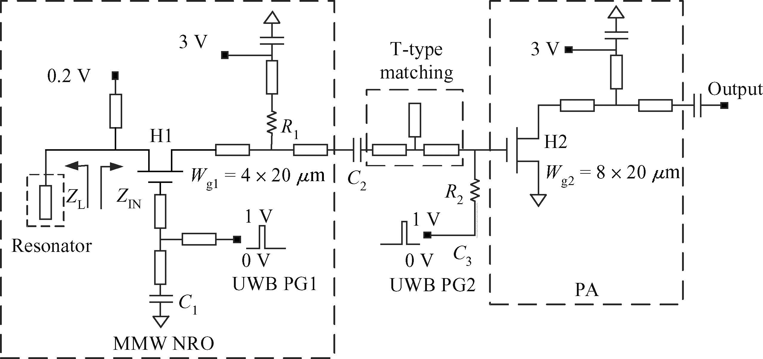
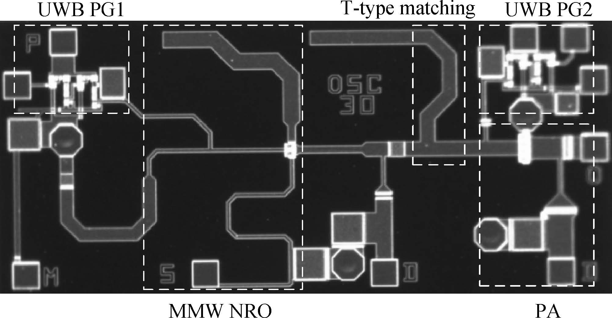
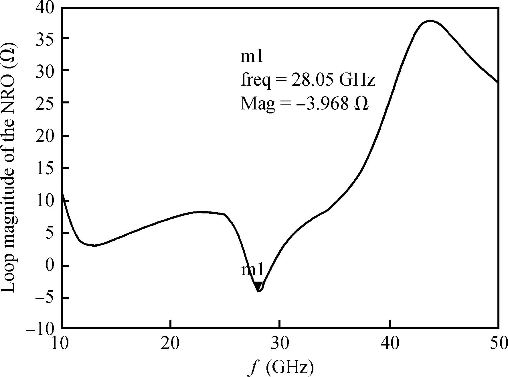
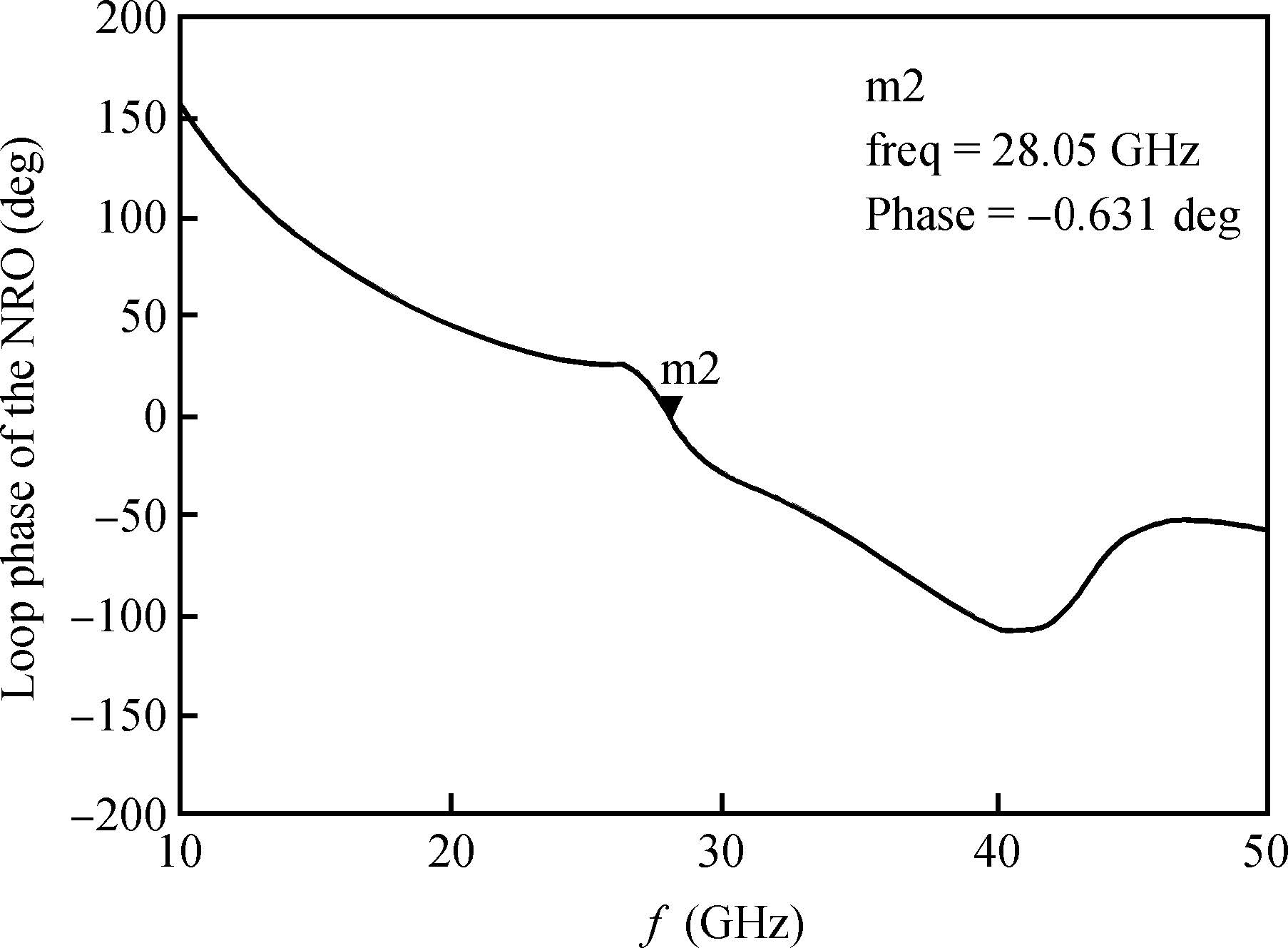
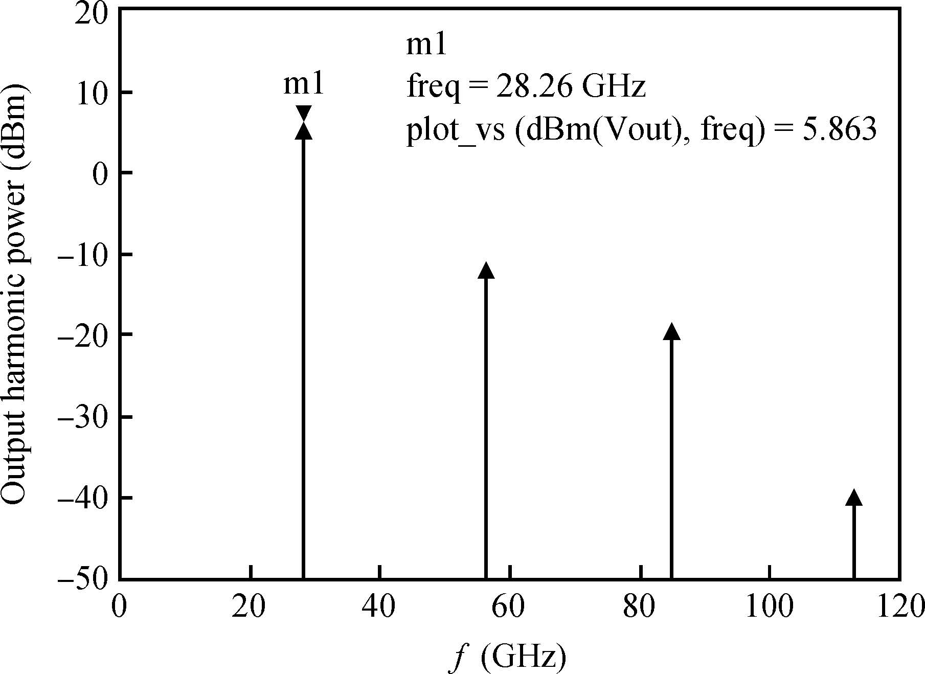
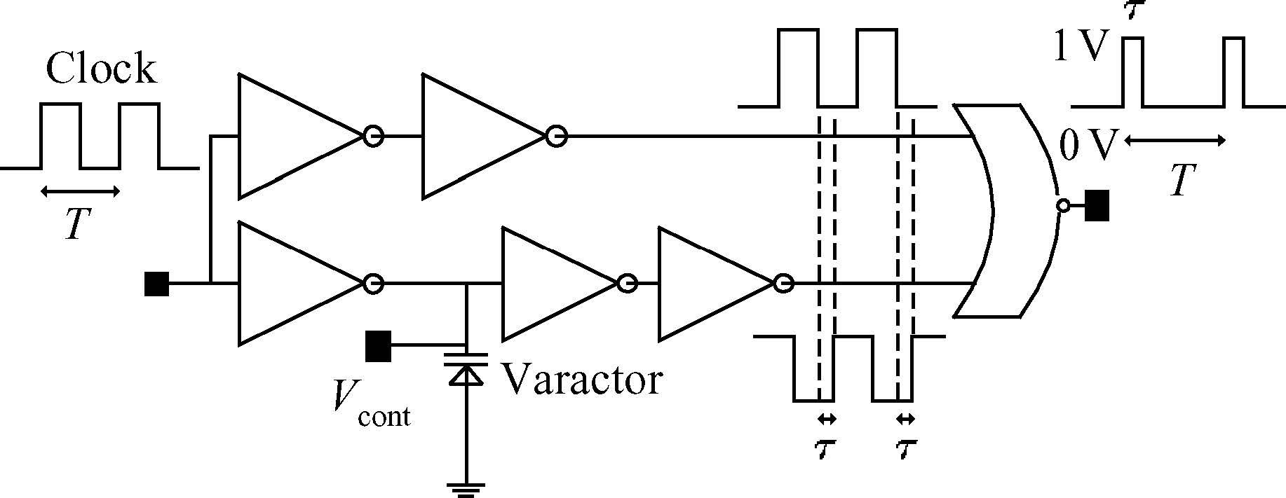
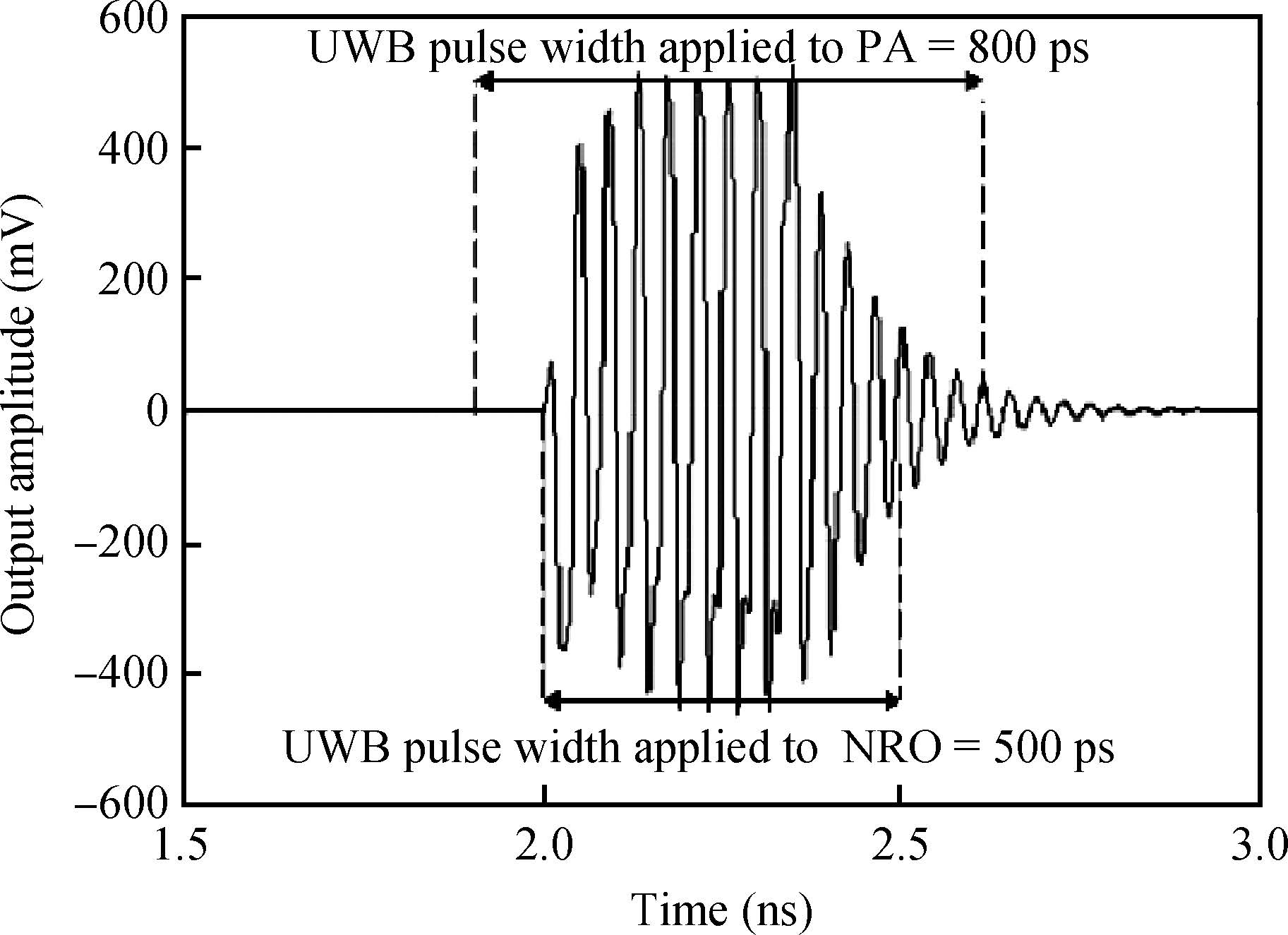
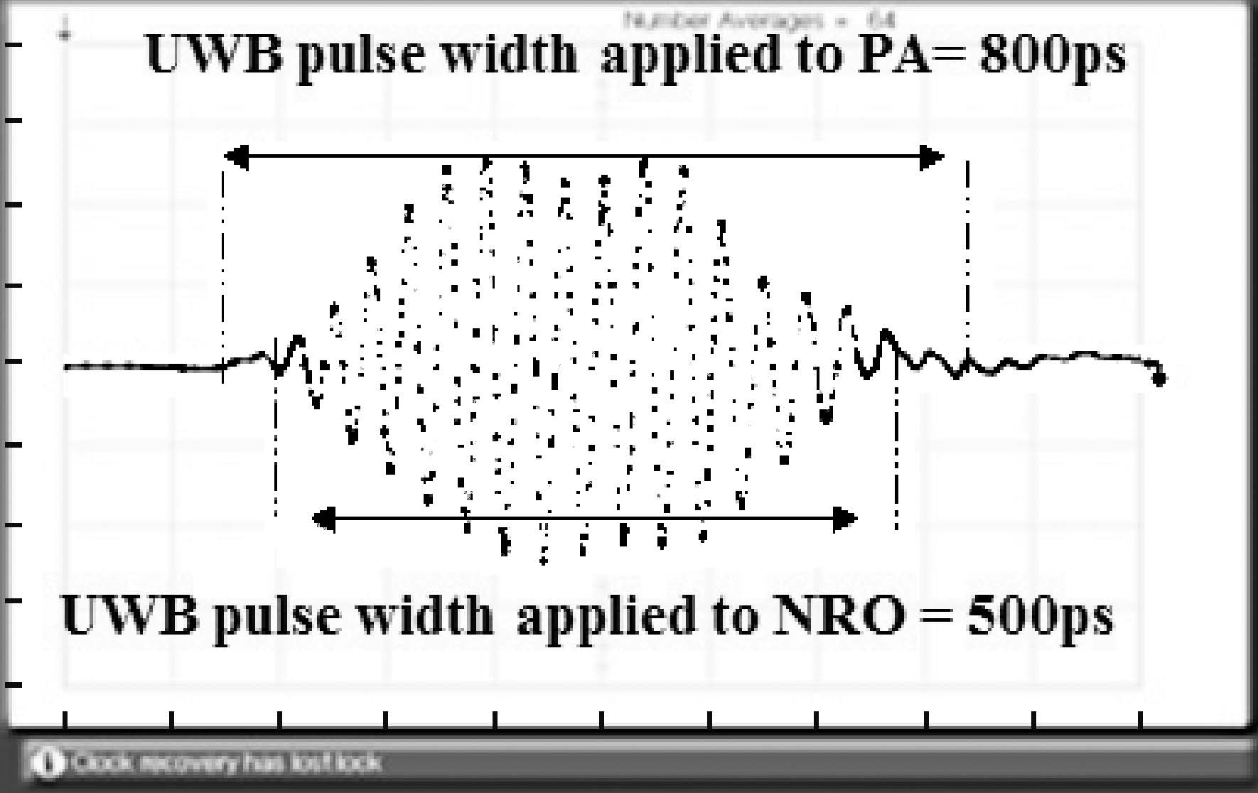
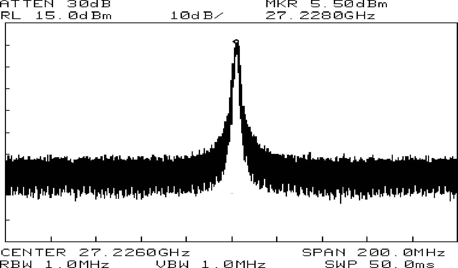
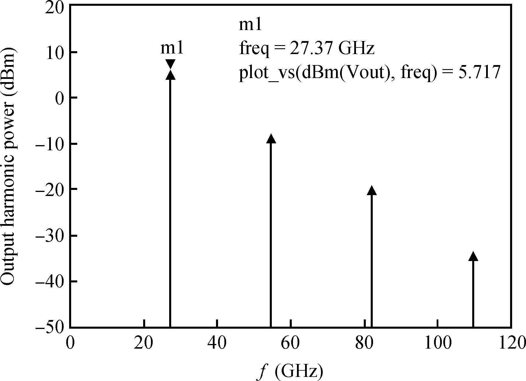
This paper presents a new millimeter-wave (MMW) ultra wideband (UWB) transmitter MMIC which has been developed in an OMMIC 0.1 μm GaAs PHEMT foundry process (ft = 100 GHz) for 22-29 GHz vehicular radar systems. The transmitter is composed of an MMW negative resistance oscillator (NRO), a power amplifier (PA), and two UWB pulse generators (PGs). In order to convert the UWB pulse signal to MMW frequency and reduce the total power consumption, the MMW NRO is driven by one of the UWB pulse generators and the power amplifier is triggered by another UWB pulse generator. The main advantages of this transmitter are: new design, simple architecture, high-precision distance measurements, infinite ON/OFF switch ratio, and low power consumption. The total power consumption of the transmitter MMIC is 218 mW with a peak output power of 5.5 dBm at 27 GHz.
J. Semicond.
2015, 36(9): 095006 doi: 10.1088/1674-4926/36/9/095006

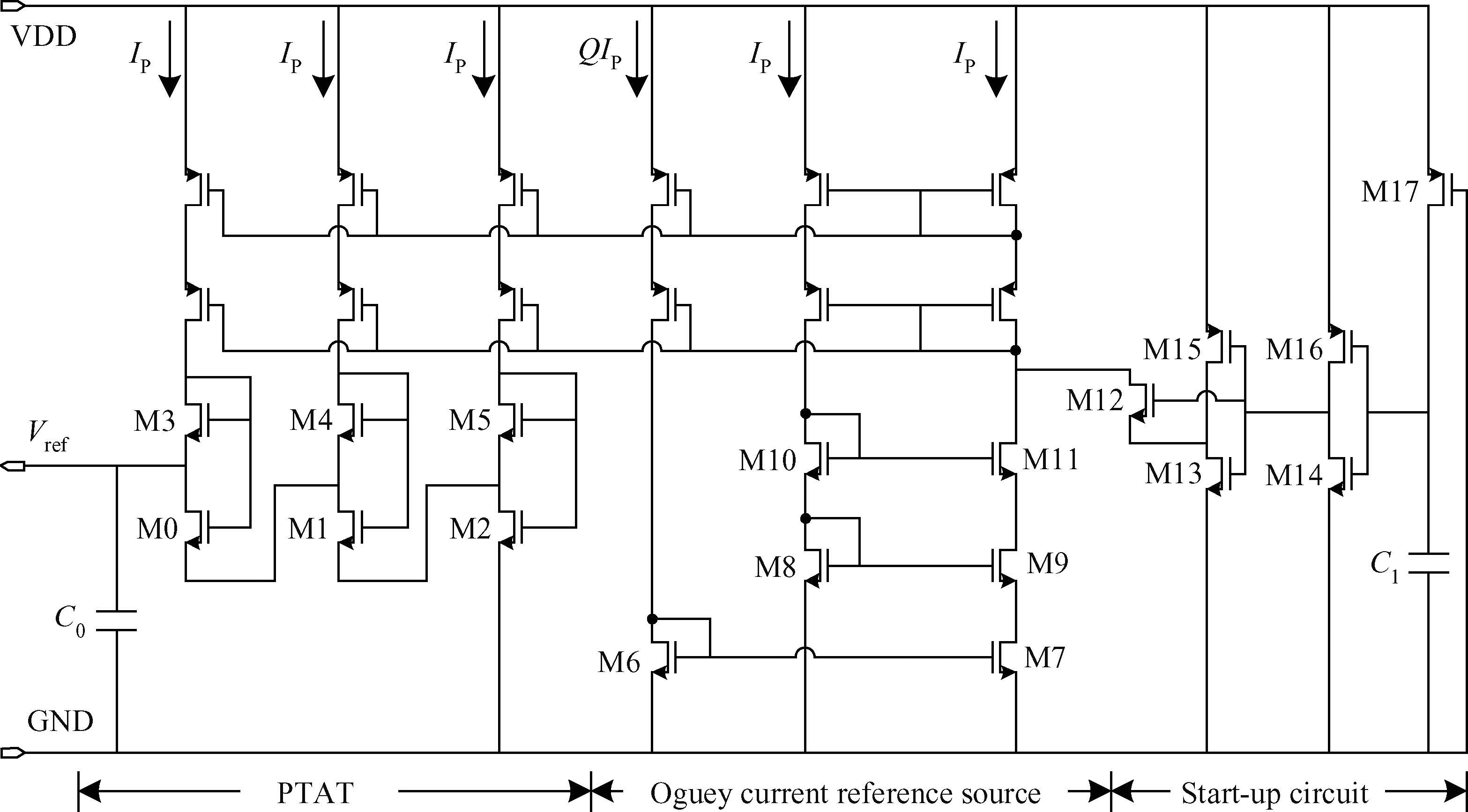
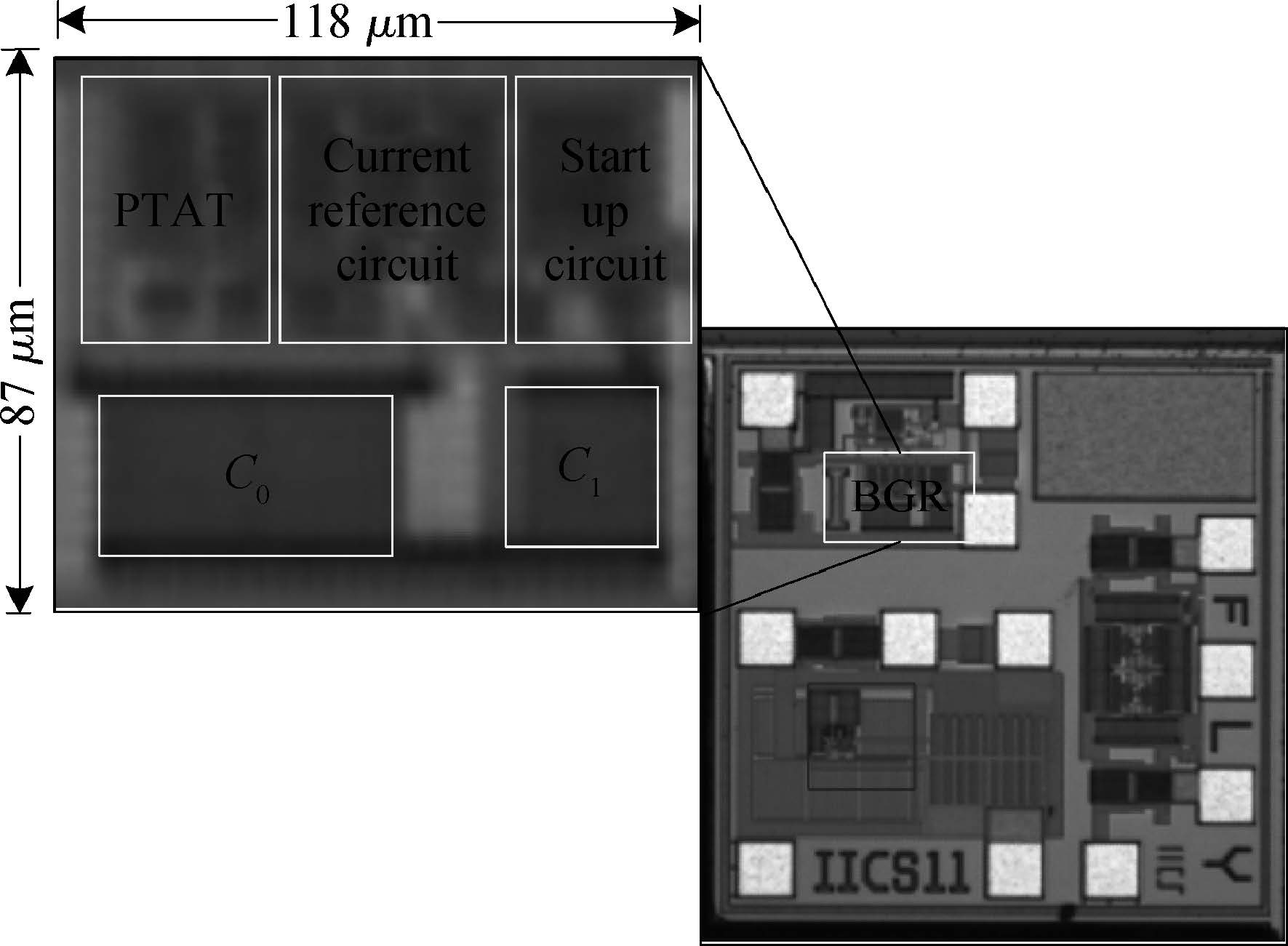
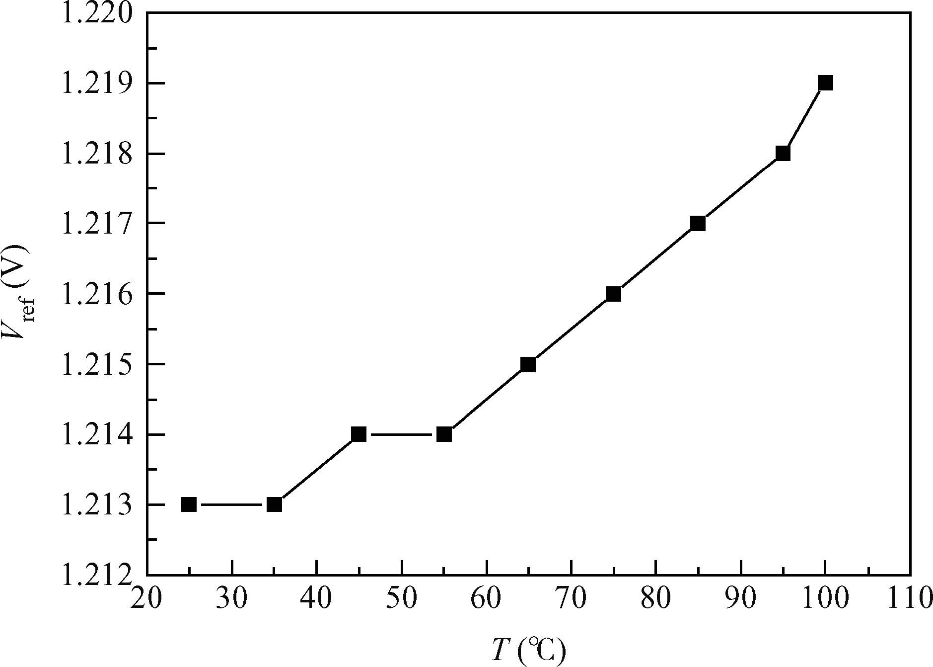
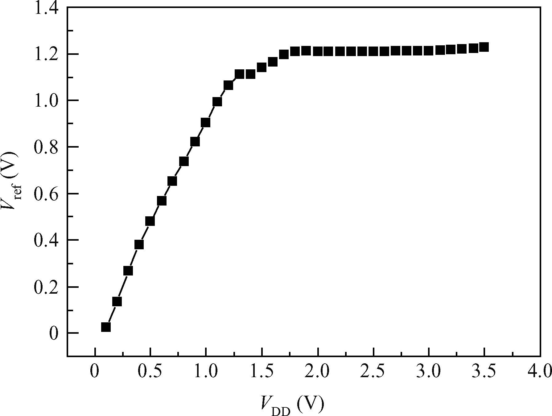
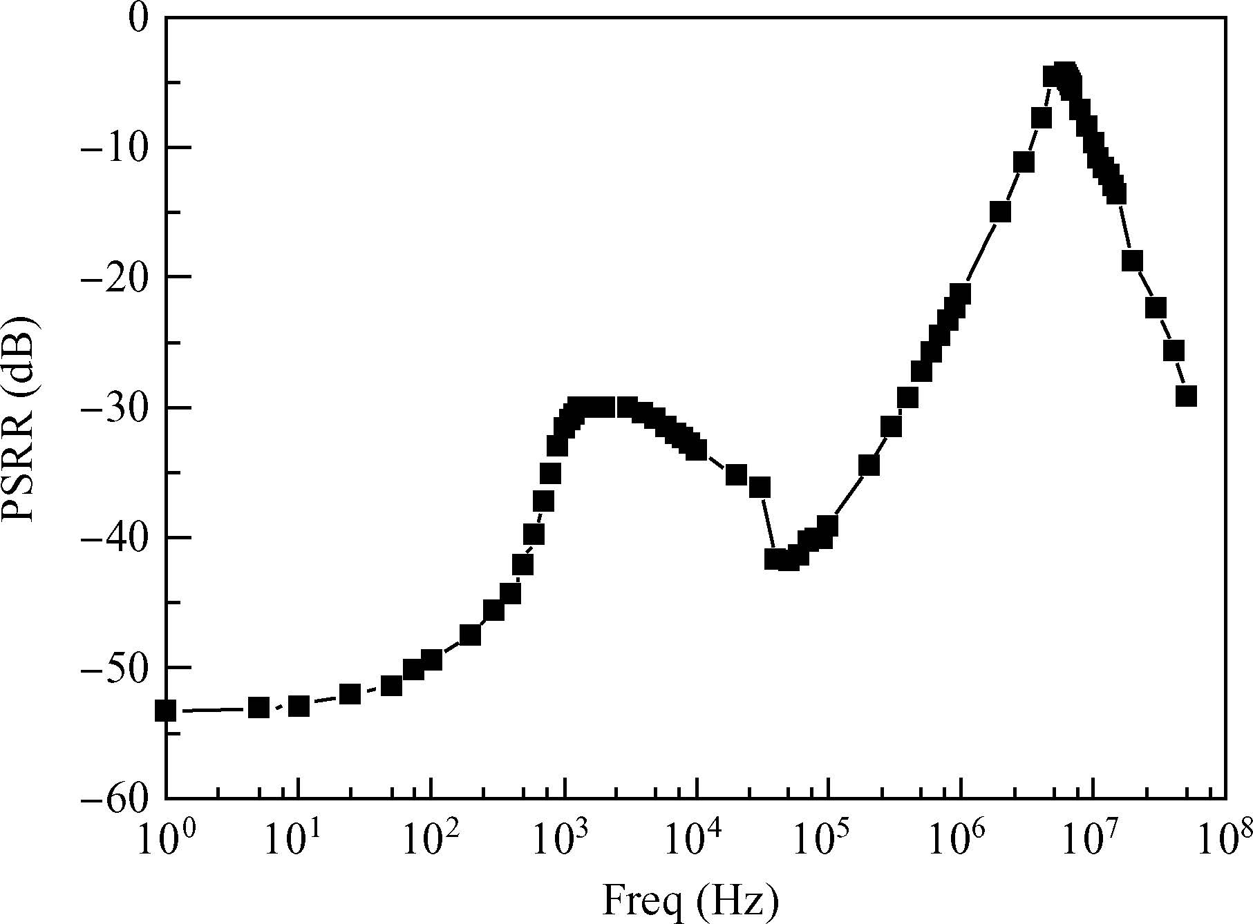
An extremely low power voltage reference without resistors is presented for power-aware ASICs. In order to reduce the power dissipation, an Oguey current reference source is used to reduce the static current; a cascode current mirror is used to increase the power supply rejection ratio (PSRR) and reduce the line sensitivity of the circuit. The voltage reference is fabricated in SMIC 0.18-μm CMOS process. The measured results for the voltage reference demonstrate that the temperature coefficient of the voltage is 66 ppm/℃ in a range from 25 to 100 ℃. The line sensitivity is 0.9% in a supply voltage range of 1.8 to 3.3 V, and PSRR is -49 dB at 100 Hz. The power dissipation is 200 nW. The chip area is 0.01 mm2. The circuit can be used as an elementary circuit block for power-aware ASICs.
J. Semicond.
2015, 36(9): 095007 doi: 10.1088/1674-4926/36/9/095007

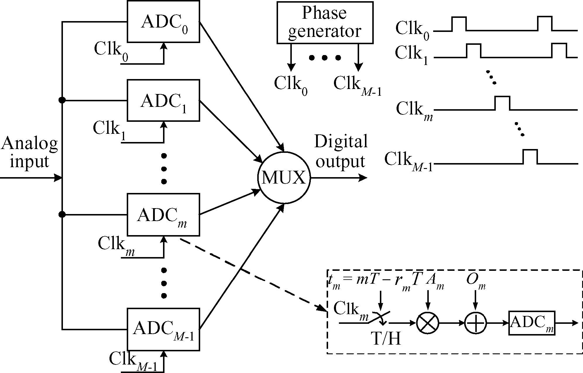
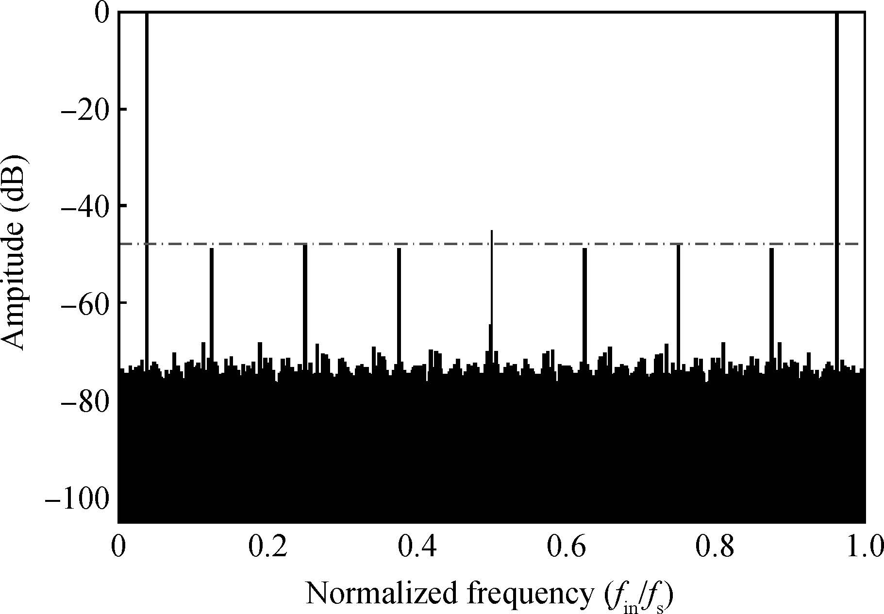
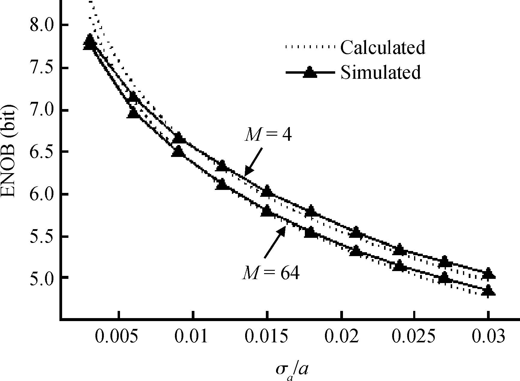
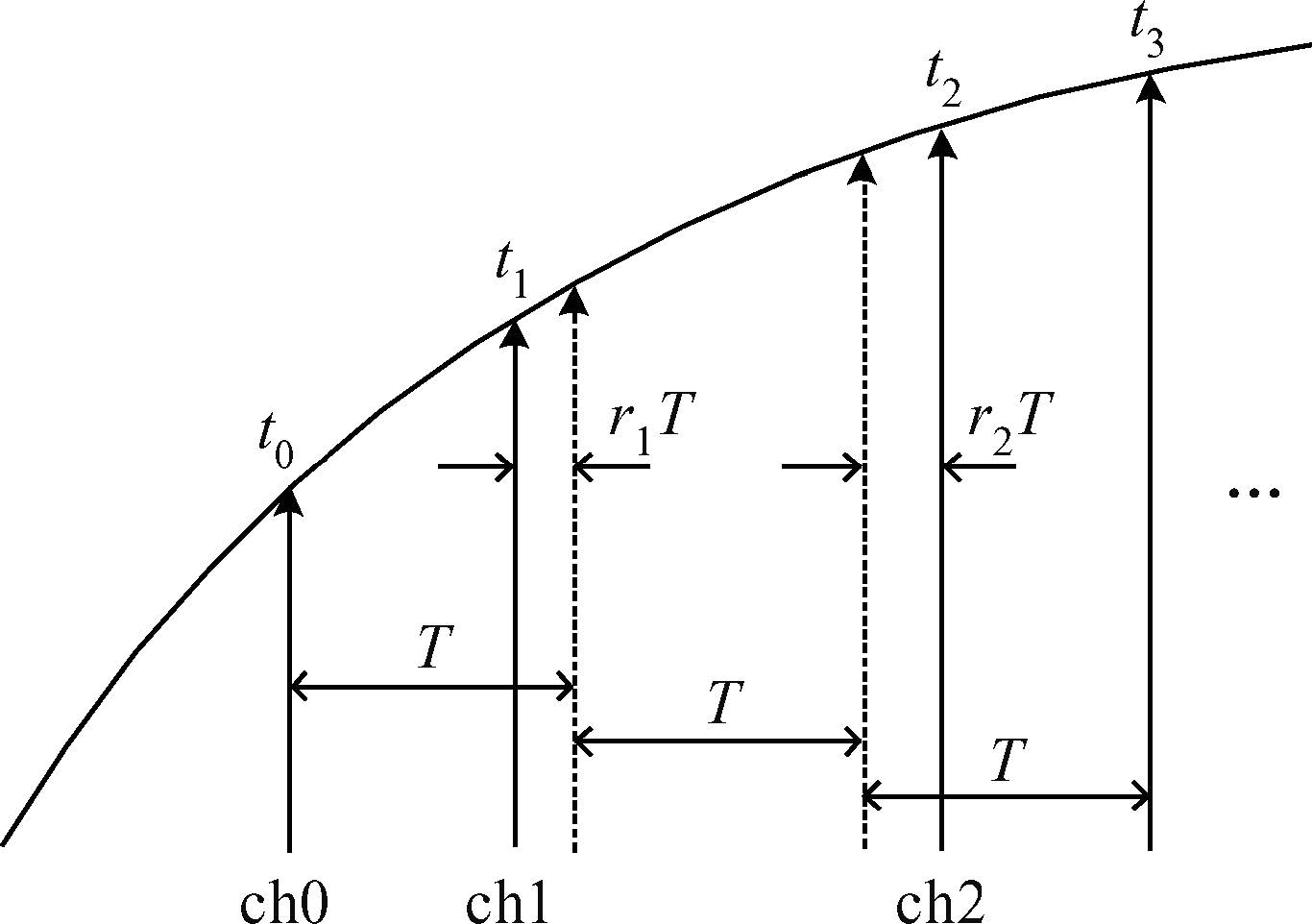
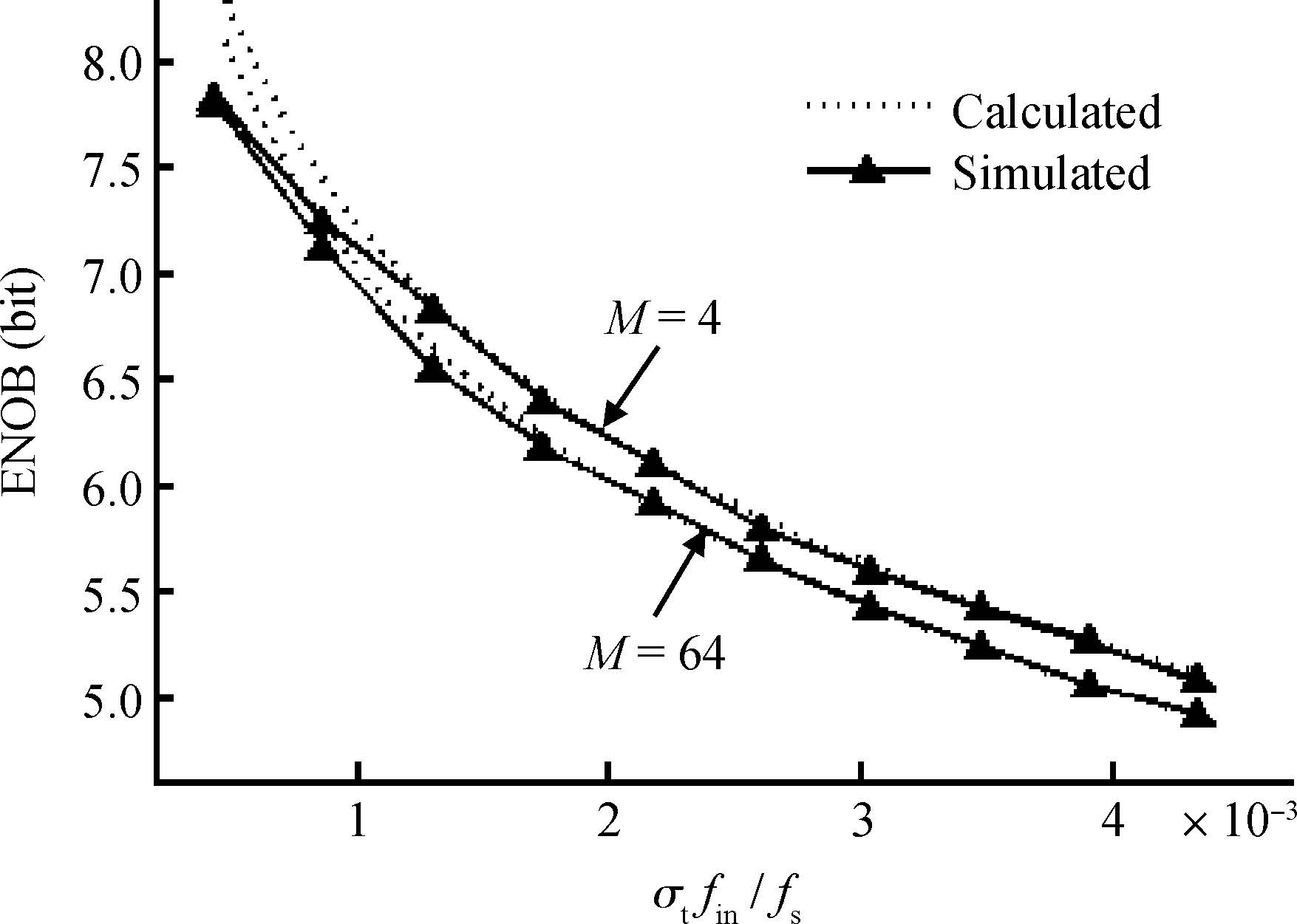
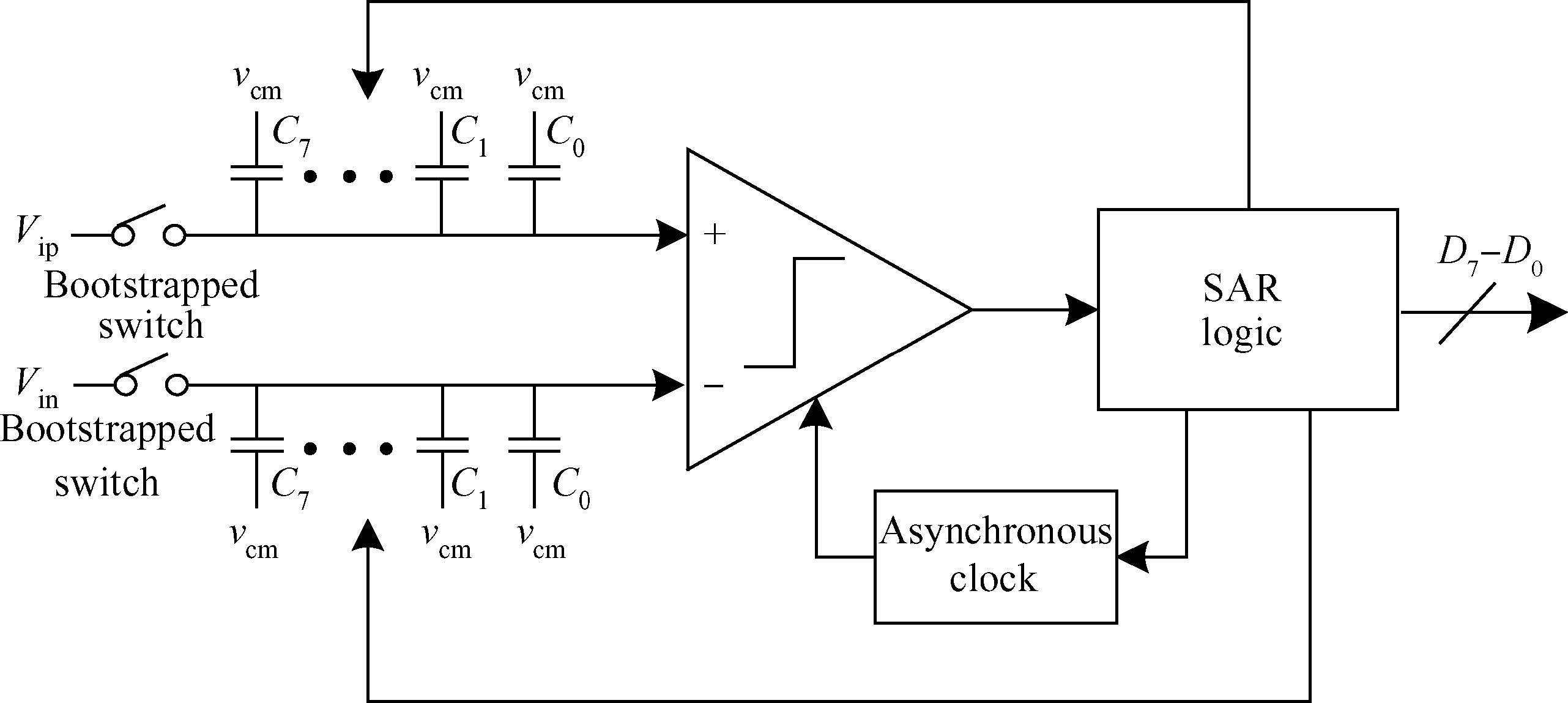
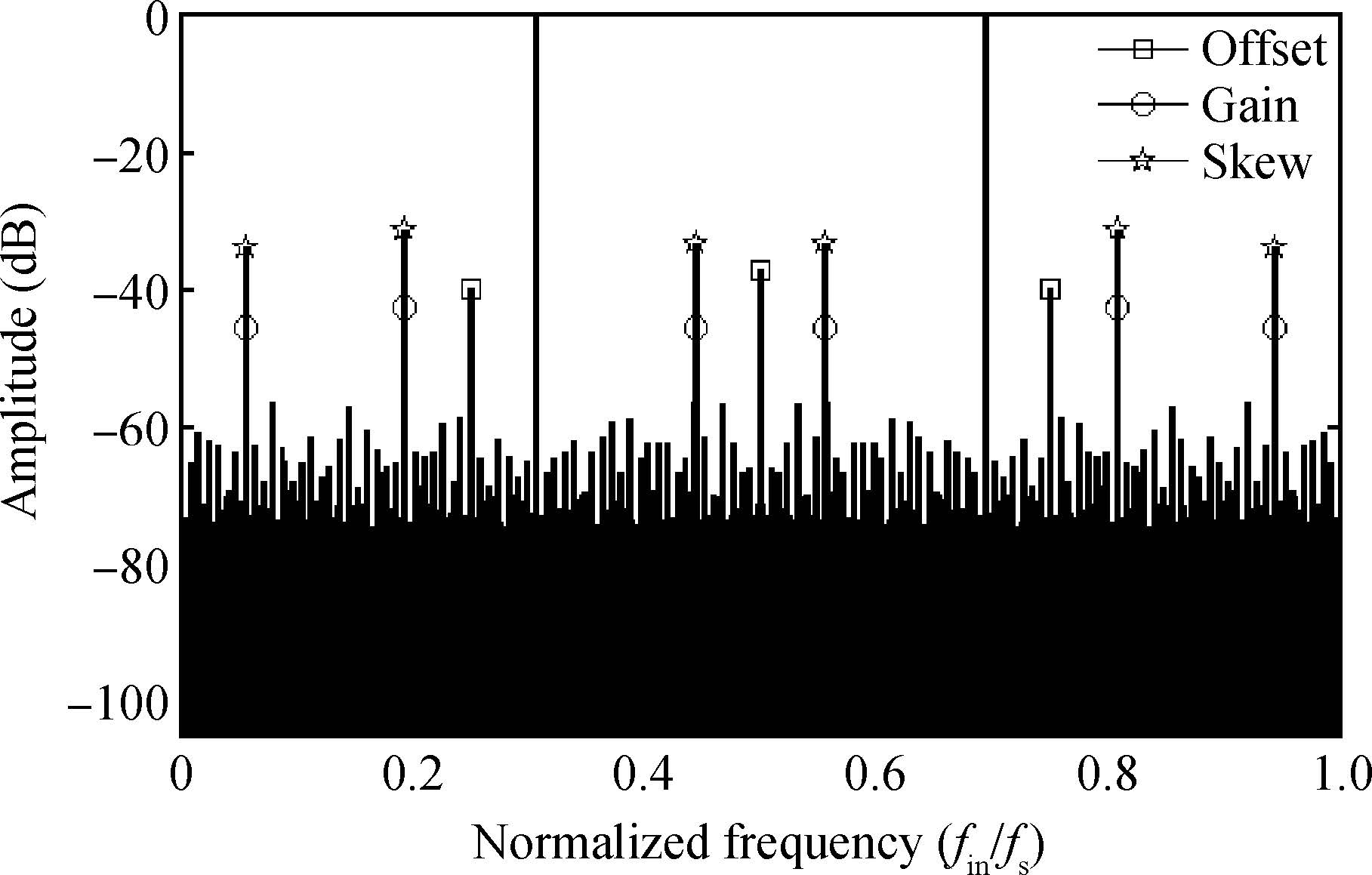
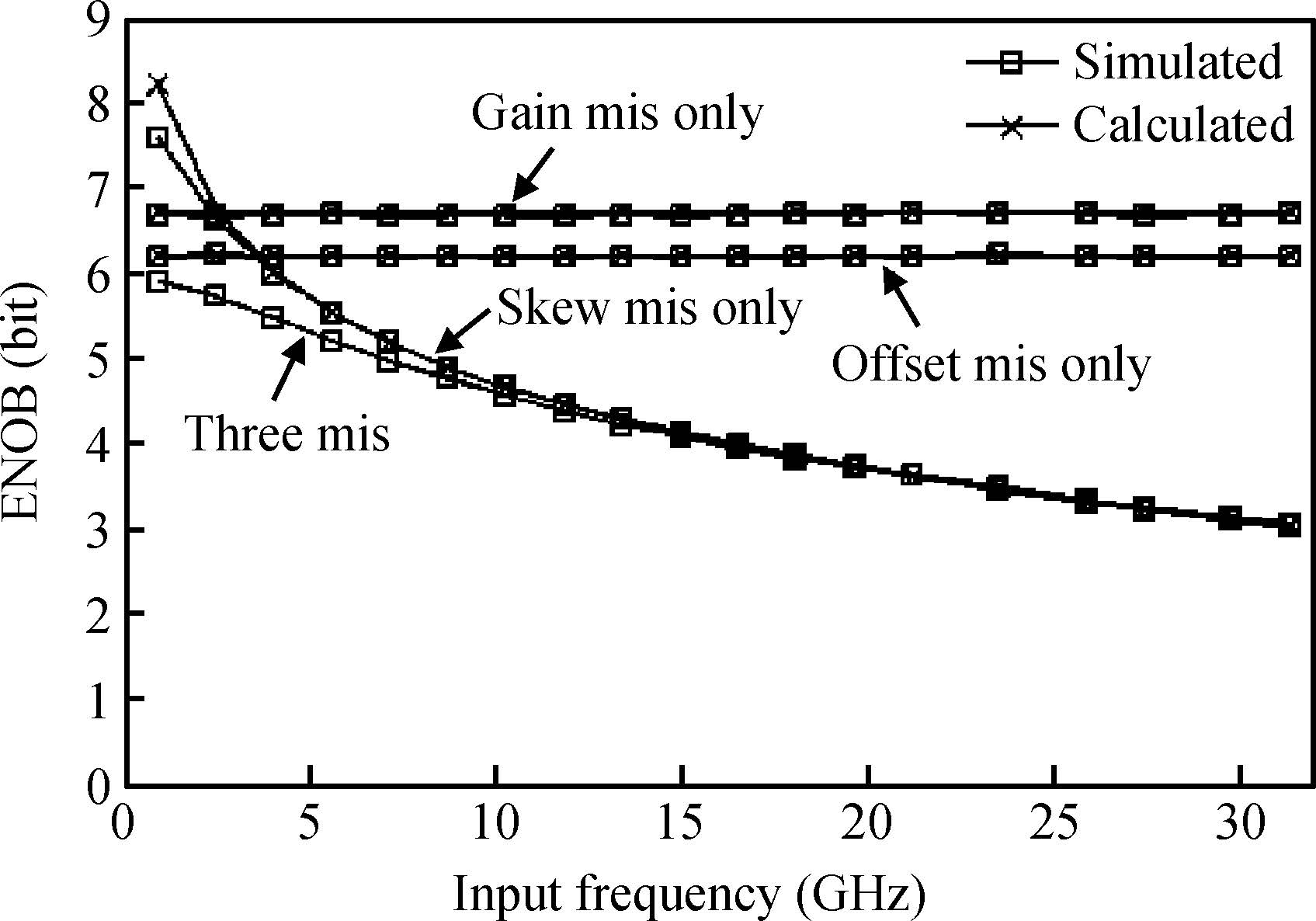
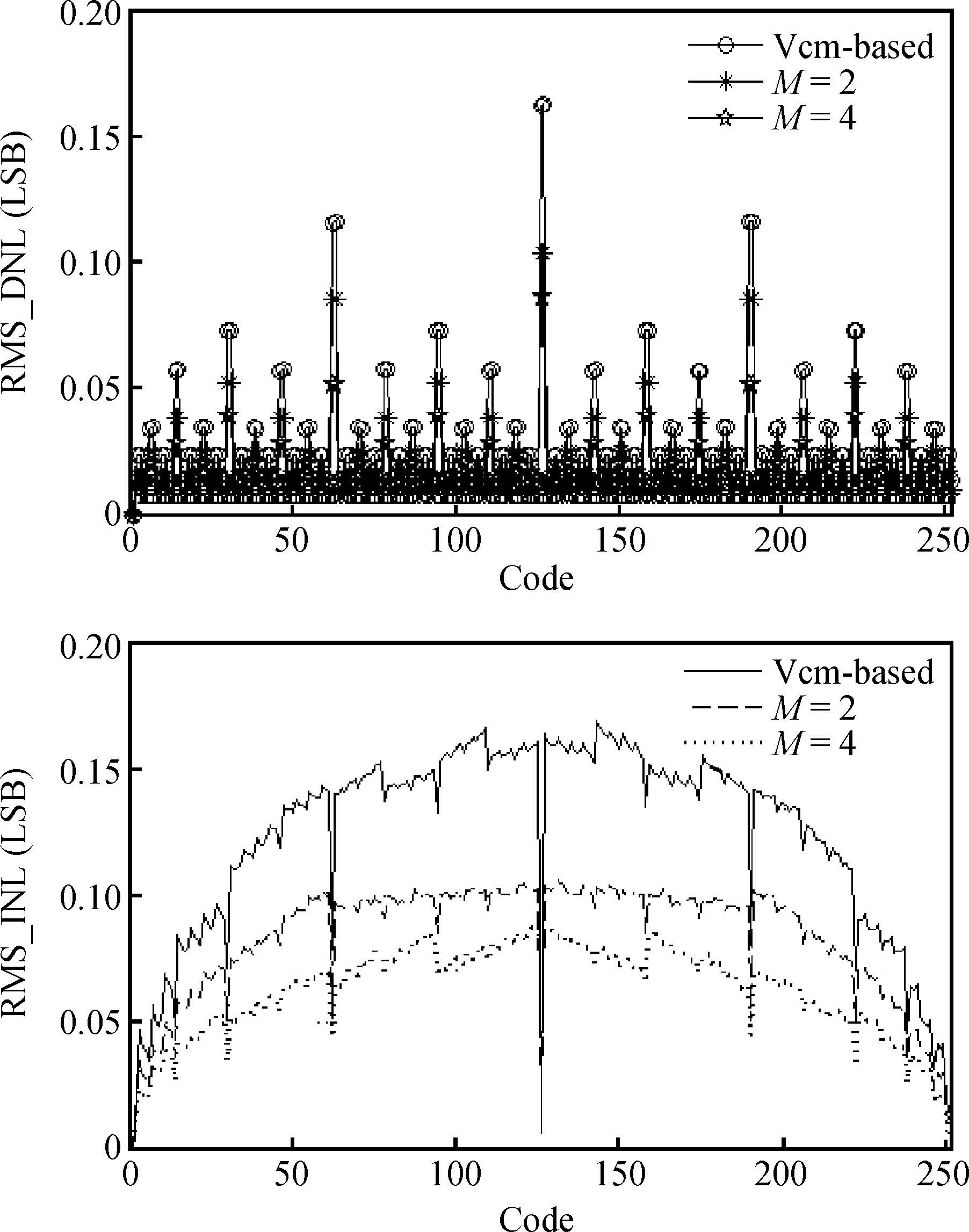
In a time-interleaved analog-to-digital converter (TI ADC), several individual ADCs operate in parallel to achieve a higher sampling rate. Low power consumption as well as good linearity can be obtained by applying successive approximation register (SAR) converters as sub-channel ADCs. In spite of the advantages, this structure suffers from three mismatches, which are offset mismatch, gain mismatch, and time skew. This paper focuses on a TI SAR ADC with a number of channels. The mismatch effects in the frequency domain are analyzed and the derived close form formulas are verified based on Matlab. In addition, we clarify that the standard deviation of DNL and INL of an M-channel TI ADC is reduced by a factor of $\sqrt{M}$ compared to a single channel ADC. The formulas can be used to derive the corresponding requirements when designing a TI ADC. Our analysis process is able to inform the study of calibration algorithms.
J. Semicond.
2015, 36(9): 096001 doi: 10.1088/1674-4926/36/9/096001

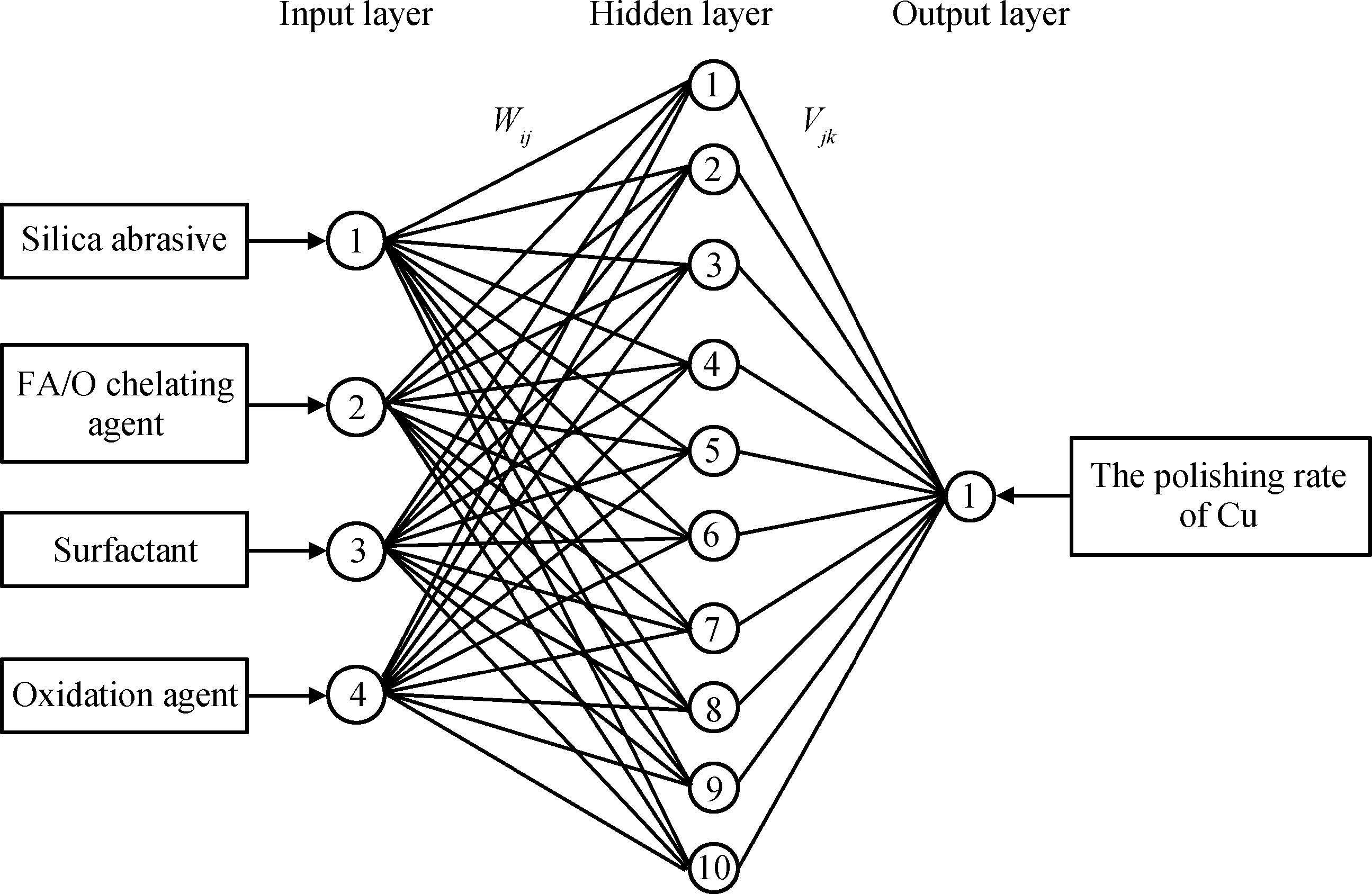
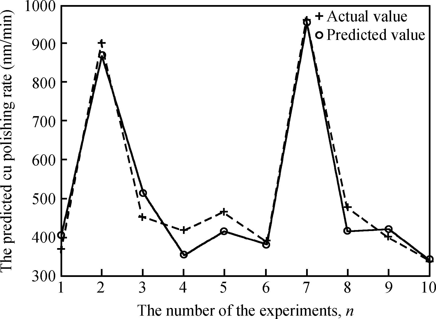
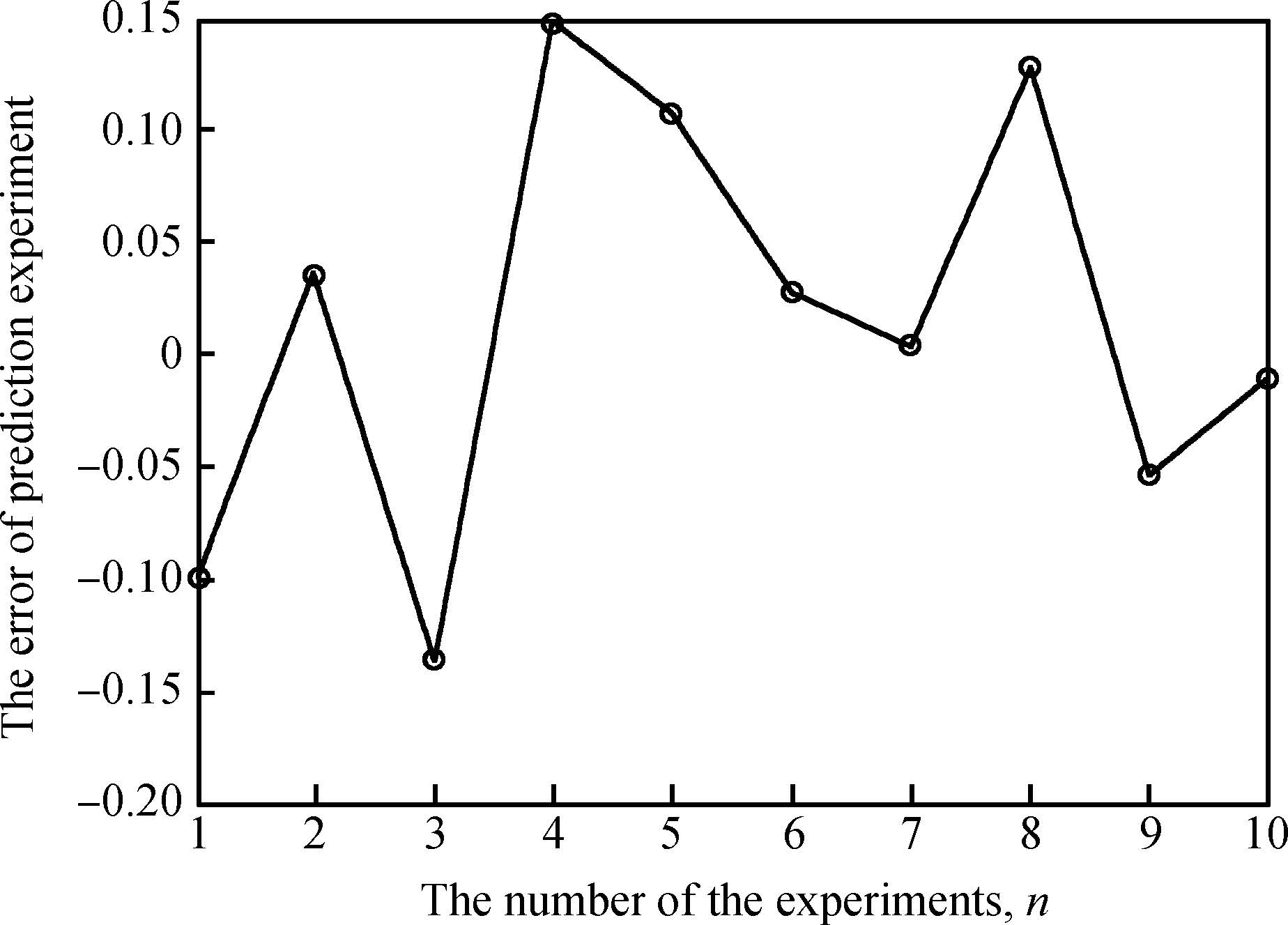
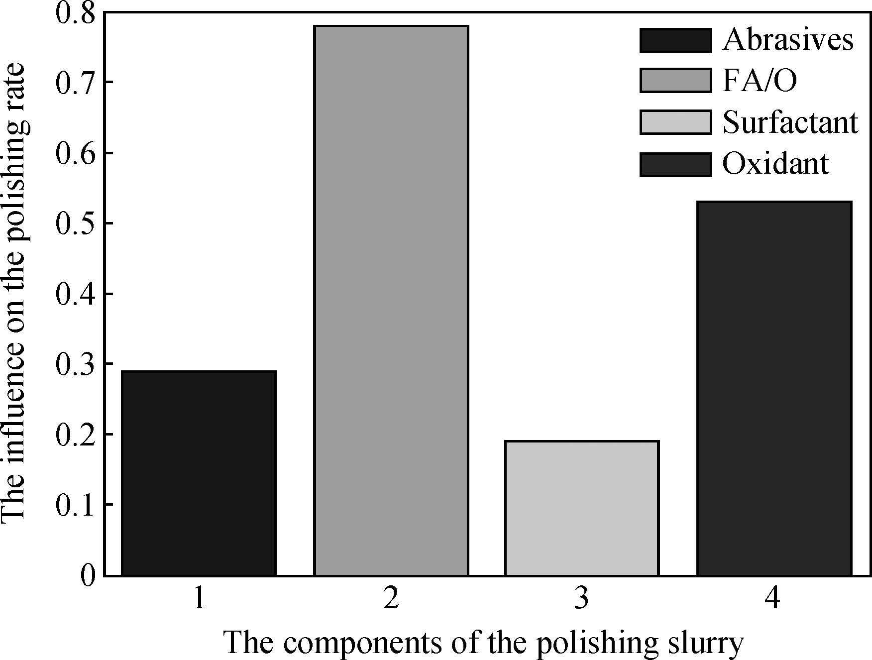
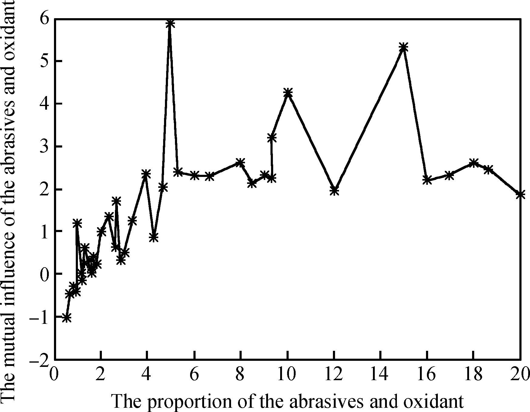
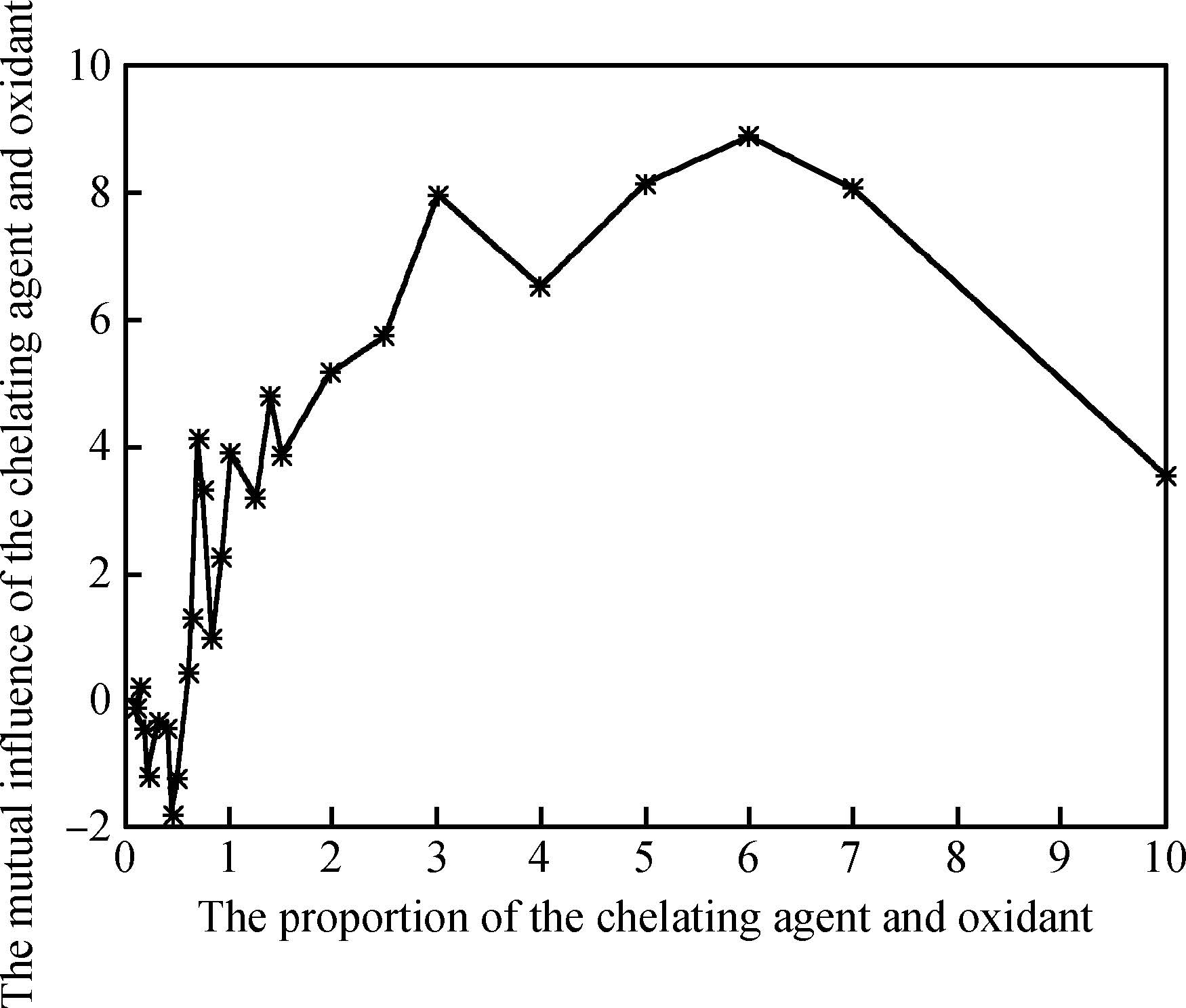
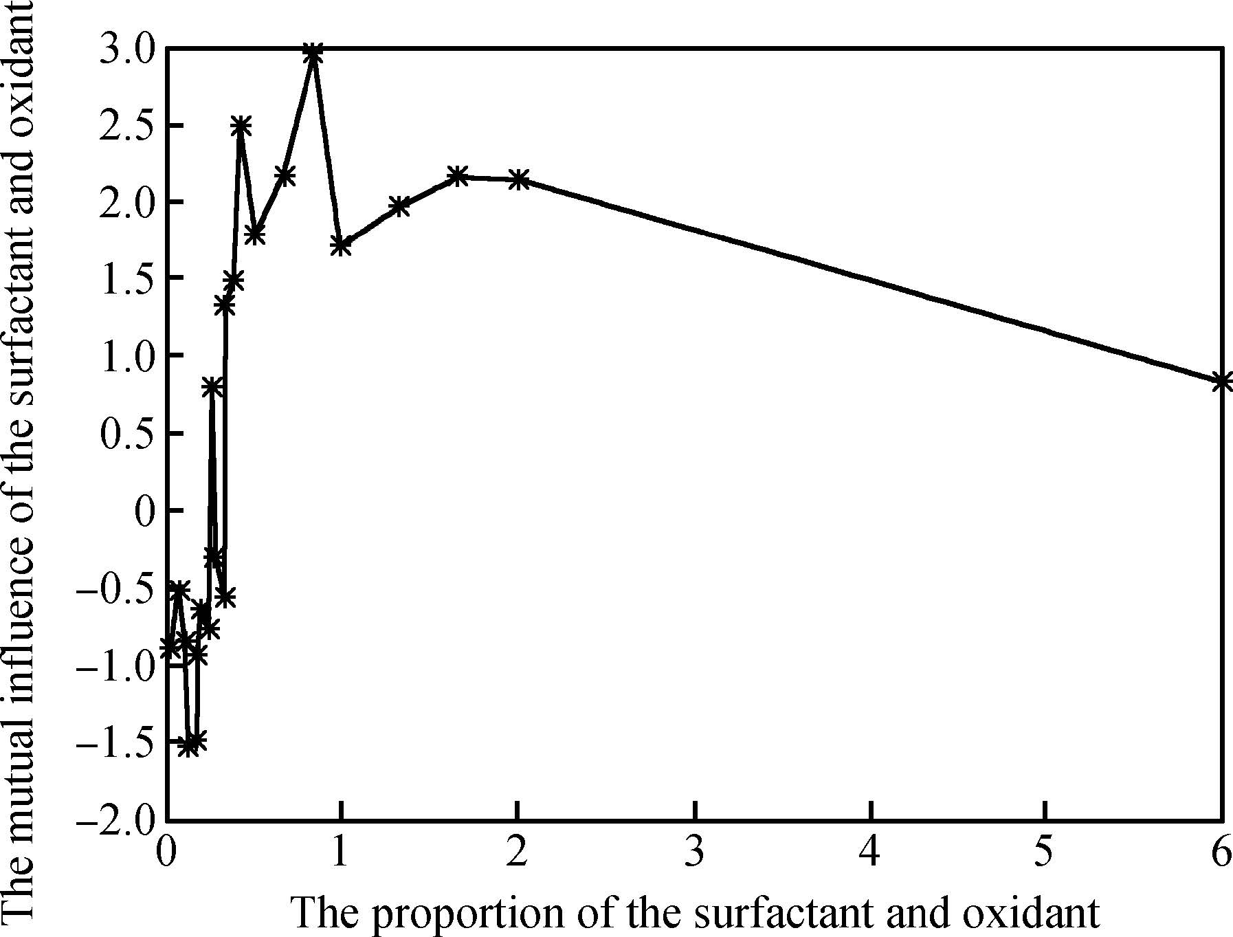
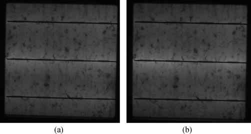
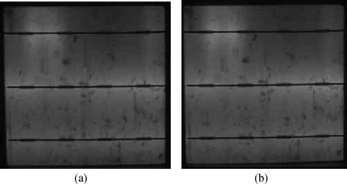
The influence of the components of an alkali polishing slurry and the mutual influences on the Cu polishing rate were investigated by a CMP polishing rate prediction model established with a modified artificial neural network based on the artificial bee colony algorithm. The quantitative method of sensitivity analysis was employed to fulfill the purpose of quantizing the influence on the polishing rate. The result of the analysis indicates that under certain CMP conditions, the Cu polishing rate was controlled by the silica abrasives, the FA/O chelating agent, the surfactant and the oxidant agent in the polishing slurry. Such factors showed the different sensitivity coefficients with 0.78, 0.53, 0.29 and 0.19 respectively on all the sample points. The mutual influence between the FA/O chelating agent and the oxidant agent on the polishing rate seemed obviously strongest when the proportion of them was 2 to 7, with the global sensitivity coefficients between 5 to 9; the mutual influence of silica abrasives and oxidant on the polishing rate was greater as the proportion of the above additives was beyond 5, with the global sensitivity coefficients between 2.5 and 6; the mutual influence of the surfactant and oxidant on the polishing rate was not obvious, with global sensitivity coefficients less than 3. Thus, it provides a kind of effective method for quantitating the influence with the components of the CMP alkali slurry on the polishing rate.