


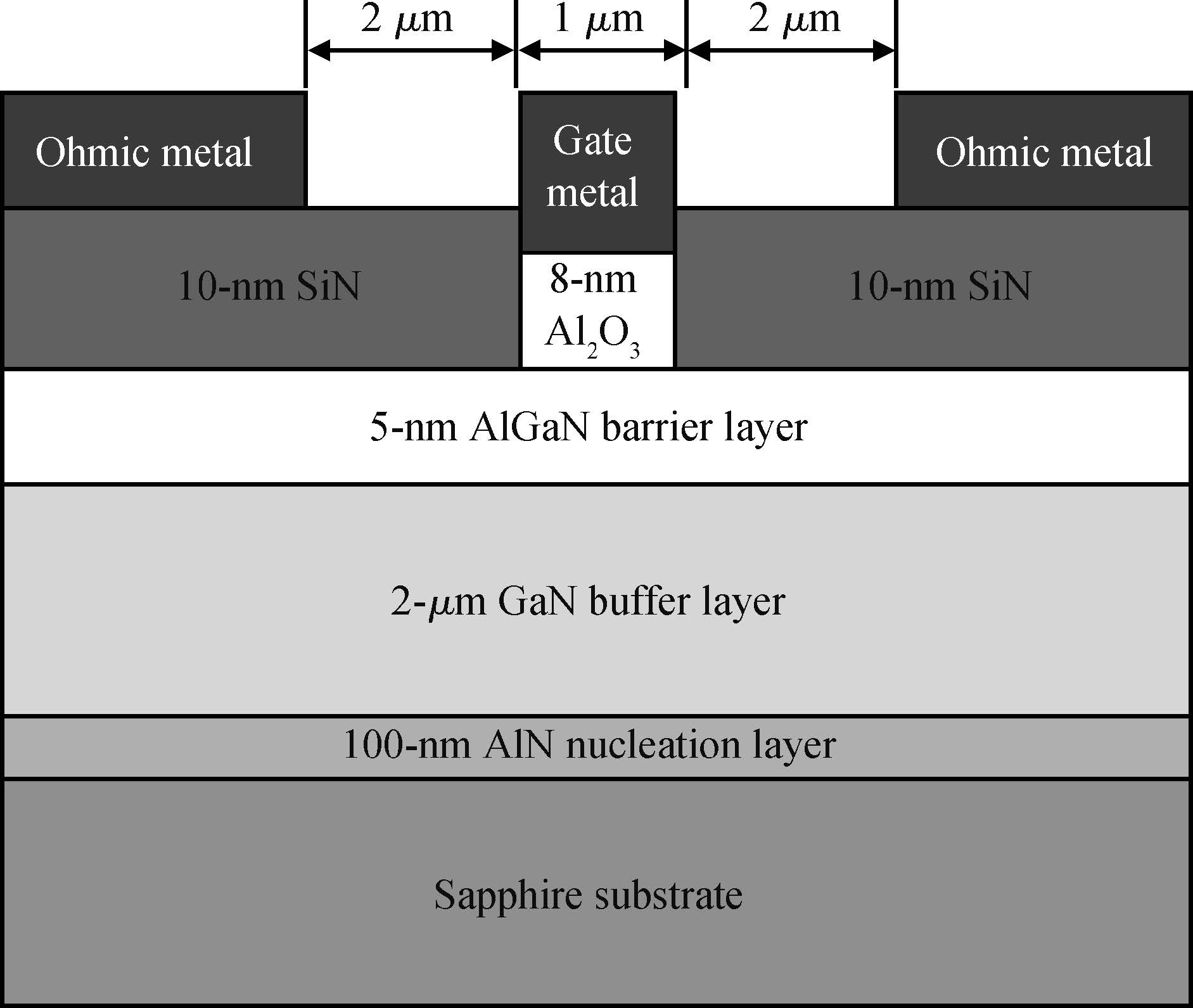
Fig. 1.
Schematic cross-section view of the thin-barrier E-mode AlGaN/GaN MIS-HEMT.
SEMICONDUCTOR DEVICES
Zheli Wang, Jianjun Zhou, Yuechan Kong, Cen Kong, Xun Dong, Yang Yang and Tangsheng Chen
Corresponding author: Wang Zheli, zlwang1990@163.com
Abstract: A high-performance enhancement-mode (E-mode) gallium nitride (GaN)-based metal-insulator-semiconductor high electron mobility transistor (MIS-HEMT) that employs a 5-nm-thick aluminum gallium nitride (Al0.3Ga0.7N) as a barrier layer and relies on silicon nitride (SiN) passivation to control the 2DEG density is presented. Unlike the SiN passivation, aluminum oxide (Al2O3) by atomic layer deposition (ALD) on AlGaN surface would not increase the 2DEG density in the heterointerface. ALD Al2O3 was used as gate insulator after the depletion by etching of the SiN in the gate region. The E-mode MIS-HEMT with gate length (LG) of 1μm showed a maximum drain current density (IDS) of 657 mA/mm, a maximum extrinsic transconductance (gm) of 187 mS/mm and a threshold voltage (Vth) of 1 V. Comparing with the corresponding E-mode HEMT, the device performances had been greatly improved due to the insertion of Al2O3 gate insulator. This provided an excellent way to realize E-mode AlGaN/GaN MIS-HEMTs with both high Vth and IDS.
Keywords: enhancement-mode (E-mode), AlGaN/GaN, metal-insulator-semiconductor high electron mobility transistor (MIS-HEMT), atomic layer deposition (ALD), Al2O3
| [1] | |
| [2] | |
| [3] | |
| [4] | |
| [5] | |
| [6] | |
| [7] | |
| [8] | |
| [9] | |
| [10] | |
| [11] | |
| [12] | |
| [13] | |
| [14] | |
| [15] | |
| [16] |
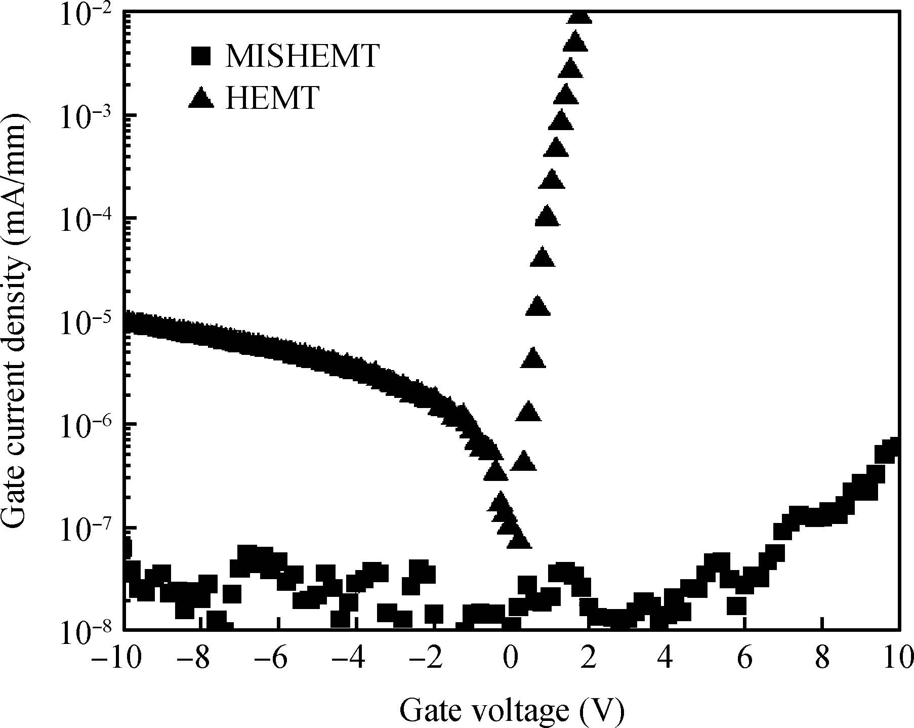
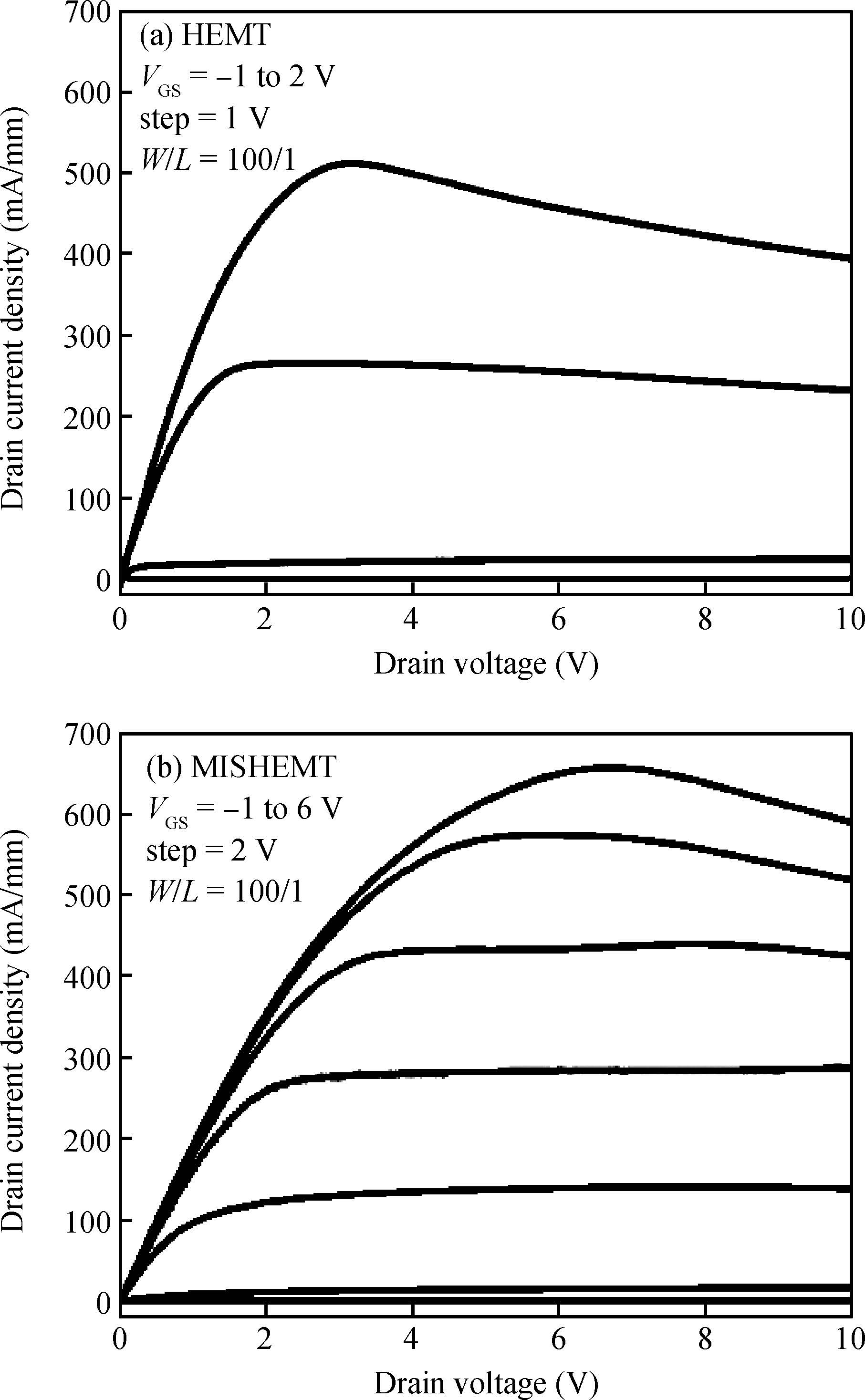
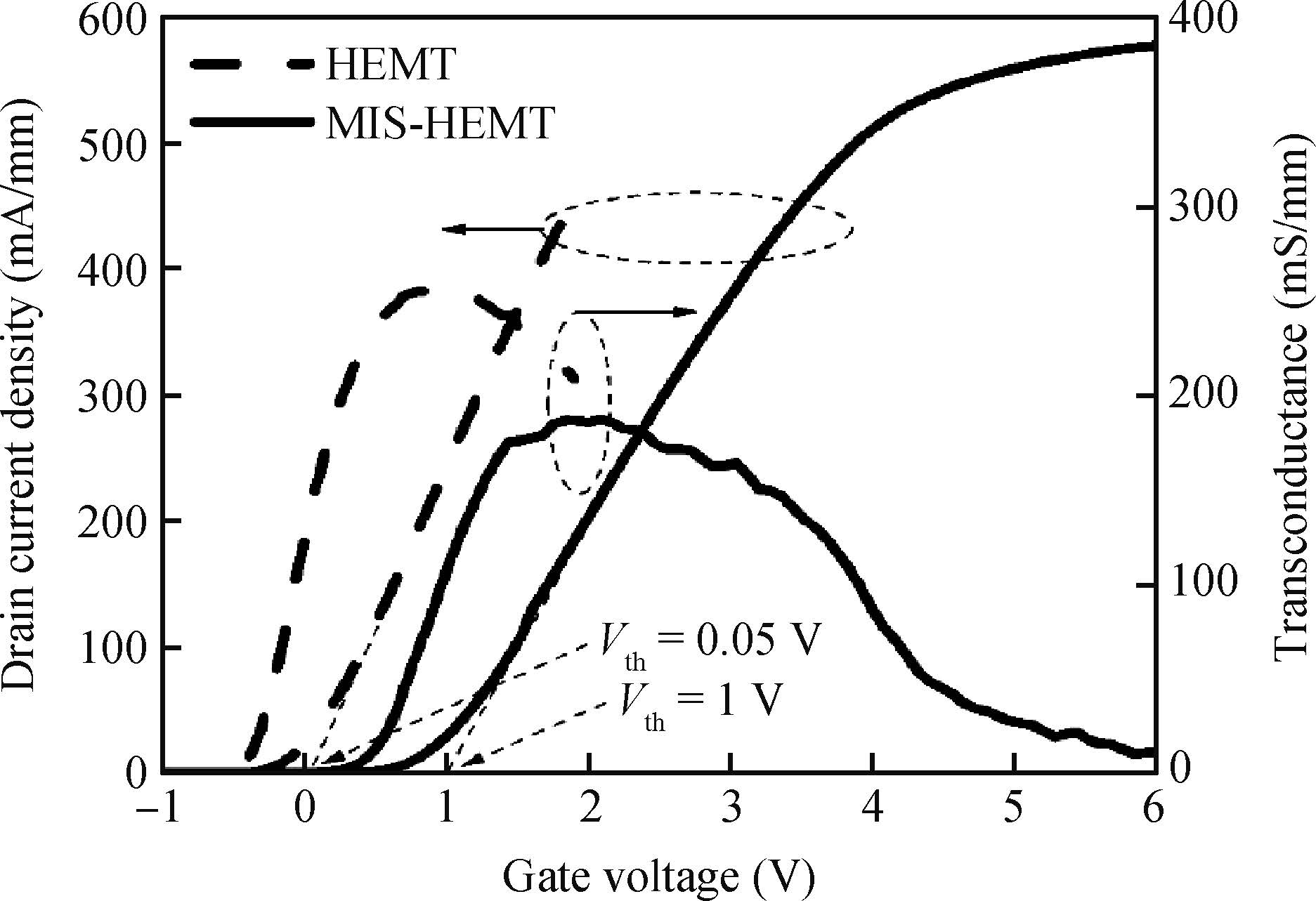
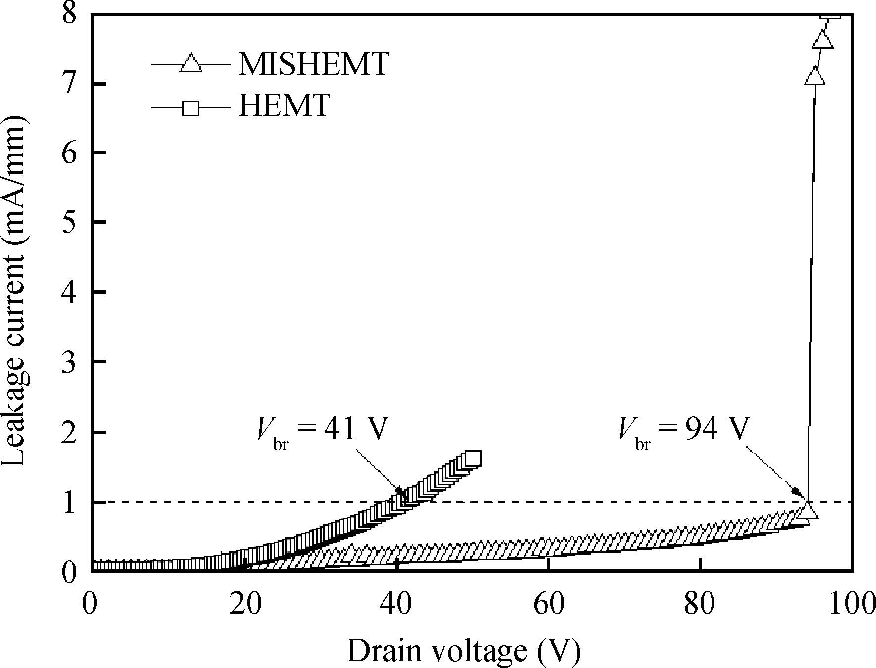
Table 1. Room-temperature Hall measurement before and after the passivation of SiN and Al$_{2}$O$_{3}$ on AlGaN/GaN heterostructure.
 DownLoad: CSV
| [1] | |
| [2] | |
| [3] | |
| [4] | |
| [5] | |
| [6] | |
| [7] | |
| [8] | |
| [9] | |
| [10] | |
| [11] | |
| [12] | |
| [13] | |
| [14] | |
| [15] | |
| [16] |


Article views: 4498 Times PDF downloads: 114 Times Cited by: 0 Times
Received: 09 March 2015 Revised: Online: Published: 01 September 2015
| Citation: |
Zheli Wang, Jianjun Zhou, Yuechan Kong, Cen Kong, Xun Dong, Yang Yang, Tangsheng Chen. Thin-barrier enhancement-mode AlGaN/GaN MIS-HEMT using ALD Al2O3 as gate insulator[J]. Journal of Semiconductors, 2015, 36(9): 094004. doi: 10.1088/1674-4926/36/9/094004
****
Z L Wang, J J Zhou, Y C Kong, C Kong, X Dong, Y Yang, T S Chen. Thin-barrier enhancement-mode AlGaN/GaN MIS-HEMT using ALD Al2O3 as gate insulator[J]. J. Semicond., 2015, 36(9): 094004. doi: 10.1088/1674-4926/36/9/094004.

|
| [1] | |
| [2] | |
| [3] | |
| [4] | |
| [5] | |
| [6] | |
| [7] | |
| [8] | |
| [9] | |
| [10] | |
| [11] | |
| [12] | |
| [13] | |
| [14] | |
| [15] | |
| [16] |

 WeChat ID
Journal of Semiconductors © 2017 All Rights Reserved 京ICP备05085259号-2


