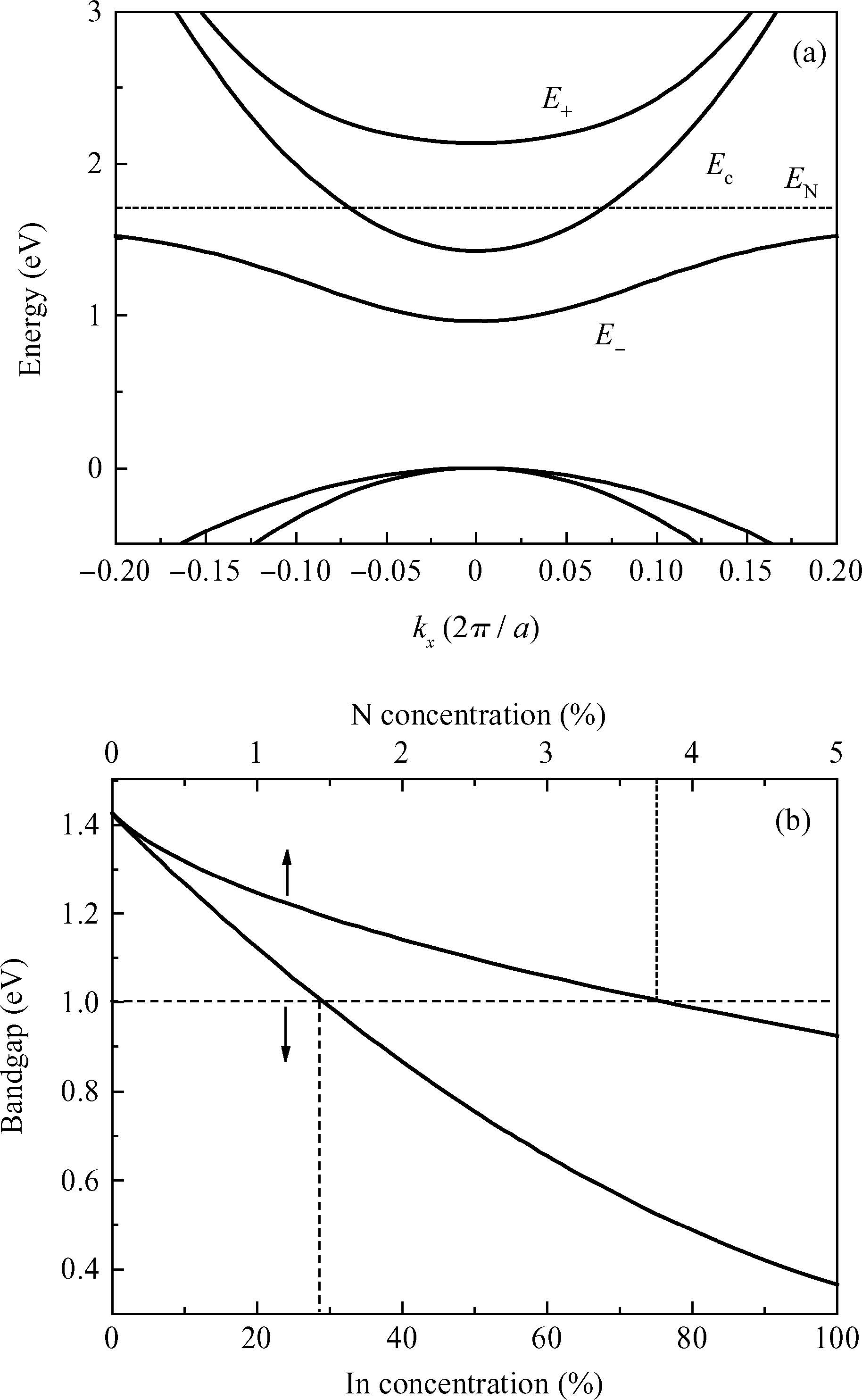
图 1.
Schematic of BAC model and bandgap diagram. (a)
Schematic band diagram of GaN0:045As. (b) Bandgap of GaNAs and
GaInAs as a function of N/In concentration.
SEMICONDUCTOR DEVICES
Haixiao Wang1, Xinhe Zheng1, 2, , Xinyuan Gan1, Naiming Wang1 and Hui Yang1
Corresponding author: Xinhe Zheng, Email: xinhezheng@ustb.edu.cn, xhzheng2009@sinano.ac.cn
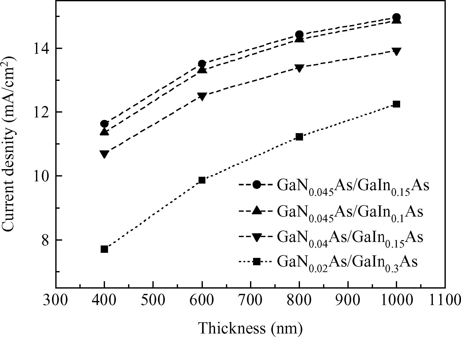
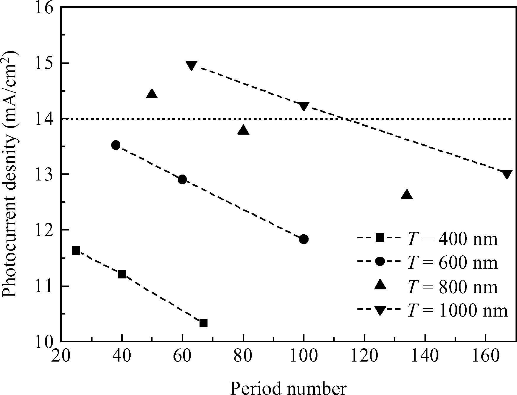
Abstract: A reasonably-thick GaNAs/GaInAs superlattice could be an option as a roughly 1 eV subcell to achieve high-efficiency multi-junction solar cells on a lattice-matched Ge substrate. A detailed consideration of a high-efficiency design for a GaInP/GaAs/1 eV/Ge device is presented. Calculations have been done for this structure to obtain the confined energies of the electrons and holes by utilizing the Kronig-Penney model, as well as the absorption coefficient and thereby the external quantum efficiency. The effect of well layers, GaNAs or GaInAs, on the absorption and photocurrent density under the AM 1.5 condition is discussed in order to realize a requirement of current matching in the four-junction solar cells. The management of these considerations implies the feasibility of the GaNAs/GaInAs superlattice subcell design to improve the overall conversion efficiency of lattice matched GaInP/GaAs/1 eV/Ge cells.
Keywords: superlattice, theoretical designing, solar cell, current match
| [1] | |
| [2] | |
| [3] | |
| [4] | |
| [5] | |
| [6] | |
| [7] | |
| [8] | |
| [9] | |
| [10] | |
| [11] | |
| [12] | |
| [13] | |
| [14] | |
| [15] | |
| [16] | |
| [17] | |
| [18] | |
| [19] | |
| [20] | |
| [21] |
| [1] | |
| [2] | |
| [3] | |
| [4] | |
| [5] | |
| [6] | |
| [7] | |
| [8] | |
| [9] | |
| [10] | |
| [11] | |
| [12] | |
| [13] | |
| [14] | |
| [15] | |
| [16] | |
| [17] | |
| [18] | |
| [19] | |
| [20] | |
| [21] |


Article views: 3756 Times PDF downloads: 18 Times Cited by: 0 Times
Received: 27 March 2015 Revised: Online: Published: 01 January 2016
| Citation: |
Haixiao Wang, Xinhe Zheng, Xinyuan Gan, Naiming Wang, Hui Yang. Designing of 1 eV GaNAs/GaInAs superlattice subcell in current-matched four-junction solar cell[J]. Journal of Semiconductors, 2016, 37(1): 014004. doi: 10.1088/1674-4926/37/1/014004
****
H X Wang, X H Zheng, X Y Gan, N M Wang, H Yang. Designing of 1 eV GaNAs/GaInAs superlattice subcell in current-matched four-junction solar cell[J]. J. Semicond., 2016, 37(1): 014004. doi: 10.1088/1674-4926/37/1/014004.

|
| [1] | |
| [2] | |
| [3] | |
| [4] | |
| [5] | |
| [6] | |
| [7] | |
| [8] | |
| [9] | |
| [10] | |
| [11] | |
| [12] | |
| [13] | |
| [14] | |
| [15] | |
| [16] | |
| [17] | |
| [18] | |
| [19] | |
| [20] | |
| [21] |

 WeChat ID
Journal of Semiconductors © 2017 All Rights Reserved 京ICP备05085259号-2

 DownLoad: