J. Semicond. > 2016, Volume 37 > Issue 1 > 015004

SEMICONDUCTOR INTEGRATED CIRCUITS

A 10 bit 50 MS/s SAR ADC with partial split capacitor switching scheme in 0.18 μm CMOS

Dong Li, Qiao Meng and Fei Li

+ Author Affiliations

 Corresponding author: Meng Qiao,Email:mengqiao@seu.edu.cn

DOI: 10.1088/1674-4926/37/1/015004

PDF

Abstract: This paper presents a 10 bit successive approximation register (SAR) analog-to-digital converter (ADC) in 0.18 μ m 1P6M CMOS technology with a 1.8 V supply voltage. To improve the conversion speed, a partial split capacitor switching scheme is proposed. By reducing the time constant of the bit cycles, the proposed technique shortens the settling time of a capacitive digital-to-analog converter (DAC). In addition, a new SAR control logic is proposed to reduce loop delay to further enhance the conversion speed. At 1.8 V supply voltage and 50 MS/s the SAR ADC achieves a signal-to-noise and distortion ratio (SNDR) of 57.5 dB and spurious-free dynamic range (SFDR) of 69.3 dB. The power consumption is 2.26 mW and the core die area is 0.096 mm2.

Key words: SAR ADCswitching schemeSAR control logicDACcomparator


[1]
[2]
[3]
[4]
[5]
[6]
[7]
[8]
[9]
[10]
[11]
[12]
[13]
[14]
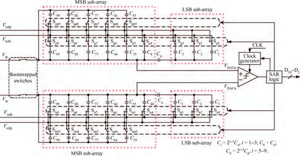
Fig. 1.  Block diagram of the proposed fully differential SAR ADC.

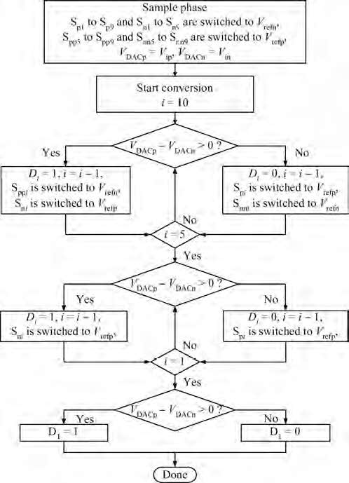
Fig. 2.  Flow chart of the proposed switching scheme.

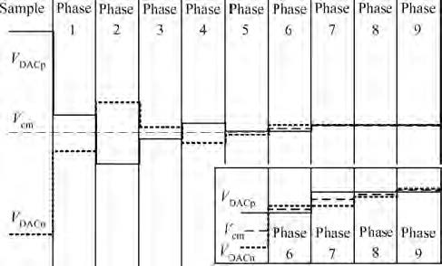
Fig. 3.  Output waveform of the proposed switching method.

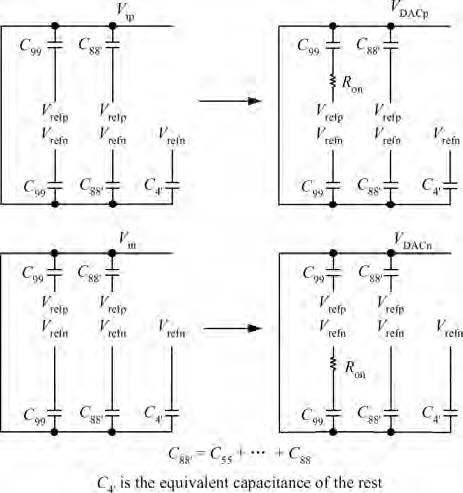
Fig. 4.  Equivalent circuit of the longest settling procedure of the proposed switching scheme.

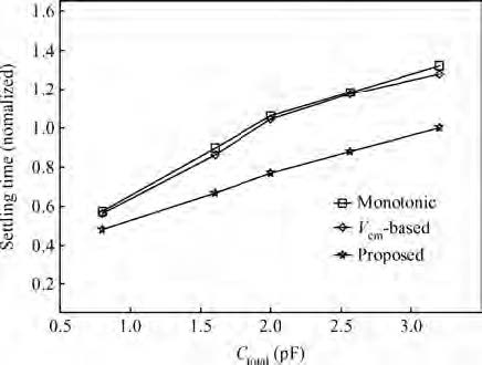
Fig. 5.  The settling time against total capacitance of DAC.

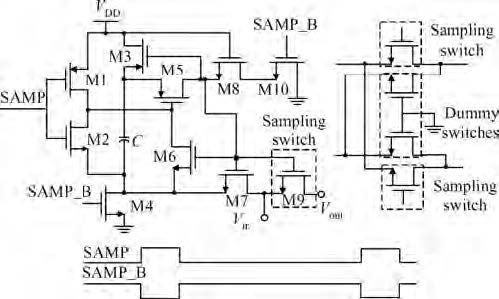
Fig. 6.  Schematic of the bootstrapped switch.

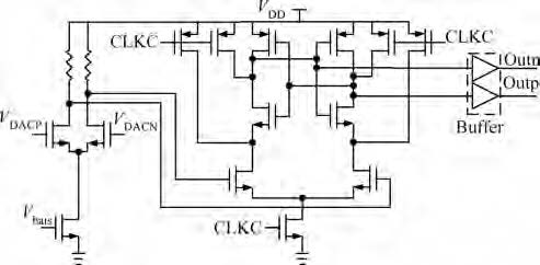
Fig. 7.  Schematic of the dynamic comparator with pre-amplifier.

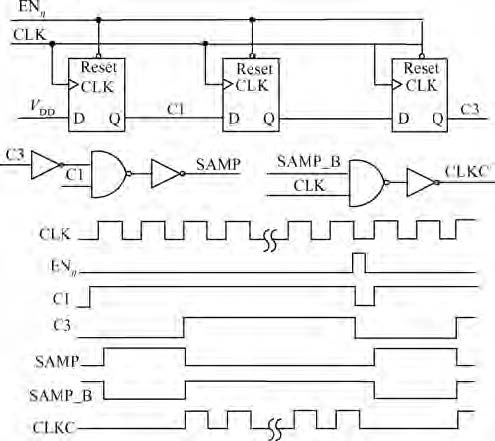
Fig. 8.  Schematic and timing diagram of the synchronous clock generator.

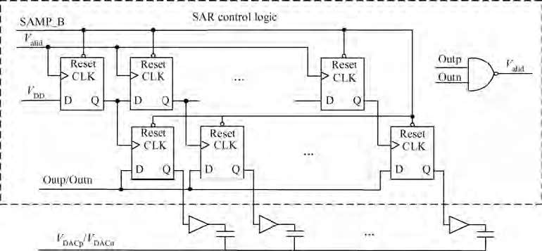
Fig. 9.  Diagram of the conventional SAR logic.

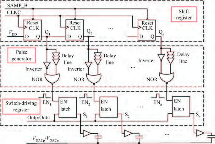
Fig. 10.  Diagram of the proposed SAR logic.

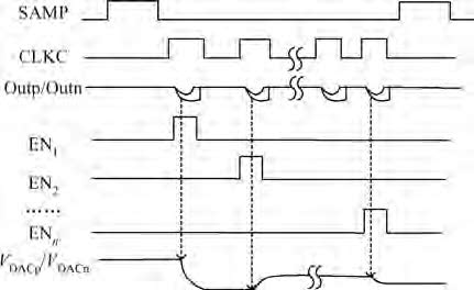
Fig. 11.  Timing diagram of the principle of the proposed SAR control logic.

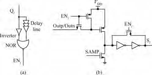
Fig. 12.  Schematics of (a) the pulse generator and (b) the latch.

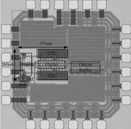
Fig. 13.  Chip microphotograph.

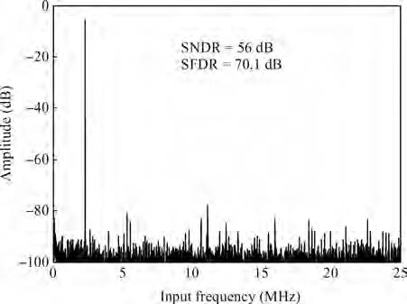
Fig. 14.  Measured FFT spectrum at 50 MS/s and 2.02 MHz input.

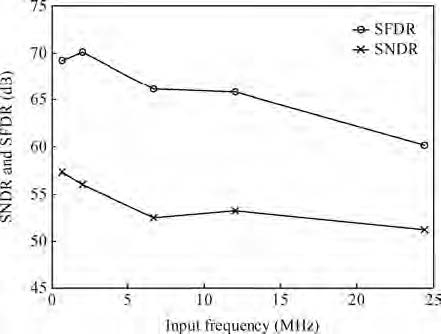
Fig. 15.  Dynamic performance versus input frequency.

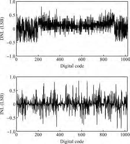
Fig. 16.  Measured DNL and INL.

Table 1.   Performance summary.

DownLoad: CSV

Table 2.   Comparison with state-of-the-other-art works.

DownLoad: CSV
[1]
[2]
[3]
[4]
[5]
[6]
[7]
[8]
[9]
[10]
[11]
[12]
[13]
[14]
1

Inhomogeneous barrier height effect on the current-voltage characteristics of an Au/n-InP Schottky diode

Kamal Zeghdar, Lakhdar Dehimi, Achour Saadoune, Nouredine Sengouga

Journal of Semiconductors, 2015, 36(12): 124002. doi: 10.1088/1674-4926/36/12/124002

2

Backgating effect in GaAs FETs with a channel-semi-insulating substrate boundary

Ahmed Chaouki Megherbi, Said Benramache, Abderrazak Guettaf

Journal of Semiconductors, 2014, 35(3): 034004. doi: 10.1088/1674-4926/35/3/034004

3

Dynamic threshold voltage operation in Si and SiGe source junctionless tunnel field effect transistor

Shibir Basak, Pranav Kumar Asthana, Yogesh Goswami, Bahniman Ghosh

Journal of Semiconductors, 2014, 35(11): 114001. doi: 10.1088/1674-4926/35/11/114001

4

Pinch-off voltage modeling for CMOS image pixels with a pinned photodiode structure

Chen Cao, Bing Zhang, Longsheng Wu, Xin Li, Junfeng Wang, et al.

Journal of Semiconductors, 2014, 35(7): 074012. doi: 10.1088/1674-4926/35/7/074012

5

MOS Capacitance–Voltage Characteristics: IV. Trapping Capacitance from 3-Charge-State Impurities

Jie Binbin, Sah Chihtang

Journal of Semiconductors, 2012, 33(1): 011001. doi: 10.1088/1674-4926/33/1/011001

6

MOS Capacitance-Voltage Characteristics: V. Methods to Enhance the Trapping Capacitance

Jie Binbin, Sah Chihtang

Journal of Semiconductors, 2012, 33(2): 021001. doi: 10.1088/1674-4926/33/2/021001

7

MOS Capacitance-Voltage Characteristics II. Sensitivity of Electronic Trapping at Dopant Impurity from Parameter Variations

Jie Binbin, Sah Chihtang

Journal of Semiconductors, 2011, 32(12): 121001. doi: 10.1088/1674-4926/32/12/121001

8

A low-voltage low-power CMOS voltage reference based on subthreshold MOSFETs

Wang Honglai, Zhang Xiaoxing, Dai Yujie, Lü Yingjie, Toshimasa Matsuoka, et al.

Journal of Semiconductors, 2011, 32(8): 085009. doi: 10.1088/1674-4926/32/8/085009

9

MOS Capacitance–Voltage Characteristics from Electron-Trapping at Dopant Donor Impurity

Jie Binbin, Sah Chihtang

Journal of Semiconductors, 2011, 32(4): 041001. doi: 10.1088/1674-4926/32/4/041001

10

MOS Capacitance-Voltage Characteristics III. Trapping Capacitance from 2-Charge-State Impurities

Jie Binbin, Sah Chihtang

Journal of Semiconductors, 2011, 32(12): 121002. doi: 10.1088/1674-4926/32/12/121002

11

A novel complementary N+-charge island SOI high voltage device

Wu Lijuan, Hu Shengdong, Zhang Bo, Li Zhaoji

Journal of Semiconductors, 2010, 31(11): 114010. doi: 10.1088/1674-4926/31/11/114010

12

Low voltage bandgap reference with closed loop curvature compensation

Fan Tao, Du Bo, Zhang Zheng, Yuan Guoshun

Journal of Semiconductors, 2009, 30(3): 035006. doi: 10.1088/1674-4926/30/3/035006

13

A novel on-chip high to low voltage power conversion circuit

Wang Hui, Wang Songlin, Lai Xinquan, Ye Qiang, Mou Zaixin, et al.

Journal of Semiconductors, 2009, 30(3): 035008. doi: 10.1088/1674-4926/30/3/035008

14

Silicide-block-film effects on high voltage drain-extended MOS transistors

Wang Lei, Gao Chao, Liu Bo, Hu Jian, Lee Po, et al.

Journal of Semiconductors, 2009, 30(3): 034003. doi: 10.1088/1674-4926/30/3/034003

15

Capacitance–voltage characterization of fully silicided gated MOS capacitor

Wang Baomin, Ru Guoping, Jiang Yulong, Qu Xinping, Li Bingzong, et al.

Journal of Semiconductors, 2009, 30(3): 034002. doi: 10.1088/1674-4926/30/3/034002

16

Axial Local Lifetime Control in High-Voltage Diodes Based on Proximity Gettering of Platinum by Proton-Implantation Damages

Jia Yunpeng, Zhang Bin, Sun Yuechen, Kang Baowei

Chinese Journal of Semiconductors , 2006, 27(2): 294-297.

17

Low Voltage Flash Memory Cells Using SiGe Quantum Dots for Enhancing F-N Tunneling

Deng Ning, Pan Liyang, Liu Zhihong, Zhu Jun, Chen Peiyi, et al.

Chinese Journal of Semiconductors , 2006, 27(3): 454-458.

18

Breakdown Voltage and Charge to Breakdown Investigation of Gate Oxide of 0.18μm Dual Gate CMOS Process with Different Measurement Methods

Zhao Yi, Wan Xinggong, Xu Xiangming, Cao Gang, Bu Jiao, et al.

Chinese Journal of Semiconductors , 2006, 27(2): 290-293.

19

Sub-1V CMOS Voltage Reference Based on Weighted Vgs

Zhang Xun, Wang Peng, Jin Dongming

Chinese Journal of Semiconductors , 2006, 27(5): 774-777.

20

On-State Breakdown Model for High Voltage RESURF LDMOS

Fang Jian, Yi Kun, Li Zhaoji, and Zhang Bo(436)

Chinese Journal of Semiconductors , 2005, 26(3): 436-442.

  • Search

    Advanced Search >>

    GET CITATION

    Li Binqiao, Yu Junting, Xu Jiangtao, Yu Pingping. An approach to obtain the pinch-off voltage of 4-T pixel in CMOS image sensor[J]. Journal of Semiconductors, 2010, 31(7): 074010. doi: 10.1088/1674-4926/31/7/074010
    Li B Q, Yu J T, Xu J T, Yu P P. An approach to obtain the pinch-off voltage of 4-T pixel in CMOS image sensor[J]. J. Semicond., 2010, 31(7): 074010. doi: 10.1088/1674-4926/31/7/074010.
    shu

    Export: BibTex EndNote

    Article Metrics

    Article views: 4654 Times PDF downloads: 145 Times Cited by: 0 Times

    History

    Received: 09 October 2015 Revised: Online: Published: 01 January 2016

    Catalog

      Email This Article

      User name:
      Email:*请输入正确邮箱
      Code:*验证码错误
      Li Binqiao, Yu Junting, Xu Jiangtao, Yu Pingping. An approach to obtain the pinch-off voltage of 4-T pixel in CMOS image sensor[J]. Journal of Semiconductors, 2010, 31(7): 074010. doi: 10.1088/1674-4926/31/7/074010 ****Li B Q, Yu J T, Xu J T, Yu P P. An approach to obtain the pinch-off voltage of 4-T pixel in CMOS image sensor[J]. J. Semicond., 2010, 31(7): 074010. doi: 10.1088/1674-4926/31/7/074010.
      Citation:
      Dong Li, Qiao Meng, Fei Li. A 10 bit 50 MS/s SAR ADC with partial split capacitor switching scheme in 0.18 μm CMOS[J]. Journal of Semiconductors, 2016, 37(1): 015004. doi: 10.1088/1674-4926/37/1/015004 ****
      D Li, Q Meng, F Li. A 10 bit 50 MS/s SAR ADC with partial split capacitor switching scheme in 0.18 μm CMOS[J]. J. Semicond., 2016, 37(1): 015004. doi: 10.1088/1674-4926/37/1/015004.

      A 10 bit 50 MS/s SAR ADC with partial split capacitor switching scheme in 0.18 μm CMOS

      DOI: 10.1088/1674-4926/37/1/015004
      Funds:

      Project supported by the National Natural Science Foundation of China (No. 61401097).

      More Information
      • Corresponding author: Meng Qiao,Email:mengqiao@seu.edu.cn
      • Received Date: 2015-10-09
      • Accepted Date: 2015-11-02
      • Published Date: 2016-01-25

      Catalog

        /

        DownLoad:  Full-Size Img  PowerPoint
        Return
        Return