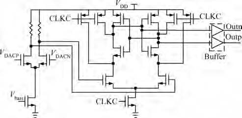
Fig. 1.
Block diagram of the proposed fully differential SAR ADC.
SEMICONDUCTOR INTEGRATED CIRCUITS
Corresponding author: Meng Qiao,Email:mengqiao@seu.edu.cn
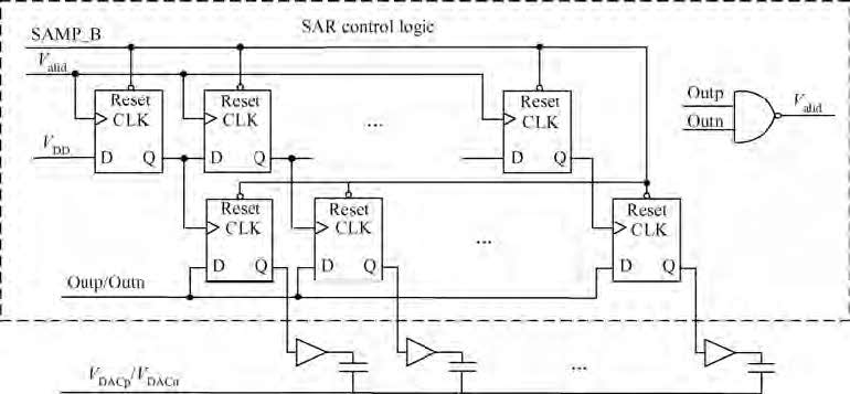
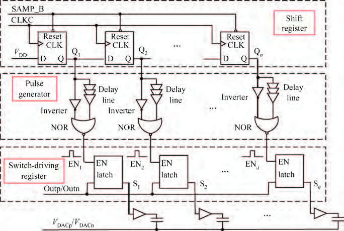
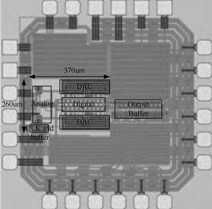
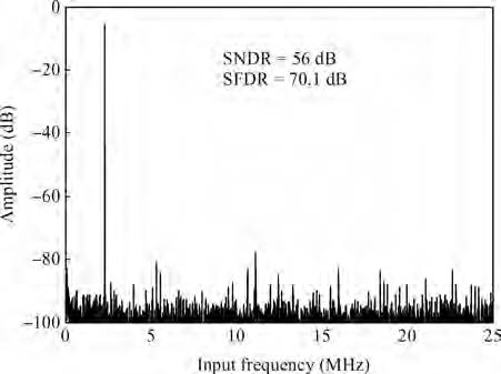
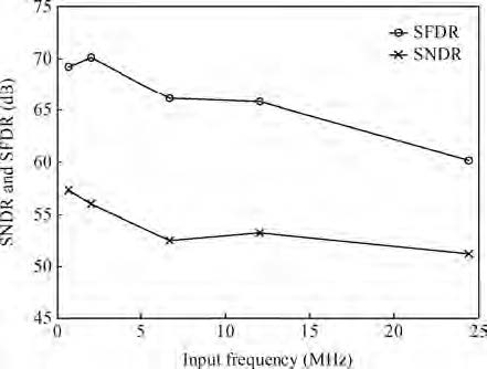
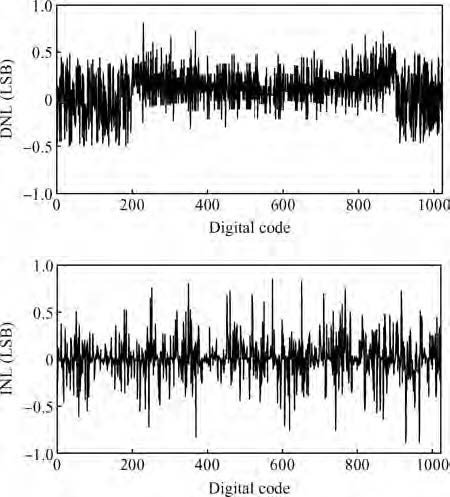
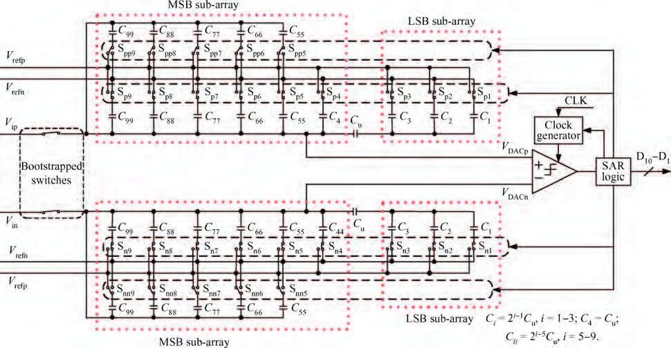
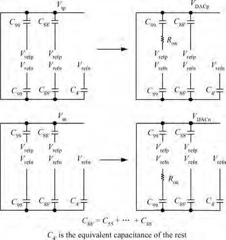
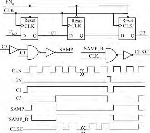
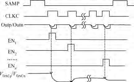
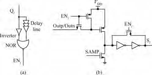
Abstract: This paper presents a 10 bit successive approximation register (SAR) analog-to-digital converter (ADC) in 0.18 μ m 1P6M CMOS technology with a 1.8 V supply voltage. To improve the conversion speed, a partial split capacitor switching scheme is proposed. By reducing the time constant of the bit cycles, the proposed technique shortens the settling time of a capacitive digital-to-analog converter (DAC). In addition, a new SAR control logic is proposed to reduce loop delay to further enhance the conversion speed. At 1.8 V supply voltage and 50 MS/s the SAR ADC achieves a signal-to-noise and distortion ratio (SNDR) of 57.5 dB and spurious-free dynamic range (SFDR) of 69.3 dB. The power consumption is 2.26 mW and the core die area is 0.096 mm2.
Key words: SAR ADC, switching scheme, SAR control logic, DAC, comparator
| [1] | |
| [2] | |
| [3] | |
| [4] | |
| [5] | |
| [6] | |
| [7] | |
| [8] | |
| [9] | |
| [10] | |
| [11] | |
| [12] | |
| [13] | |
| [14] |
| [1] | |
| [2] | |
| [3] | |
| [4] | |
| [5] | |
| [6] | |
| [7] | |
| [8] | |
| [9] | |
| [10] | |
| [11] | |
| [12] | |
| [13] | |
| [14] |


Article views: 5348 Times PDF downloads: 220 Times Cited by: 0 Times
Received: 09 October 2015 Revised: Online: Published: 01 January 2016
| Citation: |
Dong Li, Qiao Meng, Fei Li. A 10 bit 50 MS/s SAR ADC with partial split capacitor switching scheme in 0.18 μm CMOS[J]. Journal of Semiconductors, 2016, 37(1): 015004. doi: 10.1088/1674-4926/37/1/015004
****
D Li, Q Meng, F Li. A 10 bit 50 MS/s SAR ADC with partial split capacitor switching scheme in 0.18 μm CMOS[J]. J. Semicond., 2016, 37(1): 015004. doi: 10.1088/1674-4926/37/1/015004.

|
| [1] | |
| [2] | |
| [3] | |
| [4] | |
| [5] | |
| [6] | |
| [7] | |
| [8] | |
| [9] | |
| [10] | |
| [11] | |
| [12] | |
| [13] | |
| [14] |

 WeChat ID
Journal of Semiconductors © 2017 All Rights Reserved 京ICP备05085259号-2

 DownLoad: