


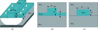
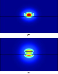
Fig. 1.
(Color online) The structures of silicon nitride: (a) suspended waveguide, (b) rib waveguide, and (c) strip waveguide.
SEMICONDUCTOR DEVICES
Dandan Bian, Xun Lei and Shaowu Chen
Corresponding author: Chen Shaowu,swchen@semi.ac.cn
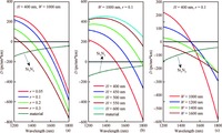
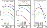
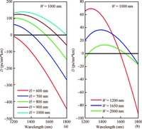
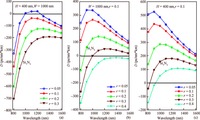
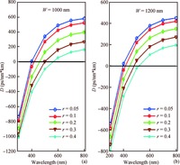
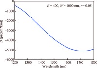
Abstract: We investigate the dispersion properties of nanometer-scaled silicon nitride suspended membrane waveguides around the communication wavelength and systematically study their relationship with the key structural parameters of the waveguide. The simulation results show that a suspended membrane waveguide can realize anomalous dispersion with a relatively thinner silicon nitride thickness in the range of 400 to 600 nm, whereas, for the same membrane thickness, a conventional rib or strip silicon nitride waveguide cannot support anomalous dispersion. In particular, a waveguide with 400 nm silicon nitride thickness and deep etch depth (r=0.05) exhibits anomalous dispersion around the communication wavelength when the waveguide width ranges from 990 to 1255 nm, and the maximum dispersion is 22.56 ps/(nm·km). This specially designed anomalous dispersion silicon nitride waveguide is highly desirable for micro-resonator based optical frequency combs due to its potential to meet the phase-matching condition required for cascaded four-wave-mixing.
Keywords: suspended waveguide, group velocity dispersion, dispersion engineering, frequency comb
| [1] |
Kippenberg T, Spillane S, Vahala K. Kerr-nonlinearity optical parametric oscillation in an ultra high-Q toroid microcavity. Phys Rev Lett, 2004, 93(8):083904 doi: 10.1103/PhysRevLett.93.083904
|
| [2] |
Agha I H, Okawachi Y, Foster M A, et al. Four-wave-mixing parametric oscillations in dispersion-compensated high-Q silica microspheres. Phys Rev A, 2007, 76(4):043837 doi: 10.1103/PhysRevA.76.043837
|
| [3] |
Turner A C, Foster M A, Gaeta A L, et al. Ultra-low power parametric frequency conversion in a silicon microring resonator. Opt Exp, 2008, 16(7):4881 doi: 10.1364/OE.16.004881
|
| [4] |
Bristow A D, Rotenberg N, Van Driel H M. Two-photon absorption and Kerr coefficients of silicon for 850-2200 nm. Appl Phys Lett, 2007, 90(19):191104 doi: 10.1063/1.2737359
|
| [5] |
Liu X, Driscoll J B, Dadap J I, et al. Self-phase modulation and nonlinear loss in silicon nanophotonic wires near the midinfrared two-photon absorption edge. Opt Exp, 2011, 19(8):7778 doi: 10.1364/OE.19.007778
|
| [6] |
Zheng Xuezhi, Luo Ying, Li Guoliang, et al. Enhanced optical bistability from self-heating due to free carrier absorption in substrate removed silicon ring modulators. Opt Exp, 2012, 20(10):11478 doi: 10.1364/OE.20.011478
|
| [7] |
Leuthold J, Koos C, Freude W. Nonlinear silicon photonics. Nat Photonics, 2010, 4(8):535 doi: 10.1038/nphoton.2010.185
|
| [8] |
Okawachi Y, Saha K, Levy J S, et al. Octave-spanning frequency comb generation in a silicon nitride chip. Opt Lett, 2011, 36(17):3398 doi: 10.1364/OL.36.003398
|
| [9] |
Tang Longjuan, Zhang Yinfang, Yang Jinling, et al. Dependence of wet etch rate on deposition, annealing conditions and etchants for PECVD silicon nitride film. Journal of Semiconductors, 2009, 30(9):096005 doi: 10.1088/1674-4926/30/9/096005
|
| [10] |
Chuang W H, Luger T, Fettig R K, et al. Mechanical property characterization of LPCVD silicon nitride thin films at cryogenic temperatures. J Microelectromechan Syst, 2004, 13(5):870 doi: 10.1109/JMEMS.2004.836815
|
| [11] |
Vivien L, Marris-Morini D, Griol A, et al. Vertical multipleslot waveguide ring resonators in silicon nitride. Opt Exp, 2008, 16(22):17237 doi: 10.1364/OE.16.017237
|
| [12] |
Baker C, Stapfner S, Parrain D, et al. Optical instability and selfpulsing in silicon nitride whispering gallery resonators. Opt Exp, 2012, 20(27):29076 doi: 10.1364/OE.20.029076
|
| [13] |
Wang P H, Xuan Y, Fan L, et al. Drop-port study of microresonator frequency combs:power transfer, spectra and timedomain characterization. Opt Exp, 2013, 21(19):22441 doi: 10.1364/OE.21.022441
|
| [14] |
Huang Ying, Luo Xiashu, Song Junfeng, et al. Low loss (< 0.2 dB per transition) CMOS compatible multi-layer Si3N4-on-SOI platform with thermal-optics device integration for silicon photonics. Optical Fiber Communications Conference and Exhibition (OFC), 2014
|
| [15] |
Levy J S, Gondarenko A, Foster M A, et al. CMOS-compatible multiple-wavelength oscillator for on-chip optical interconnects. Nat Photonics, 2010, 4(1):37 doi: 10.1038/nphoton.2009.259
|
| [16] |
Gondarenko A, Levy J S, Lipson M. High confinement micronscale silicon nitride high Q ring resonator. Opt Exp, 2009, 17(14):11366 doi: 10.1364/OE.17.011366
|
| [17] |
Pérez A M, Santiago C, Renero F, et al. Optical properties of amorphous hydrogenated silicon nitride thin films. Opt Eng, 2006, 45(12):123802 doi: 10.1117/1.2402493
|
| [18] |
Malitson I. Interspecimen comparison of the refractive index of fused silica. JOSA 1965, 55(10):1205 doi: 10.1364/JOSA.55.001205
|
| [19] |
Cheng Zhongyuan, Chen Xia, Wong Chiyan, et al. Mid-infrared suspended membrane waveguide and ring resonator on siliconon-insulator. IEEE Photonics J, 2012, 4(5):1510 doi: 10.1109/JPHOT.2012.2210700
|
| [20] |
Zhang Xuezhi, Liu Tiegen, Jiang Junfeng, et al. Mid-infrared frequency comb generation in coupled silicon microring resonators. Opt Commun, 2014, 332:125 doi: 10.1016/j.optcom.2014.06.058
|
| [21] |
Wang Xiaolong, Yan Qingfeng, Liu Jingwei, et al. SOI waveguides fabricated by wet-etching method. Journal of Semiconductors, 2003, 24(10):1026
|


Article views: 3684 Times PDF downloads: 46 Times Cited by: 0 Times
Received: 28 April 2016 Revised: 19 May 2016 Online: Published: 01 November 2016
| Citation: |
Dandan Bian, Xun Lei, Shaowu Chen. Dispersion characteristics of nanometer-scaled silicon nitride suspended membrane waveguides[J]. Journal of Semiconductors, 2016, 37(11): 114007. doi: 10.1088/1674-4926/37/11/114007
****
Dandan Bian and A Bian, X Lei, S W Chen. Dispersion characteristics of nanometer-scaled silicon nitride suspended membrane waveguides[J]. J. Semicond., 2016, 37(11): 114007. doi: 10.1088/1674-4926/37/11/114007.

|
| [1] |
Kippenberg T, Spillane S, Vahala K. Kerr-nonlinearity optical parametric oscillation in an ultra high-Q toroid microcavity. Phys Rev Lett, 2004, 93(8):083904 doi: 10.1103/PhysRevLett.93.083904
|
| [2] |
Agha I H, Okawachi Y, Foster M A, et al. Four-wave-mixing parametric oscillations in dispersion-compensated high-Q silica microspheres. Phys Rev A, 2007, 76(4):043837 doi: 10.1103/PhysRevA.76.043837
|
| [3] |
Turner A C, Foster M A, Gaeta A L, et al. Ultra-low power parametric frequency conversion in a silicon microring resonator. Opt Exp, 2008, 16(7):4881 doi: 10.1364/OE.16.004881
|
| [4] |
Bristow A D, Rotenberg N, Van Driel H M. Two-photon absorption and Kerr coefficients of silicon for 850-2200 nm. Appl Phys Lett, 2007, 90(19):191104 doi: 10.1063/1.2737359
|
| [5] |
Liu X, Driscoll J B, Dadap J I, et al. Self-phase modulation and nonlinear loss in silicon nanophotonic wires near the midinfrared two-photon absorption edge. Opt Exp, 2011, 19(8):7778 doi: 10.1364/OE.19.007778
|
| [6] |
Zheng Xuezhi, Luo Ying, Li Guoliang, et al. Enhanced optical bistability from self-heating due to free carrier absorption in substrate removed silicon ring modulators. Opt Exp, 2012, 20(10):11478 doi: 10.1364/OE.20.011478
|
| [7] |
Leuthold J, Koos C, Freude W. Nonlinear silicon photonics. Nat Photonics, 2010, 4(8):535 doi: 10.1038/nphoton.2010.185
|
| [8] |
Okawachi Y, Saha K, Levy J S, et al. Octave-spanning frequency comb generation in a silicon nitride chip. Opt Lett, 2011, 36(17):3398 doi: 10.1364/OL.36.003398
|
| [9] |
Tang Longjuan, Zhang Yinfang, Yang Jinling, et al. Dependence of wet etch rate on deposition, annealing conditions and etchants for PECVD silicon nitride film. Journal of Semiconductors, 2009, 30(9):096005 doi: 10.1088/1674-4926/30/9/096005
|
| [10] |
Chuang W H, Luger T, Fettig R K, et al. Mechanical property characterization of LPCVD silicon nitride thin films at cryogenic temperatures. J Microelectromechan Syst, 2004, 13(5):870 doi: 10.1109/JMEMS.2004.836815
|
| [11] |
Vivien L, Marris-Morini D, Griol A, et al. Vertical multipleslot waveguide ring resonators in silicon nitride. Opt Exp, 2008, 16(22):17237 doi: 10.1364/OE.16.017237
|
| [12] |
Baker C, Stapfner S, Parrain D, et al. Optical instability and selfpulsing in silicon nitride whispering gallery resonators. Opt Exp, 2012, 20(27):29076 doi: 10.1364/OE.20.029076
|
| [13] |
Wang P H, Xuan Y, Fan L, et al. Drop-port study of microresonator frequency combs:power transfer, spectra and timedomain characterization. Opt Exp, 2013, 21(19):22441 doi: 10.1364/OE.21.022441
|
| [14] |
Huang Ying, Luo Xiashu, Song Junfeng, et al. Low loss (< 0.2 dB per transition) CMOS compatible multi-layer Si3N4-on-SOI platform with thermal-optics device integration for silicon photonics. Optical Fiber Communications Conference and Exhibition (OFC), 2014
|
| [15] |
Levy J S, Gondarenko A, Foster M A, et al. CMOS-compatible multiple-wavelength oscillator for on-chip optical interconnects. Nat Photonics, 2010, 4(1):37 doi: 10.1038/nphoton.2009.259
|
| [16] |
Gondarenko A, Levy J S, Lipson M. High confinement micronscale silicon nitride high Q ring resonator. Opt Exp, 2009, 17(14):11366 doi: 10.1364/OE.17.011366
|
| [17] |
Pérez A M, Santiago C, Renero F, et al. Optical properties of amorphous hydrogenated silicon nitride thin films. Opt Eng, 2006, 45(12):123802 doi: 10.1117/1.2402493
|
| [18] |
Malitson I. Interspecimen comparison of the refractive index of fused silica. JOSA 1965, 55(10):1205 doi: 10.1364/JOSA.55.001205
|
| [19] |
Cheng Zhongyuan, Chen Xia, Wong Chiyan, et al. Mid-infrared suspended membrane waveguide and ring resonator on siliconon-insulator. IEEE Photonics J, 2012, 4(5):1510 doi: 10.1109/JPHOT.2012.2210700
|
| [20] |
Zhang Xuezhi, Liu Tiegen, Jiang Junfeng, et al. Mid-infrared frequency comb generation in coupled silicon microring resonators. Opt Commun, 2014, 332:125 doi: 10.1016/j.optcom.2014.06.058
|
| [21] |
Wang Xiaolong, Yan Qingfeng, Liu Jingwei, et al. SOI waveguides fabricated by wet-etching method. Journal of Semiconductors, 2003, 24(10):1026
|

 WeChat ID
Journal of Semiconductors © 2017 All Rights Reserved 京ICP备05085259号-2

 DownLoad:

