J. Semicond. > 2016, Volume 37 > Issue 11 > 115001

SEMICONDUCTOR INTEGRATED CIRCUITS

Non-equilibrium carrier capture, recombination and annealing in thick insulators and their impact on radiation hardness

G.I. Zebrev, M.G. Drosdetsky and A.M. Galimov

+ Author Affiliations

 Corresponding author: G. I. Zebrev,gizebrev@mephi.ru

DOI: 10.1088/1674-4926/37/11/115001

PDF

Abstract: This paper describes an approach to prediction of the thick insulators' radiation response based on modeling of the charge yield, which is dependent on irradiation temperature, dose rate, and electric field magnitudes. Temperature behavior of the charge yield and degradation saturation due to the interface precursor depletion has been modeled and simulated. Competition between the time-dependent and true dose rate (ELDRS) effects has been simulated and discussed within a framework of the rate-equation-based mathematical model. It was shown that the precursor trap in the thick insulating oxides can be important at high dose rates. It was also shown that full filling of the shallow hole traps in the insulating oxide bulk can cause suppression of dose-rate sensitivity at relatively high dose rates, especially in thick insulators.

Key words: bipolar devicestotal dose effectsdose rate effectsELDRSinsulatorsmodeling


[1]
Fleetwood D M. Total ionizing dose effects in MOS and lowdose-rate-sensitive linear-bipolar devices. IEEE Trans Nucl Sci, 2013, 60(3):1706 doi: 10.1109/TNS.2013.2259260
[2]
Oldham T R. Basic mechanisms of TID and DDD response in MOS and bipolar microelectronics. NSREC Short Course, 2011
[3]
Schwank J R. Total-dose effects in MOS devices. NSREC Short Course, 2002
[4]
Hjalmarson H P, Pease R L, Witczak S C, et al. Mechanisms for radiation dose-rate sensitivity of bipolar transistors. IEEE Trans Nucl Sci, 2003, 50:1901 doi: 10.1109/TNS.2003.821803
[5]
Zebrev G I, Pavlov D Y, Pershenkov V S, et al. Radiation response of bipolar transistors at various irradiation temperatures and electric biases. IEEE Trans Nucl Sci, 2006, 53(4):1981 doi: 10.1109/TNS.2006.877851
[6]
Zebrev G I. Modeling and simulation of the enhanced low-doserate sensitivity of thick isolating layers in advanced ICs. Russian Microelectronics, 2006, 35(3):177 doi: 10.1134/S1063739706030061
[7]
Zebrev G I, Gorbunov M S. Modeling of radiation-induced leakage and low dose-rate effects in thick edge isolation of modern MOSFETs. IEEE Trans Nucl Sci, 2009, 56(4):2230 doi: 10.1109/TNS.2009.2016096
[8]
[9]
Johnston A H, Swimm R T, Thorbourn D O. Total dose effects on bipolar integrated circuits at low temperature. IEEE Trans Nucl Sci, 2012, 59(6):2995 doi: 10.1109/TNS.2012.2219592
[10]
Johnston A H, Swimm R T, Thorbourn D O. Charge yield at low electric fields:considerations for bipolar integrated circuits. IEEE Trans Nucl Sci, 2013, 60(6):4488 doi: 10.1109/TNS.2013.2283515
[11]
Johnston A H, Swimm R T, Thorbourn D O, et al. Field dependence of charge yield in silicon dioxide:considerations for bipolar integrated circuits. IEEE Trans Nucl Sci, 2014, 61(6):2818 doi: 10.1109/TNS.2014.2367512
[12]
Hughes R C. Carrier-carrier transport phenomena in amorphous SiO2:direct measurement of the drift mobility and lifetime. Phys Rev Lett, 1973, 30(26):1333 doi: 10.1103/PhysRevLett.30.1333
[13]
McLean F B, Boesch H E Jr, McGarrity J M. Hole transport and recovery characteristics of gate insulators. IEEE Trans Nucl Sci, 1976, 23(6):1506 doi: 10.1109/TNS.1976.4328530
[14]
Adell P C, Esqueda I S, Barnaby H J, et al. Impact of low temperatures on the total ionizing dose response and ELDRS in gated lateral PNP BJTs. IEEE Trans Nucl Sci, 2012, 59(6):3081 doi: 10.1109/TNS.2012.2224372
[15]
Saks N S, Klein R B, Griscom D L. Formation of interface traps in MOSFETS during annealing following low temperature irradiation. IEEE Trans Nucl Sci, 1987, 35(6):1234 http://cn.bing.com/academic/profile?id=2015312387&encoded=0&v=paper_preview&mkt=zh-cn
[16]
Boesch H E, McLean F B. Hole transport and trapping in field oxides. IEEE Trans Nucl Sci, 1985, 32(6):3940 doi: 10.1109/TNS.1985.4334047
[17]
McLean F B, Ausman G A Jr, Boesch H E Jr, et al. Application of stochastic hopping transport to hole conduction in amorphous SiO2. J Appl Phys, 1976, 47:1529 doi: 10.1063/1.322767
[18]
Scher H, Montroll E W. Anomalous transit-time dispersion in amorphous solids. Phys Rev B, 1975, 12(6):2455 http://cn.bing.com/academic/profile?id=1967200406&encoded=0&v=paper_preview&mkt=zh-cn
[19]
Drosdetsky M G, Zebrev G I, Galimov A M, et al. Physical mechanisms of radiation response in thick isolation oxides for different temperatures and dose rates. Proceedings of 15th European Conference on Radiation and Its Effects on Components and Systems (RADECS), 2015:1 http://cn.bing.com/academic/profile?id=2314788901&encoded=0&v=paper_preview&mkt=zh-cn
[20]
Ma T P, Dressendorfer P V. Radiation effects in MOS devices and integrated circuits. New-York:John Wiley & Sons, 1988
[21]
Woods M, Williams R. Hole traps in silicon dioxide. J Appl Phys, 1976, 47(3):1082 doi: 10.1063/1.322730
[22]
Boch J, Saigne F, Ducret S, et al. Total dose effects on bipolar integrated circuits:characterization of the saturation region. IEEE Trans Nucl Sci, 2004, 51(6):3225 doi: 10.1109/TNS.2004.839143
[23]
Zebrev G I, Drosdetsky M G, Galimov A M, et al. Modeling and simulation of dose effects in bipolar analog integrated circuits. International Conference on Micro-and Nano-Electronics, 2014:94401C http://cn.bing.com/academic/profile?id=2053438435&encoded=0&v=paper_preview&mkt=zh-cn
[24]
Zebrev G I, Petrov A S, Useinov R G, et al. Simulation of bipolar transistor degradation at various dose rates and electric modes for high dose conditions. IEEE Trans Nucl Sci, 2014, 61(4):1785 doi: 10.1109/TNS.2014.2315672
[25]
Zhao Qifeng, Zhuang Yiqi, Bao Junlin, et al. Model of radiationinduced gain degradation of NPN bipolar junction transistor at different dose rates. Journal of Semiconductors, 2015, 36(6):064007 doi: 10.1088/1674-4926/36/6/064007
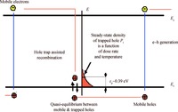
Fig. 1.  (Color online) Mechanism of electron-hole recombination through the localized hole levels near the valence band edge of the silicon oxide.

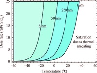
Fig. 2.  (Color online) Irradiation temperature-dose rate domain showing the separation lines between the regions with different saturation types, calculated with Equation (7) for 4 oxide thicknesses, ∑p= 2 × 10-15 cm2, εa = 0.7 eV, τa0 = 10-7 s.

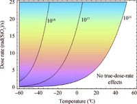
Fig. 3.  (Color online) Irradiation temperature-dose rate domain showing the demarcation lines between the regions with presence and absence of true dose-rate effects, calculated with Equation (7) for Ntp=1016, 1017, 1018 cm-3, dox = 0.8 μm, εp =0.39 eV, Eox =5 ×10⁴ V/cm, ηG =0.5.

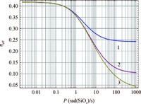
Fig. 4.  (Color online) Effective charge yield as functions of dose rate calculated for oxides with different densities of the hole traps (1) Ntp = 1016 cm-3; (2) Ntp = 1017 cm-3; (3) Ntp = 1018 cm-3.

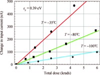
Fig. 5.  (Color online) Increase in input bias current versus dose for irradiations with P= 0.005 rad (SiO2)/s at different low temperatures. Fitted parameters: Eox}=2.5 ×10⁵ V/cm, IC}=5.1 mA, Frd=1.65× 10⁻³, εp=0.39 eV, Ntp= 7 × 1017 cm-3 (see Appendix).

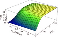
Fig. 6.  (Color online) Effective charge yield as function of the oxide electric field and irradiation temperature calculated for εp=0.39 eV, dox=0.8 μm.

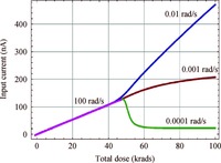
Fig. 7.  (Color online) Simulated dose rate switching curves: switching to different lower dose rates Frd}=1.45×10⁻², τa =3 ×10⁷ s, dox=1 μm, T=27 ℃. Notice that quantitative view of the radiation response may vary depending on chosen parameters. No ELDRS effects are observed at high electric fields and for thin oxides.

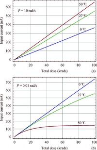
Fig. 8.  (Color online) Dose dependencies of the base current simulated at the dose rates P=10 rad/s (a) and P=0.01 rad/s (b) with the different irradiation temperatures T=0, 27, and 50 ℃. Simulation parameters: Frd=1.45 × 10⁻², τaa0\exp(εa/kT), τa0=2× 10⁻⁶ s, εa= 0.743 eV, dox=1 μm, IC=87 μA, Eox=1.5× 10⁵ V/cm.

[1]
Fleetwood D M. Total ionizing dose effects in MOS and lowdose-rate-sensitive linear-bipolar devices. IEEE Trans Nucl Sci, 2013, 60(3):1706 doi: 10.1109/TNS.2013.2259260
[2]
Oldham T R. Basic mechanisms of TID and DDD response in MOS and bipolar microelectronics. NSREC Short Course, 2011
[3]
Schwank J R. Total-dose effects in MOS devices. NSREC Short Course, 2002
[4]
Hjalmarson H P, Pease R L, Witczak S C, et al. Mechanisms for radiation dose-rate sensitivity of bipolar transistors. IEEE Trans Nucl Sci, 2003, 50:1901 doi: 10.1109/TNS.2003.821803
[5]
Zebrev G I, Pavlov D Y, Pershenkov V S, et al. Radiation response of bipolar transistors at various irradiation temperatures and electric biases. IEEE Trans Nucl Sci, 2006, 53(4):1981 doi: 10.1109/TNS.2006.877851
[6]
Zebrev G I. Modeling and simulation of the enhanced low-doserate sensitivity of thick isolating layers in advanced ICs. Russian Microelectronics, 2006, 35(3):177 doi: 10.1134/S1063739706030061
[7]
Zebrev G I, Gorbunov M S. Modeling of radiation-induced leakage and low dose-rate effects in thick edge isolation of modern MOSFETs. IEEE Trans Nucl Sci, 2009, 56(4):2230 doi: 10.1109/TNS.2009.2016096
[8]
[9]
Johnston A H, Swimm R T, Thorbourn D O. Total dose effects on bipolar integrated circuits at low temperature. IEEE Trans Nucl Sci, 2012, 59(6):2995 doi: 10.1109/TNS.2012.2219592
[10]
Johnston A H, Swimm R T, Thorbourn D O. Charge yield at low electric fields:considerations for bipolar integrated circuits. IEEE Trans Nucl Sci, 2013, 60(6):4488 doi: 10.1109/TNS.2013.2283515
[11]
Johnston A H, Swimm R T, Thorbourn D O, et al. Field dependence of charge yield in silicon dioxide:considerations for bipolar integrated circuits. IEEE Trans Nucl Sci, 2014, 61(6):2818 doi: 10.1109/TNS.2014.2367512
[12]
Hughes R C. Carrier-carrier transport phenomena in amorphous SiO2:direct measurement of the drift mobility and lifetime. Phys Rev Lett, 1973, 30(26):1333 doi: 10.1103/PhysRevLett.30.1333
[13]
McLean F B, Boesch H E Jr, McGarrity J M. Hole transport and recovery characteristics of gate insulators. IEEE Trans Nucl Sci, 1976, 23(6):1506 doi: 10.1109/TNS.1976.4328530
[14]
Adell P C, Esqueda I S, Barnaby H J, et al. Impact of low temperatures on the total ionizing dose response and ELDRS in gated lateral PNP BJTs. IEEE Trans Nucl Sci, 2012, 59(6):3081 doi: 10.1109/TNS.2012.2224372
[15]
Saks N S, Klein R B, Griscom D L. Formation of interface traps in MOSFETS during annealing following low temperature irradiation. IEEE Trans Nucl Sci, 1987, 35(6):1234 http://cn.bing.com/academic/profile?id=2015312387&encoded=0&v=paper_preview&mkt=zh-cn
[16]
Boesch H E, McLean F B. Hole transport and trapping in field oxides. IEEE Trans Nucl Sci, 1985, 32(6):3940 doi: 10.1109/TNS.1985.4334047
[17]
McLean F B, Ausman G A Jr, Boesch H E Jr, et al. Application of stochastic hopping transport to hole conduction in amorphous SiO2. J Appl Phys, 1976, 47:1529 doi: 10.1063/1.322767
[18]
Scher H, Montroll E W. Anomalous transit-time dispersion in amorphous solids. Phys Rev B, 1975, 12(6):2455 http://cn.bing.com/academic/profile?id=1967200406&encoded=0&v=paper_preview&mkt=zh-cn
[19]
Drosdetsky M G, Zebrev G I, Galimov A M, et al. Physical mechanisms of radiation response in thick isolation oxides for different temperatures and dose rates. Proceedings of 15th European Conference on Radiation and Its Effects on Components and Systems (RADECS), 2015:1 http://cn.bing.com/academic/profile?id=2314788901&encoded=0&v=paper_preview&mkt=zh-cn
[20]
Ma T P, Dressendorfer P V. Radiation effects in MOS devices and integrated circuits. New-York:John Wiley & Sons, 1988
[21]
Woods M, Williams R. Hole traps in silicon dioxide. J Appl Phys, 1976, 47(3):1082 doi: 10.1063/1.322730
[22]
Boch J, Saigne F, Ducret S, et al. Total dose effects on bipolar integrated circuits:characterization of the saturation region. IEEE Trans Nucl Sci, 2004, 51(6):3225 doi: 10.1109/TNS.2004.839143
[23]
Zebrev G I, Drosdetsky M G, Galimov A M, et al. Modeling and simulation of dose effects in bipolar analog integrated circuits. International Conference on Micro-and Nano-Electronics, 2014:94401C http://cn.bing.com/academic/profile?id=2053438435&encoded=0&v=paper_preview&mkt=zh-cn
[24]
Zebrev G I, Petrov A S, Useinov R G, et al. Simulation of bipolar transistor degradation at various dose rates and electric modes for high dose conditions. IEEE Trans Nucl Sci, 2014, 61(4):1785 doi: 10.1109/TNS.2014.2315672
[25]
Zhao Qifeng, Zhuang Yiqi, Bao Junlin, et al. Model of radiationinduced gain degradation of NPN bipolar junction transistor at different dose rates. Journal of Semiconductors, 2015, 36(6):064007 doi: 10.1088/1674-4926/36/6/064007
  • Search

    Advanced Search >>

    GET CITATION

    shu

    Export: BibTex EndNote

    Article Metrics

    Article views: 3159 Times PDF downloads: 24 Times Cited by: 0 Times

    History

    Received: 22 February 2016 Revised: 17 May 2016 Online: Published: 01 November 2016

    Catalog

      Email This Article

      User name:
      Email:*请输入正确邮箱
      Code:*验证码错误
      G.I. Zebrev, M.G. Drosdetsky, A.M. Galimov. Non-equilibrium carrier capture, recombination and annealing in thick insulators and their impact on radiation hardness[J]. Journal of Semiconductors, 2016, 37(11): 115001. doi: 10.1088/1674-4926/37/11/115001 ****G.I. Zebrev, M.G. Drosdetsky, A.M. Galimov. Non-equilibrium carrier capture, recombination and annealing in thick insulators and their impact on radiation hardness[J]. J. Semicond., 2016, 37(11): 115001. doi: 10.1088/1674-4926/37/11/115001.
      Citation:
      G.I. Zebrev, M.G. Drosdetsky, A.M. Galimov. Non-equilibrium carrier capture, recombination and annealing in thick insulators and their impact on radiation hardness[J]. Journal of Semiconductors, 2016, 37(11): 115001. doi: 10.1088/1674-4926/37/11/115001 ****
      G.I. Zebrev, M.G. Drosdetsky, A.M. Galimov. Non-equilibrium carrier capture, recombination and annealing in thick insulators and their impact on radiation hardness[J]. J. Semicond., 2016, 37(11): 115001. doi: 10.1088/1674-4926/37/11/115001.

      Non-equilibrium carrier capture, recombination and annealing in thick insulators and their impact on radiation hardness

      DOI: 10.1088/1674-4926/37/11/115001
      More Information
      • Corresponding author: G. I. Zebrev,gizebrev@mephi.ru
      • Received Date: 2016-02-22
      • Revised Date: 2016-05-17
      • Published Date: 2016-11-01

      Catalog

        /

        DownLoad:  Full-Size Img  PowerPoint
        Return
        Return