


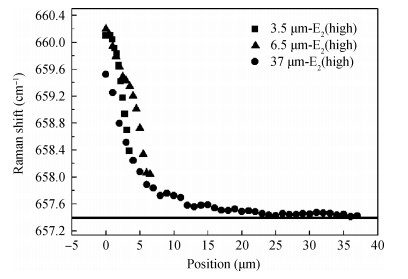
Fig. 1.
The position-dependent E2 (high) peak values of Raman spectra. The solid line shows the stress-free frequency of 657.4 cm-1 [17].
SEMICONDUCTOR MATERIALS
Maosong Sun1, 2, Jicai Zhang2, 3, , Jun Huang2, Xuewei Li2, Linjun Wang1, Xuehua Liu2, Jianfeng Wang2, 3 and Ke Xu2, 3,
Corresponding author: Zhang Jicai, Email:jczhang2010@sinano.ac.cn; Xu Ke, Email:kxu2006@sinano.ac.cn
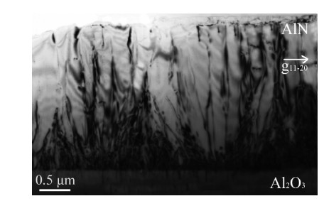
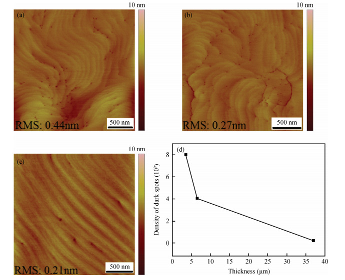
Abstract: AlN thick films were grown on c-plane sapphire substrates by hydride vapor phase epitaxy at high temperature. The evolution of the strain state and crystal quality of AlN with increase of thickness were investigated by transmission electron microscopy, field-emission scanning electron microscopy, Raman spectra and atomic force microscopy (AFM). As the thickness increased, the stress in the epilayers decreased gradually, which was attributed to the reaction of dislocations at the first several microns in thickness. When the thickness was more than 20 μm, the stress was almost fully relaxed due to the formation of cracks. Wet etching experiments indicated that the dislocation density decreased with the increase of thickness. The AFM images showed that the density of dark spots on the surface obviously decreased and the atomic steps became straight as the thickness increased.
Keywords: AlN, HVPE, surface morphology, strain state
| [1] |
Oto T, Banal R G, Kataoka K, et al. 100 mW deep-ultraviolet emission from aluminum-nitride-based quantum wells pumped by an electron beam. Nat Photonics, 2010, 4: 767 doi: 10.1038/nphoton.2010.220
|
| [2] |
Zhang J C, Zhu Y H, Egawa T, et al. Suppression of the subband parasitic peak by 1 nm i-AlN interlayer in AlGaN deep ultraviolet light-emitting diodes. Appl Phys Lett, 2008, 93: 131117 doi: 10.1063/1.2996580
|
| [3] |
Yang Min, Chong Ming, Zhao Degang, et al. Back-illuminated AlxGa1-xN-based dual-band solar-blind ultraviolet photodetectors. Journal of Semiconductors, 2014, 35(6): 064008 doi: 10.1088/1674-4926/35/6/064008
|
| [4] |
Li Wei, Jin Peng, Wang Weiying, et al. Anomalous temperature-dependent photoluminescence peak energy in InAlN alloys. Journal of Semiconductors, 2014, 35(9): 093001 doi: 10.1088/1674-4926/35/9/093001
|
| [5] |
Li Bin, Wei Lan, Wen Cai. Static characteristics and short channel effect in enhancement-mode AlN/GaN/AlN N-polar MISFET with self-aligned source/drain regions. Journal of Semiconductors, 2014, 35(12): 124006 doi: 10.1088/1674-4926/35/12/124006
|
| [6] |
Sun M S, Zhang J C, Huang J, et al. AlN thin film grown on different substrates by hydride vapor phase epitaxy. J Cryst Growth, 2016, 436: 62 doi: 10.1016/j.jcrysgro.2015.11.040
|
| [7] |
Chen Y R, Song H, Li D B, et al. Influence of the growth temperature of AlN nucleation layer on AlN template grown by high-temperature MOCVD. Mater Lett, 2014, 114: 26 doi: 10.1016/j.matlet.2013.09.096
|
| [8] |
Banal R G, Funato M, Kawakami Y. Initial nucleation of AlN grown directly on sapphire substrates by metal-organic vapor phase epitaxy. Appl Phys Lett, 2008, 92: 241905 doi: 10.1063/1.2937445
|
| [9] |
Jain R, Sun W, Yang J, et al. Migration enhanced lateral epitaxial overgrowth of AlN and AlGaN for high reliability deep ultraviolet light emitting diodes. Appl Phys Lett 2008, 93: 051113 doi: 10.1063/1.2969402
|
| [10] |
Takeuchi M, Ooishi S, Ohtsuka T, et al. Improvement of Al-polar AlN layer quality by three-stage flow-modulation metalorganic chemical vapor deposition. Appl Phys Express, 2008, 1: 021102 doi: 10.1143/APEX.1.021102
|
| [11] |
Hirayama H, Yatabe T, Noguchi N, et al. 23-261 nm AlGaN deep-ultraviolet light-emitting diodes fabricated on AlN multilayer buffers grown by ammonia pulse-flow method on sapphire. Appl Phys Lett, 2007, 91: 071901 doi: 10.1063/1.2770662
|
| [12] |
Balakrishnan K, Bandohi A, Iwaya M, et al. Influence of high temperature in the growth of low dislocation content AlN bridge layers on patterned 6H-SiC substrates by metalorganic vapor phase epitaxy. Jpn J Appl Phys, 2007, 46: L307 doi: 10.1143/JJAP.46.L307
|
| [13] |
Okada N, Kato N, Sato S, et al. Epitaxial lateral overgrowth of a-AlN layer on patterned a-AlN template by HT-MOVPE. J Cryst Growth, 2007, 300: 141 doi: 10.1016/j.jcrysgro.2006.11.025
|
| [14] |
Pons M, Boichot R, Coudurier N, et al. High temperature chemical vapor deposition of aluminum nitride, growth and evaluation. Surface & Coatings Technology, 2013, 230: 111
|
| [15] |
Sun X J, Li D B, Chen Y, et al. In situ observation of two-step growth of AlN on sapphire using high-temperature metal-organic chemical vapour deposition. Cryst Eng Comm, 2013, 15: 6066 doi: 10.1039/c3ce40755a
|
| [16] |
Hirayama H, Fujikawa S, Kamata N. Recent progress in AlGaN-based deep-UV LEDs. Electron Commun Jpn, 2015, 98(5): 1 doi: 10.1002/ecj.2015.98.issue-5
|
| [17] |
Prokofyeva T, Seon M, Vanbuskirk J, et al. Vibrational properties of AlN grown on (111)-oriented silicon. Phys Rev B, 2001(63): 125313
|
| [18] |
Yang S, Miyagawa R, Miyake H, et al. Raman scattering spectroscopy of residual stresses in epitaxial AlN films. Appl Phys Express, 2011(43): 031001
|
| [19] |
Zhao Danmei, Zhao Degang, Jiang Desheng, et al. Impact of GaN transition layers in the growth of GaN epitaxial layer on silicon. Journal of Semiconductors, 2015, 36(6): 063003 doi: 10.1088/1674-4926/36/6/063003
|
| [20] |
Kim I H, Park H S, Park Y J. Formation of V-shaped pits in InGaN/GaN multiquantum wells and bulk InGaN films. Appl Phys Lett, 1998, 73: 1634 doi: 10.1063/1.122229
|


Article views: 3970 Times PDF downloads: 45 Times Cited by: 0 Times
Received: 20 May 2016 Revised: 06 June 2016 Online: Published: 01 December 2016
| Citation: |
Maosong Sun, Jicai Zhang, Jun Huang, Xuewei Li, Linjun Wang, Xuehua Liu, Jianfeng Wang, Ke Xu. Influence of thickness on strain state and surface morphology of AlN grown by HVPE[J]. Journal of Semiconductors, 2016, 37(12): 123001. doi: 10.1088/1674-4926/37/12/123001
****
M S Sun, J C Zhang, J Huang, X W Li, L J Wang, X H Liu, J F Wang, K Xu. Influence of thickness on strain state and surface morphology of AlN grown by HVPE[J]. J. Semicond., 2016, 37(12): 123001. doi: 10.1088/1674-4926/37/12/123001.

|
| [1] |
Oto T, Banal R G, Kataoka K, et al. 100 mW deep-ultraviolet emission from aluminum-nitride-based quantum wells pumped by an electron beam. Nat Photonics, 2010, 4: 767 doi: 10.1038/nphoton.2010.220
|
| [2] |
Zhang J C, Zhu Y H, Egawa T, et al. Suppression of the subband parasitic peak by 1 nm i-AlN interlayer in AlGaN deep ultraviolet light-emitting diodes. Appl Phys Lett, 2008, 93: 131117 doi: 10.1063/1.2996580
|
| [3] |
Yang Min, Chong Ming, Zhao Degang, et al. Back-illuminated AlxGa1-xN-based dual-band solar-blind ultraviolet photodetectors. Journal of Semiconductors, 2014, 35(6): 064008 doi: 10.1088/1674-4926/35/6/064008
|
| [4] |
Li Wei, Jin Peng, Wang Weiying, et al. Anomalous temperature-dependent photoluminescence peak energy in InAlN alloys. Journal of Semiconductors, 2014, 35(9): 093001 doi: 10.1088/1674-4926/35/9/093001
|
| [5] |
Li Bin, Wei Lan, Wen Cai. Static characteristics and short channel effect in enhancement-mode AlN/GaN/AlN N-polar MISFET with self-aligned source/drain regions. Journal of Semiconductors, 2014, 35(12): 124006 doi: 10.1088/1674-4926/35/12/124006
|
| [6] |
Sun M S, Zhang J C, Huang J, et al. AlN thin film grown on different substrates by hydride vapor phase epitaxy. J Cryst Growth, 2016, 436: 62 doi: 10.1016/j.jcrysgro.2015.11.040
|
| [7] |
Chen Y R, Song H, Li D B, et al. Influence of the growth temperature of AlN nucleation layer on AlN template grown by high-temperature MOCVD. Mater Lett, 2014, 114: 26 doi: 10.1016/j.matlet.2013.09.096
|
| [8] |
Banal R G, Funato M, Kawakami Y. Initial nucleation of AlN grown directly on sapphire substrates by metal-organic vapor phase epitaxy. Appl Phys Lett, 2008, 92: 241905 doi: 10.1063/1.2937445
|
| [9] |
Jain R, Sun W, Yang J, et al. Migration enhanced lateral epitaxial overgrowth of AlN and AlGaN for high reliability deep ultraviolet light emitting diodes. Appl Phys Lett 2008, 93: 051113 doi: 10.1063/1.2969402
|
| [10] |
Takeuchi M, Ooishi S, Ohtsuka T, et al. Improvement of Al-polar AlN layer quality by three-stage flow-modulation metalorganic chemical vapor deposition. Appl Phys Express, 2008, 1: 021102 doi: 10.1143/APEX.1.021102
|
| [11] |
Hirayama H, Yatabe T, Noguchi N, et al. 23-261 nm AlGaN deep-ultraviolet light-emitting diodes fabricated on AlN multilayer buffers grown by ammonia pulse-flow method on sapphire. Appl Phys Lett, 2007, 91: 071901 doi: 10.1063/1.2770662
|
| [12] |
Balakrishnan K, Bandohi A, Iwaya M, et al. Influence of high temperature in the growth of low dislocation content AlN bridge layers on patterned 6H-SiC substrates by metalorganic vapor phase epitaxy. Jpn J Appl Phys, 2007, 46: L307 doi: 10.1143/JJAP.46.L307
|
| [13] |
Okada N, Kato N, Sato S, et al. Epitaxial lateral overgrowth of a-AlN layer on patterned a-AlN template by HT-MOVPE. J Cryst Growth, 2007, 300: 141 doi: 10.1016/j.jcrysgro.2006.11.025
|
| [14] |
Pons M, Boichot R, Coudurier N, et al. High temperature chemical vapor deposition of aluminum nitride, growth and evaluation. Surface & Coatings Technology, 2013, 230: 111
|
| [15] |
Sun X J, Li D B, Chen Y, et al. In situ observation of two-step growth of AlN on sapphire using high-temperature metal-organic chemical vapour deposition. Cryst Eng Comm, 2013, 15: 6066 doi: 10.1039/c3ce40755a
|
| [16] |
Hirayama H, Fujikawa S, Kamata N. Recent progress in AlGaN-based deep-UV LEDs. Electron Commun Jpn, 2015, 98(5): 1 doi: 10.1002/ecj.2015.98.issue-5
|
| [17] |
Prokofyeva T, Seon M, Vanbuskirk J, et al. Vibrational properties of AlN grown on (111)-oriented silicon. Phys Rev B, 2001(63): 125313
|
| [18] |
Yang S, Miyagawa R, Miyake H, et al. Raman scattering spectroscopy of residual stresses in epitaxial AlN films. Appl Phys Express, 2011(43): 031001
|
| [19] |
Zhao Danmei, Zhao Degang, Jiang Desheng, et al. Impact of GaN transition layers in the growth of GaN epitaxial layer on silicon. Journal of Semiconductors, 2015, 36(6): 063003 doi: 10.1088/1674-4926/36/6/063003
|
| [20] |
Kim I H, Park H S, Park Y J. Formation of V-shaped pits in InGaN/GaN multiquantum wells and bulk InGaN films. Appl Phys Lett, 1998, 73: 1634 doi: 10.1063/1.122229
|

 WeChat ID
Journal of Semiconductors © 2017 All Rights Reserved 京ICP备05085259号-2

 DownLoad:

