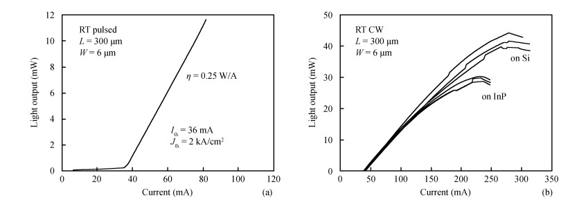
| [1] |
Fang A W, Park H, Cohen O, et al. Electrically pumped hybrid AlGaInAs-silicon evanescent laser. Optics Express, 2006, 14(20): 9203 doi: 10.1364/OE.14.009203 |
| [2] |
|
| [3] |
Liang Di, Roelkens G, Baets R, et al. Hybrid integrated platforms for silicon photonics. Materials, 2010, 3(3):1782 doi: 10.3390/ma3031782 |
| [4] |
Chen Hongda. Microelectronic and optoelectronic integrated technology. Beijing: Publishing House of Electronics Industry, 2008
|
| [5] |
Zhao Hongquan. Research of Si and InP bonding and the development of Si based InGaAsP laser. Doctoral Dissertation, Institute of Semiconductors, Chinese Academy of Sciences, 2006
|
| [6] |
Wang Xiaoqing, Yu Yude, Ning Jin. Researching the silicon direct wafer bonding with interfacial SiO 2 layer. Journal of Semiconductors, 2016, 37(5): 056001 doi: 10.1088/1674-4926/37/5/056001 |
| [7] |
|
| [8] |
Taylor G W, Evaldsson P A. Temperature dependent operation of the vertical cavity surface emitting laser. IEEE J Quantum Electron, 1994, 30(10): 2262 doi: 10.1109/3.328601 |
| [9] |
Esser R H, Hobart K D, Kub F J. Directional diffusion and void formation at a Si (001) bonded wafer interface. J Appl Phys, 2002, 92(4): 1945 doi: 10.1063/1.1491590 |
| [10] |
Tong Q Y, Goesele U. Semiconductor wafer bonding: science and technology. John Wiley, 1999
|
| [11] |
Wada H, Kamijoh T. 1.3 μm InP-InGaAsP lasers fabricated on Si substrates by wafer bonding. IEEE J Sel Topics Quantum Electron, 1997, 3(3): 937 doi: 10.1109/2944.640647 |
| [12] |
Tanabe K, Watanabe K, Arakawa Y. 1.3 μm InAs/GaAs quantum dot lasers on Si rib structures with current injection across direct-bonded GaAs/Si heterointerfaces. Optics Express, 2012, 20(26): B315 doi: 10.1364/OE.20.00B315 |
| [13] |
Tanabe K, Watanabe K, Arakawa Y. Ⅲ-Ⅴ/Si hybrid photonic devices by direct fusion bonding. Scientific Reports, 2012, 2: 349
|
| [14] |
Eaton W P, Risbud S H, Smith R L. Silicon wafer-to-wafer bonding at T < 200℃ with polymethylmethacrylate. Appl Phys Lett, 1994, 65(4): 439 doi: 10.1063/1.112326 |
| [15] |
|
| [16] |
Zhao Huan. The growth of 1.3-1.55 μm GaInNAs(Sb)/GaAs quantum well and fabrication of laser. Doctoral Dissertation. Institute of Semiconductors, Chinese Academy of Sciences, 2006
|
| [17] |
Roelkens G, Van Campenhout J, Brouckaert J, et al. Ⅲ-Ⅴ/Si photonics by die-to-wafer bonding. Materials Today, 2007, 10(7): 36
|
| [18] |
Stanković S, Jones R, Sysak M N, et al. 1310-nm hybrid Ⅲ-Ⅴ/Si Fabry-Pérot laser based on adhesive bonding. IEEE Photon Technol Lett, 2011, 23(23): 1781 doi: 10.1109/LPT.2011.2169397 |
| [19] |
Yang Yuede, Sui Shaoshuai, Tang Mingying, et al. Dielectric assisted bonding of Ⅲ-Ⅴ/Si hybrid metal lasers. Laser & Optoelectronics Progress, 2014, 51(11): 88
|
| [20] |
Yang Yuede, Sui Shaoshuai, Tang Mingying, et al. Metal limited medium assisted bonding Ⅲ-Ⅴ/Silicon base hybrid integrated laser for optical interconnection. Laser Optoelectron Progress, 2014, 51(11): 111401
|
| [21] |
Sui S S, Tang M Y, Yang Y D, et al. Investigation of hybrid microring lasers adhesively bonded on silicon wafer. Photon Res, 2015, 3(6): 289 doi: 10.1364/PRJ.3.000289 |
| [22] |
Sui S S, Tang M Y, Huang Y Z, et al. Eight-wavelength hybrid Si/AlGaInAs/InP microring laser array. Electron Lett, 2015, 51(6): 506 doi: 10.1049/el.2014.4442 |
| [23] |
Sui S S, Tang M Y, Du Y, et al. A twelve-wavelength hybrid microdisk laser array coupled to a SOI bus waveguide. Asia Communications and Photonics Conference, 2014: AW4B.2
|
| [24] |
|
| [25] |
Tanabe K, Guimard D, Bordel D, et al. Fabrication of electrically pumped InAs/GaAs quantum dot lasers on Si substrates by Aumediated wafer bonding. Physica Status Solidi C, 2011, 8(2): 319 doi: 10.1002/pssc.v8.2 |
| [26] |
Tanabe K, Guimard D, Bordel D, et al. Electrically pumped 1.3 μm room-temperature InAs/GaAs quantum dot lasers on Si substrates by metal-mediated wafer bonding and layer transfer. Optics Express, 2010, 18(10): 10604 doi: 10.1364/OE.18.010604 |
| [27] |
Ting C, Tao H, Pan J Q, et al. Electrically pumped room-temperature pulsed InGaAsP-Si hybrid lasers based on metal bonding. Chinese Physics Letters, 2009, 26(6): 064211 doi: 10.1088/0256-307X/26/6/064211 |
| [28] |
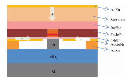
Hong T, Ran G Z, Chen T, et al. A selective-area metal bonding InGaAsP-Si laser. IEEE Photon Technol Lett, 2010, 22(15): 1141 doi: 10.1109/LPT.2010.2050683 |
| [29] |
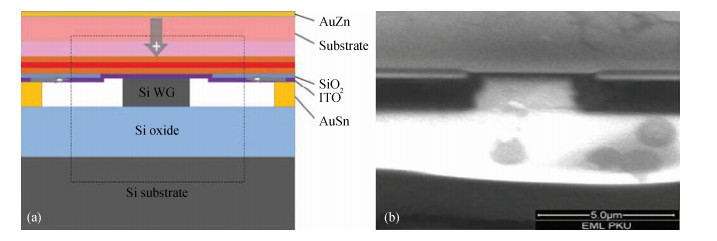
Hong T, Li Y P, Chen W X, et al. Bonding InGaAsP/ITO/Si hybrid laser with ITO as cathode and light-coupling material. IEEE Photon Technol Lett, 2012, 24(8): 712 doi: 10.1109/LPT.2012.2187328 |
| [30] |
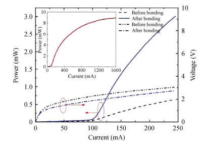
Yuan Lei, Tao Li, Yu Haoyong, et al. Hybrid InGaAsP-Si evanescent laser by selective-area metal-bonding method. IEEE Photonics Technology Letters, 2013, 25(12): 1180 doi: 10.1109/LPT.2013.2262265 |
| [31] |
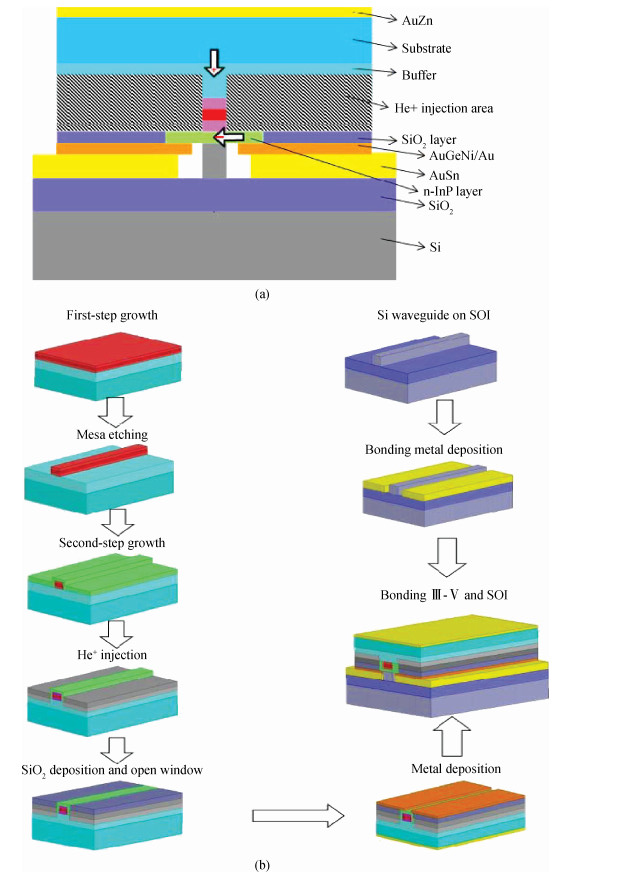
Yuan Lijun, Tao Li, Chen Weixi, et al. A buried ridge stripe structure InGaAsP-Si hybrid laser. IEEE Photonics Technology Letters, 2015, 27(4): 352 doi: 10.1109/LPT.2014.2372892 |
| [32] |
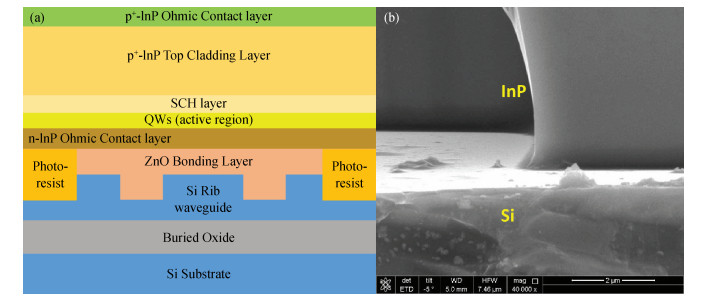
Huang Xinnan, Gao Yonghao, Xu Xingsheng. Bonding III-V material to SOI with transparent and conductive ZnO film at low temperature. Optics Express, 2014, 22(12): 14285 doi: 10.1364/OE.22.014285 |


 DownLoad: