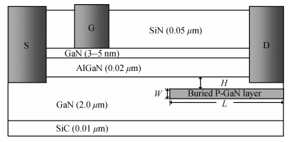
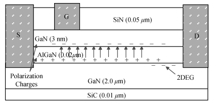
Fig. 1.
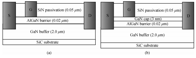
Schematic of HEMT. (a) Conventional GaN HEMT. (b) GaN/AlGaN/GaN HEMT.
SEMICONDUCTOR DEVICES
Yang Liu, Changchun Chai, Chunlei Shi, Qingyang Fan and Yuqian Liu
Corresponding author: Liu Yang, Email:lliu_yang@163.com
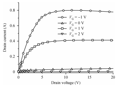
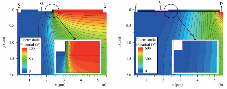
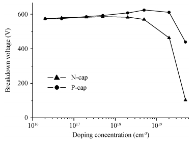
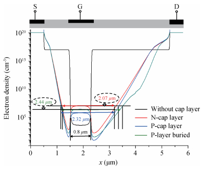
Abstract: Simulations are carried out to explore the possibility of achieving high breakdown voltage of GaN HEMT (high-electron mobility transistor). GaN cap layers with gradual increase in the doping concentration from 2×10¹⁶ to 5×1019 cm-3 of N-type and P-type cap are investigated, respectively. Simulation results show that HEMT with P-doped GaN cap layer shows more potential to achieve higher breakdown voltage than N-doped GaN cap layer under the same doping concentration. This is because the ionized net negative space charges in P-GaN cap layer could modulate the surface electric field which makes more contribution to RESURF effect. Furthermore, a novel GaN/AlGaN/GaN HEMT with P-doped GaN buried layer in GaN buffer between gate and drain electrode is proposed. It shows enhanced performance. The breakdown voltage of the proposed structure is 640 V which is increased by 12% in comparison to UID (un-intentionally doped) GaN/AlGaN/GaN HEMT. We calculated and analyzed the distribution of electrons' density. It is found that the depleted region is wider and electric field maximum value is induced at the left edge of buried layer. So the novel structure with P-doped GaN buried layer embedded in GaN buffer has the better improving characteristics of the power devices.
Keywords: GaN HEMT, optimization design, breakdown voltage, cap layer
| [1] |
Kizilbey O. Highly efficient 2.7-2.9 GHz class-F and inverse class-F power amplifiers in GaN HEMT technology. IEICE Electronics Express, 2013, 10 (7): 20130132 doi: 10.1587/elex.10.20130132
|
| [2] |
Kizilbey O, Palamutçuogullari O, Yarman S B. 3.5-3.8 GHz class-E balanced GaN HEMT power amplifier with 20 W Pout and 80% PAE. IEICE Electronics Express, 2013, 10 (5): 20130104 doi: 10.1587/elex.10.20130104
|
| [3] |
Zhan Teng, Zhang Yang, Li Jing, et al. The design and fabrication of a GaN-based monolithic light-emitting diode array. Journal of Semiconductors, 2013, 34(9): 094010 doi: 10.1088/1674-4926/34/9/094010
|
| [4] |
Li Linqing, Lü Yanwu. Surface-plasmon-enhanced light transmission intensity with a basic grating in GaN-based LED. Journal of Semiconductors, 2014, 35(4): 043003 doi: 10.1088/1674-4926/35/4/043003
|
| [5] |
Karmalkar S, Mishra U K. Enhancement of breakdown voltage in AlGaN/GaN high electron mobility transistors using a field plate. IEEE Trans Electron Devices, 2001, 48(8): 1515 doi: 10.1109/16.936500
|
| [6] |
Khan M A, Park H C. Design of normally-off GaN-based T-gate with drain-field-plate (TGDFP) HEMT for power and RF applications. IEICE Electronics Express, 2014, 14 (6): 20140163 https://www.researchgate.net/publication/287308834_Design_of_normally-off_GaN-based_T-gate_with_Drain-Field-Plate_TGDFP_HEMT_for_power_and_RF_applications
|
| [7] |
Choi Y C, Pophristic M, Cha H Y, et al. The effect of an Fe-doped GaN buffer on off-state breakdown characteristics in AlGaN/GaN HEMTs on Si substrate. IEEE Trans Electron Devices, 2006, 53 (12): 2926 doi: 10.1109/TED.2006.885679
|
| [8] |
Selvaraj S L, Suzue T, Egawa T. Breakdown enhancement of AlGaN/GaN HEMTs on 4-in silicon by improving the GaN quality on thick buffer layers. IEEE Electron Device Lett, 2009, 30(6): 587 doi: 10.1109/LED.2009.2018288
|
| [9] |
Arulkumaran S, Egawa T, Matsui S, et al. Enhancement of breakdown voltage by AlN buffer layer thickness in AlGaN/GaN high-electron-mobility transistors on 4 in diameter silicon. Appl Phys Lett, 2005, 86: 123503 doi: 10.1063/1.1879091
|
| [10] |
Visalli D, Van Hove M, Derluyn J, et al. AlGaN/GaN/AlGaN double heterostructures on silicon substrates for high breakdown voltage field-effect transistors with low on-resistance. Jpn J Appl Phys, 2009 48: 04C101 https://www.researchgate.net/publication/243748756_AlGaNGaNAlGaN_Double_Heterostructures_on_Silicon_Substrates_for_High_Breakdown_Voltage_Field-Effect_Transistors_with_low_On-Resistance
|
| [11] |
Lee H S, Piedra D, Sun M, et al. 3000 V 4.3 mΩ·cm2 InAlN/GaN MOSHEMTs with AlGaN back barrier. IEEE Electron Device Lett, 2012, 33(7): 982 doi: 10.1109/LED.2012.2196673
|
| [12] |
Oguzman I H, Bellotti E, Brennan K F, et al. Theory of hole initiated impact ionization in bulk zincblende and wurtzite GaN. J Appl Phys, 1997, 81: 7827 doi: 10.1063/1.365392
|
| [13] |
Liu G, Wu J, Lu Y, et al. A theoretical calculation of the impact of GaN cap and AlxGa1-xN barrier thickness fluctuations on two-dimensional electron gas in a GaN/AlxGa1-xN/GaN heterostructure. IEEE Trans Electron Devices 2011, 58(12): 4272 doi: 10.1109/TED.2011.2167334
|
| [14] |
Zhao J T, Lin Z J, Luan C B, et al. Effects of GaN cap layer thickness on an AlN/GaN heterostructure. Chin Phys B, 2014, 23(12): 127104 doi: 10.1088/1674-1056/23/12/127104
|
| [15] |
Ambacher O, Foutz B, Smart J, et al. Two dimensional electron gases induced by spontaneous and piezoelectric polarization in undoped and doped AlGaN/GaN heterostructures. J Appl Phys, 2000, 87(1): 334 doi: 10.1063/1.371866
|
| [16] |
Bardeen J, Shockley W. Deformation potentials and mobilities in non-polar crystals. Phys Rev, 1950, 80(1): 72 doi: 10.1103/PhysRev.80.72
|
| [17] |
Arulkumaran S, Egawa, T Ishikawa H. Studies on the influences of i-GaN, n-GaN, p-GaN and InGaN cap layers in AlGaN/GaN high-electron-mobility transistors. Jpn J Appl Phys, 2005, 44(1): 2953 https://www.researchgate.net/publication/243743843_Studies_on_the_influences_of_i-GaN_n-GaN_p-GaN_and_InGaN_cap_layers_in_AlGaNGaN_high-electron-mobility_transistors
|
| [18] |
Lim J Y, Choi Y H, Cho K H, et al. 1.4 kV AlGaN/GaN HEMTs employing As+ ion implantation on SiO2 passivation layer. Power Electronics Specialists Conference, 2008: 88 http://ieeexplore.ieee.org/xpls/abs_all.jsp?arnumber=4591904
|
| [19] |
Cho K H, Choi Y H, Lim J Y, et al. Increase of breakdown voltage on AlGaN/GaN HEMTs by employing proton implantation. IEEE Trans Electron Devices, 2009, 56(3): 365 doi: 10.1109/TED.2008.2011931
|
| [20] |
Fu Binglei, Liu Naixin, Liu Zhe, et al. Advantages of InGaN/GaN light emitting diodes with p-GaN grown under high pressure. Journal of Semiconductors, 2014, 35(11): 114007 doi: 10.1088/1674-4926/35/11/114007
|
| [21] |
Duan B X, Zhang B, Li Z J. New thin-film power MOSFETs with a buried oxide double step structure. IEEE Electron Device Lett, 2006, 27(5): 377 doi: 10.1109/LED.2006.872904
|
| [22] |
Li Q, Li Z J. Analytical model for surface electrical field distribution of LDD power devices. Microelectronics, 2007, 37(3): 309 http://cn.bing.com/academic/profile?id=2126079244&encoded=0&v=paper_preview&mkt=zh-cn
|


Article views: 4823 Times PDF downloads: 102 Times Cited by: 0 Times
Received: 19 April 2016 Revised: 14 July 2016 Online: Published: 01 December 2016
| Citation: |
Yang Liu, Changchun Chai, Chunlei Shi, Qingyang Fan, Yuqian Liu. Optimization design on breakdown voltage of AlGaN/GaN high-electron mobility transistor[J]. Journal of Semiconductors, 2016, 37(12): 124002. doi: 10.1088/1674-4926/37/12/124002
****
Y Liu, C C Chai, C L Shi, Q Y Fan, Y Q Liu. Optimization design on breakdown voltage of AlGaN/GaN high-electron mobility transistor[J]. J. Semicond., 2016, 37(12): 124002. doi: 10.1088/1674-4926/37/12/124002.

|
| [1] |
Kizilbey O. Highly efficient 2.7-2.9 GHz class-F and inverse class-F power amplifiers in GaN HEMT technology. IEICE Electronics Express, 2013, 10 (7): 20130132 doi: 10.1587/elex.10.20130132
|
| [2] |
Kizilbey O, Palamutçuogullari O, Yarman S B. 3.5-3.8 GHz class-E balanced GaN HEMT power amplifier with 20 W Pout and 80% PAE. IEICE Electronics Express, 2013, 10 (5): 20130104 doi: 10.1587/elex.10.20130104
|
| [3] |
Zhan Teng, Zhang Yang, Li Jing, et al. The design and fabrication of a GaN-based monolithic light-emitting diode array. Journal of Semiconductors, 2013, 34(9): 094010 doi: 10.1088/1674-4926/34/9/094010
|
| [4] |
Li Linqing, Lü Yanwu. Surface-plasmon-enhanced light transmission intensity with a basic grating in GaN-based LED. Journal of Semiconductors, 2014, 35(4): 043003 doi: 10.1088/1674-4926/35/4/043003
|
| [5] |
Karmalkar S, Mishra U K. Enhancement of breakdown voltage in AlGaN/GaN high electron mobility transistors using a field plate. IEEE Trans Electron Devices, 2001, 48(8): 1515 doi: 10.1109/16.936500
|
| [6] |
Khan M A, Park H C. Design of normally-off GaN-based T-gate with drain-field-plate (TGDFP) HEMT for power and RF applications. IEICE Electronics Express, 2014, 14 (6): 20140163 https://www.researchgate.net/publication/287308834_Design_of_normally-off_GaN-based_T-gate_with_Drain-Field-Plate_TGDFP_HEMT_for_power_and_RF_applications
|
| [7] |
Choi Y C, Pophristic M, Cha H Y, et al. The effect of an Fe-doped GaN buffer on off-state breakdown characteristics in AlGaN/GaN HEMTs on Si substrate. IEEE Trans Electron Devices, 2006, 53 (12): 2926 doi: 10.1109/TED.2006.885679
|
| [8] |
Selvaraj S L, Suzue T, Egawa T. Breakdown enhancement of AlGaN/GaN HEMTs on 4-in silicon by improving the GaN quality on thick buffer layers. IEEE Electron Device Lett, 2009, 30(6): 587 doi: 10.1109/LED.2009.2018288
|
| [9] |
Arulkumaran S, Egawa T, Matsui S, et al. Enhancement of breakdown voltage by AlN buffer layer thickness in AlGaN/GaN high-electron-mobility transistors on 4 in diameter silicon. Appl Phys Lett, 2005, 86: 123503 doi: 10.1063/1.1879091
|
| [10] |
Visalli D, Van Hove M, Derluyn J, et al. AlGaN/GaN/AlGaN double heterostructures on silicon substrates for high breakdown voltage field-effect transistors with low on-resistance. Jpn J Appl Phys, 2009 48: 04C101 https://www.researchgate.net/publication/243748756_AlGaNGaNAlGaN_Double_Heterostructures_on_Silicon_Substrates_for_High_Breakdown_Voltage_Field-Effect_Transistors_with_low_On-Resistance
|
| [11] |
Lee H S, Piedra D, Sun M, et al. 3000 V 4.3 mΩ·cm2 InAlN/GaN MOSHEMTs with AlGaN back barrier. IEEE Electron Device Lett, 2012, 33(7): 982 doi: 10.1109/LED.2012.2196673
|
| [12] |
Oguzman I H, Bellotti E, Brennan K F, et al. Theory of hole initiated impact ionization in bulk zincblende and wurtzite GaN. J Appl Phys, 1997, 81: 7827 doi: 10.1063/1.365392
|
| [13] |
Liu G, Wu J, Lu Y, et al. A theoretical calculation of the impact of GaN cap and AlxGa1-xN barrier thickness fluctuations on two-dimensional electron gas in a GaN/AlxGa1-xN/GaN heterostructure. IEEE Trans Electron Devices 2011, 58(12): 4272 doi: 10.1109/TED.2011.2167334
|
| [14] |
Zhao J T, Lin Z J, Luan C B, et al. Effects of GaN cap layer thickness on an AlN/GaN heterostructure. Chin Phys B, 2014, 23(12): 127104 doi: 10.1088/1674-1056/23/12/127104
|
| [15] |
Ambacher O, Foutz B, Smart J, et al. Two dimensional electron gases induced by spontaneous and piezoelectric polarization in undoped and doped AlGaN/GaN heterostructures. J Appl Phys, 2000, 87(1): 334 doi: 10.1063/1.371866
|
| [16] |
Bardeen J, Shockley W. Deformation potentials and mobilities in non-polar crystals. Phys Rev, 1950, 80(1): 72 doi: 10.1103/PhysRev.80.72
|
| [17] |
Arulkumaran S, Egawa, T Ishikawa H. Studies on the influences of i-GaN, n-GaN, p-GaN and InGaN cap layers in AlGaN/GaN high-electron-mobility transistors. Jpn J Appl Phys, 2005, 44(1): 2953 https://www.researchgate.net/publication/243743843_Studies_on_the_influences_of_i-GaN_n-GaN_p-GaN_and_InGaN_cap_layers_in_AlGaNGaN_high-electron-mobility_transistors
|
| [18] |
Lim J Y, Choi Y H, Cho K H, et al. 1.4 kV AlGaN/GaN HEMTs employing As+ ion implantation on SiO2 passivation layer. Power Electronics Specialists Conference, 2008: 88 http://ieeexplore.ieee.org/xpls/abs_all.jsp?arnumber=4591904
|
| [19] |
Cho K H, Choi Y H, Lim J Y, et al. Increase of breakdown voltage on AlGaN/GaN HEMTs by employing proton implantation. IEEE Trans Electron Devices, 2009, 56(3): 365 doi: 10.1109/TED.2008.2011931
|
| [20] |
Fu Binglei, Liu Naixin, Liu Zhe, et al. Advantages of InGaN/GaN light emitting diodes with p-GaN grown under high pressure. Journal of Semiconductors, 2014, 35(11): 114007 doi: 10.1088/1674-4926/35/11/114007
|
| [21] |
Duan B X, Zhang B, Li Z J. New thin-film power MOSFETs with a buried oxide double step structure. IEEE Electron Device Lett, 2006, 27(5): 377 doi: 10.1109/LED.2006.872904
|
| [22] |
Li Q, Li Z J. Analytical model for surface electrical field distribution of LDD power devices. Microelectronics, 2007, 37(3): 309 http://cn.bing.com/academic/profile?id=2126079244&encoded=0&v=paper_preview&mkt=zh-cn
|

 WeChat ID
Journal of Semiconductors © 2017 All Rights Reserved 京ICP备05085259号-2

 DownLoad: