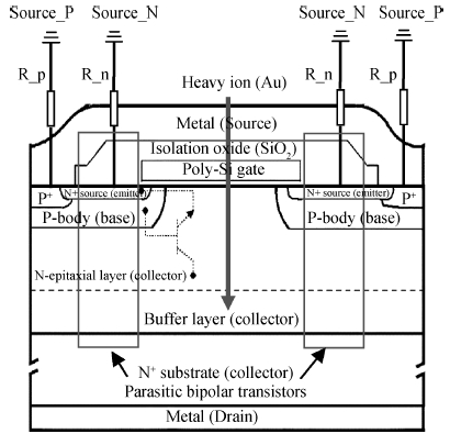
Processing math: 100%
J. Semicond. > 2016, Volume 37 > Issue 2 > 024008

SEMICONDUCTOR DEVICES

Simulation study on single event burnout in linear doping buffer layer engineered power VDMOSFET

Jia Yunpeng1, Su Hongyuan1, Jin Rui2, Hu Dongqing1 and Wu Yu1

+ Author Affiliations
DOI: 10.1088/1674-4926/37/2/024008

PDF

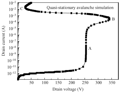
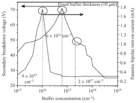
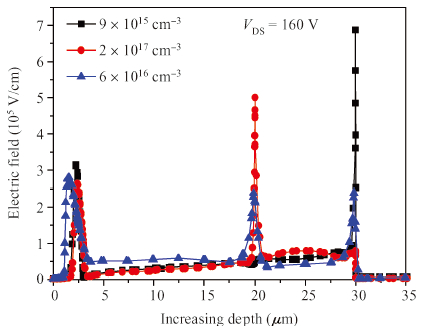
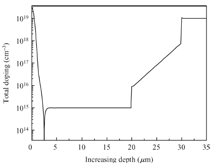
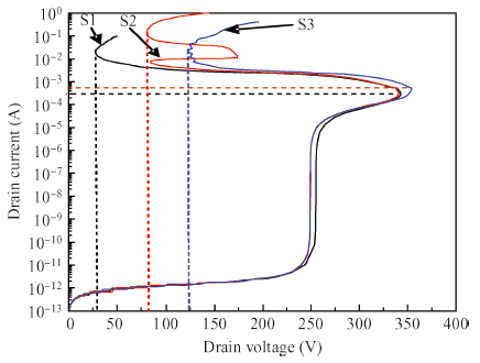
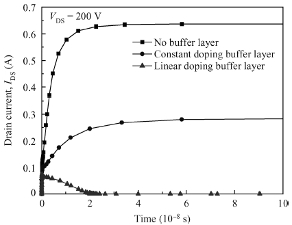
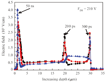
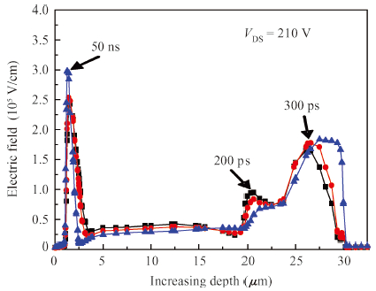
Abstract: The addition of a buffer layer can improve the device's secondary breakdown voltage, thus, improving the single event burnout (SEB) threshold voltage. In this paper, an N type linear doping buffer layer is proposed. According to quasi-stationary avalanche simulation and heavy ion beam simulation, the results show that an optimized linear doping buffer layer is critical. As SEB is induced by heavy ions impacting, the electric field of an optimized linear doping buffer device is much lower than that with an optimized constant doping buffer layer at a given buffer layer thickness and the same biasing voltages. Secondary breakdown voltage and the parasitic bipolar turn-on current are much higher than those with the optimized constant doping buffer layer. So the linear buffer layer is more advantageous to improving the device's SEB performance.

Key words: single event burnout (SEB)quasi-static avalanchelinear doping buffer layerheavy ion Au beam

Low-dimensional quantum well (QW) structures can be manufactured by the advanced growth of molecular-beam epitaxy (MBE)[1], chemical-vapor deposition (CVD)[2] and chemical lithography (CL)[3] techniques. Using these techniques, the growth of QW structures with controllable thickness has become possible. These semiconductor structures have stimulated new works in the field of semiconductor physics over the past years. Through the experiments, Negoita and Snoke[4] developed the harmonic-potential traps of indirect excitons with Bose condensation in two-dimensional coupled QWs. With the lateral periodic potential, Nomura et al.[5] demonstrated Fermi-edge singularities in the n-type modulation-doped QWs' photoluminescence spectra. Using the interference of orthogonal surface acoustic wave beams, Alsina[6] realized the dynamic dots consisting of the confined and mobile potentials in GaAs QWs. Recently, the problems of quantum information processing (QIP) and quantum computation (QC) in semiconductor nanostructures have been studied. In the experiments, Clausen et al.[7] reported the photonic entanglement quantum storage in a crystal. For scalable QC with ultra-cold atoms in the optical lattices, Weitenberg et al.[8] present the complete architecture employing the optical tweezers focused to the lattice spacing size. Alicea et al.[9] showed the non-Abelian statistics and the topological QC in one-dimensional wire networks. In the aspect of theories, Ferrón et al.[10] achieved the control model qubit in a multi-layered quantum dot (QD). Jordan et al.[11] developed the quantum algorithms problems of quantum field theories. Zhang et al.[12] studied the genetic design of spin qubit which enhanced valley splitting in silicon QW. Actually, the polaron properties of QW with different confinement potentials, take for example the parabolic, hyperbolic, exponential, Wood-Saxon, Morse potential, pseudo harmonic and Gaussian potentials, have been investigated by the experimental and theoretical researchers. Recently, with the effective mass approximation (EMA), the compact density matrix theory and the iterative approach, Zhai[13] studied the second-harmonic generation induced electric field in AGPQWs. By the EMA and the perturbation theory, Wu et al.[14] theoretically presented the polaron effects on nonlinear optical rectification with applied electric field in the AGPQWs. Ma et al.[15] used linear combination operator and unitary transformation methods to study magnetic field effects on the vibrational frequency, the ground state and binding energy of weak-coupling polaron in GaAs AGPQW. With Coulombic impurity field, electric field and magnetic field, Xiao et al.[16], Xiao[17] and Cai et al.[18] investigated the AGPQW qubit effect. However, the reports about the investigations of qubit properties in AGPQW are seldom, which is one of the motivations of the present paper. We obtain the properties of the AGPQW qubit in RbCl crystal and indicated some ways for decoherence suppression changing the AGPQW's physical quantities. Our results using the actual semiconductor RbCl crystal are vitally important for low-dimensional nanomaterial science and quantum information computation (QIC).

An electron moves in the RbCl crystal AGPQW and interacts with bulk LO phonons. Within the framework of EMA, the system Hamiltonian of electron-phonon interaction can be written as

$ H=p22m+V(z)+qωLOa+qaq+q[Vqaqexp(iqr)+h.c], $

(1)

where

$ \left\{ V(z)={V0exp(z22R2),z0,z<0Vq=i(ωLOq)(2mωLO)1/4(4παV)1/2,α=(e22ωLO)(2mωLO)1/2(1ε1ε0), \right. $

(2)

With m being the electron band mass, aq+(aq) denoting the bulk LO phonon creation (annihilation) operator and q response wave vector. Also, p and r are the momentum and the electron position vector. The V (z) z-direction potential represents the QWs growth direction[19, 20]. V0 and R are the AGPQW height and the Gaussian potential range, respectively. Following the VMPT[21-23], the strong-coupling polaron trial wavefunction can divide into two parts: describing the electron and describing the phonon. So the trial wavefunction can be represented as

$ \left| \Psi \right\rangle {\rm{ = }}\left| \varphi \right\rangle U\left| {{0_{ph}}} \right\rangle . $

(3)

$\left|\varphi \right\rangle $ relates only to the electron coordinate, $U\left|0_{ph} \right\rangle $ and $\left| 0_{ph}\right\rangle$ represents respectively the phonon coherent state and the phonon vacuum state,

$ U = \exp \left[{\sum\limits_\mathit{\boldsymbol{q}} {\left( {a_\mathit{\boldsymbol{q}}^ + {f_q}-{a_\mathit{\boldsymbol{q}}}f_q^ * } \right)} } \right]. $

(4)

$f_{q} (f_{q}^{\ast } )$ is the variational function. We may choose the trial GFES wave-functions[18, 19] of the electron to be

$ \left| {\varphi ({\lambda _0})} \right\rangle = \left| 0 \right\rangle \left| {{0_{ph}}} \right\rangle = {\pi ^{\frac{3}{4}}}\lambda _0^{\frac{3}{2}}\exp \left[{-\frac{{\lambda _0^2{r^2}}}{2}} \right]\left| {{0_{ph}}} \right\rangle, $

(5)

$ |φ(λ0)=|1|0ph=(π34)14λ521rcosθexp(λ21r22)exp(±iϕ)|0ph, $

(6)

where $\lambda_{0} $ and $\lambda_{1} $ are the variational parameters.

Then, minimizing the Hamiltonian expectation value, we obtain the polaron ground and first excited states' energies $E_{0} =\left\langle {\phi_{0}} \right|{H}'\left|\phi_{0} \right\rangle$ and $E_{1} =\left\langle {\phi_{1}}\right|{H}'\left| \phi_{0}\right\rangle$. The electron's two state energies in the AGPQW can be shown as

$ {E_0}\left( {{\lambda _0}} \right) = \frac{{3{\hbar ^2}}}{{4m}}\lambda _0^2-{V_0}{\left( {1 + \frac{1}{{2\lambda _0^2{R^2}}}} \right)^{-\frac{1}{2}}}-\frac{{\sqrt 2 }}{{\sqrt \pi }}\alpha \hbar {\omega _{{\rm{LO}}}}{\lambda _0}{r_0}, $

(7)

$ {E_1}\left( {{\lambda _1}} \right) = \frac{{5{\hbar ^2}}}{{4m}}\lambda _1^2-{V_0}{\left( {1 + \frac{1}{{2\lambda _1^2{R^2}}}} \right)^{-\frac{3}{2}}}-\frac{{3\sqrt 2 }}{{4\sqrt \pi }}\alpha \hbar {\omega _{{\rm{LO}}}}{\lambda _1}{r_0}, $

(8)

The quantity ${r_0} = {\left( {\hbar /2m{\omega _{{\rm{LO}}}}} \right)^{1/2}}$ is the polaron radius. Using the variational method, then, we will get the two-energy-level and levels-functions. So, we are building up a single qubit of two-level system. The electron superposition state and its time evolution can be expressed as

$ \left| {{\Psi _{01}}} \right\rangle = \frac{1}{{\sqrt 2 }}(\left| 0 \right\rangle + \left| 1 \right\rangle ), $

(9)

$ ψ01(r,t)=12ψ0(r)exp(iE0t)+12ψ1(r)exp(iE1t). $

(10)

The electron probability density is in the form

$ Q(r,t)=|ψ01(r,t)|2=12[|ψ0(r)|2+|ψ1(r)|2+ψ0(r)ψ1(r)exp(iω01t)+ψ0(r)ψ1(r)exp(iω01t)]. $

(11)

In the above equation, $\omega_{01} ={\left( {E_{1} -E_{0} } \right)} /\hbar $ is the transition frequency. The oscillatory period of probability density is

$ {T_0} = \frac{h}{{{E_1}-{E_0}}}. $

(12)

With the purpose of closing to the actual situation, the experimental parameters of RbCl crystal of $\hbar \omega_{\rm LO} =21.45$ meV, $m=0.432 m_{0} $, $\alpha =3.81$ are used in the calculations. The numerical calculations are presented in Figs. 1-4.

Figure  1.  Probability density Q(x, t, T0=22.475 fs) versus time t and coordinates x.
Figure  2.  Probability density Q(y, t, T0=22.475 fs) versus time t and coordinates y.
Figure  3.  Probability density Q(z, t, T0=22.475 fs) versus time t and coordinates z.
Figure  4.  Oscillating period T0 versus AGPQW height V0 and polaron radius r0.

Fig. 1 shows that the probability density $Q\left( {x, t, T_{0} =22.475}\ {\rm fs}\right)$ changes with time t and different coordinate x in the electrons' superposition state for V0=1.0 meV, R=1.0 nm, r0=2.0 nm, y=0.45 nm and z=0.45 nm. Fig. 2 displays the Q(y, t, T0=22.475 fs) changes with time t and different coordinate y for V0 meV, R=1.0 nm, r0=2.0 nm, x=0.45 nm and z=0.45 nm. Fig. 3 illustrates the Q(z, t, T0=22.475 fs) changes with time t and different coordinate z for V0 meV, R=1.0 nm, r0=2.0 nm, x=0.45 nm and y=0.45 nm. From the setting values and Fig. 1, Fig. 2 and Fig. 3, the identical AGPQW height, the confinement potential range and the polaron radius, and then, the changes of different coordinate, cause the difference of electron probability density. From Figs. 1 and 2, the electron probability density not only oscillates with a central oscillating period T0=22.475 fs in the AGPQW but also varies with the time and different x, y coordinates. Moreover, due to the two-dimensional symmetric structure in the x-y plane of AGPQW, the demonstration of probability density is only single peak configuration. This case is similar to that of the parabolic QD in Refs. [24, 25]. From Fig. 3, the probability density varies differently with respect to the coordinate z than with the x, y coordinates. Moreover, due to the growth direction AGP in the QW, the electron probability density also shows one peak and oscillates with a central oscillating period in the range of z>0, whereas it equals zero for z < 0.

Fig. 4 depicts the oscillating period T0 in relation to the AGPQW height V0 and the polaron radius r0 for R=1.0 nm. From Fig. 4, the oscillating period decreases with the increase of the AGPQW height and the polaron radius. This is because the impacts of the increase of AGPQW height and polaron radius are weaker in the first-excited state than in the ground-state. For this reason, the increasing of AGPQW height and polaron radius causes the increases of energy space between the GFES, whereas it leads to the decrease of oscillating period.

Fig. 5 implies the oscillating period T0 as a relation of the AGPQW height V0 and the confinement potential R for r0=2.0 nm. In Fig. 5, the oscillating period T0 is a decreasing function in the confinement potential for R < 0.24 nm, whereas it is an increasing one for R>0.24 nm, and it is a minimum when R=0.24 nm. It is the characteristic reason that the potential locates in the AGPQW growth direction.

Figure  5.  Oscillating period T0 versus AGPQW height V0 and confinement potential range R.

Adjusting the probability density and its oscillating period changes the following physical quantities: the AGPQW height, the confinement potential, and the polaron radius. With prolonging the qubit life, these are some ways for suppression of de-coherence. Its numerical consequences not only have potential application value in the semiconductor science research field and quantum devices designing, but also are important for QIC.

Based on the VMPT, the probability density versus the time and coordinates, moreover the oscillatory period relates to the AGPQW height, confinement potential and polaron radius. It is indicated that (i) the probability density oscillates periodically in the AGPQW with a certain period T0=22.475 fs; (ii) for the AGP in AGPQW growth direction and the two dimensional symmetric confinement structure in the x, y plane of AGPQW, the probability density is only one peak in z>0, whereas it equals to zero in z < 0; (iii) the oscillating period is a decreasing function of the AGPQW height and polaron radius; (iv) the oscillating period is a decreasing one in the confinement potential R < 0.24 nm, whereas it is an increasing one in R>0.24 nm, and it is a minimum value in R=0.24 nm.


[1]
[2]
[3]
[4]
[5]
[6]
[7]
[8]
[9]
[10]
[11]
Fig. 1.  Cross-sectional representation of a vertical power MOSFET where the n+ source acts like the emitter, p-body acts like the base and the epitaxial layer acts like the collector of the inherent parasitic bipolar transistor.

Fig. 2.  The projected range of Au beam simulation.

Fig. 3.  Illustration of relationship between avalanche characteristics and SEB of device (single epitaxial layer).

Fig. 4.  Simulated secondary breakdown voltage and simulated parasitic bipolar turn-on current as a function of the buffer layer doping concentration using a fixed buffer thickness (10 μm).

Fig. 5.  (Color online) The electric field distribution of device with different doping concentrations of buffer layer when the secondary breakdown occurs with biasing voltage: VGS=0 V and VDS=160 V.

Fig. 6.  The concentration distribution of the VDMOSFET with optimized linear doping buffer layer.

Fig. 7.  (Color online) Quasi-static avalanche simulation curves of VDMOSFETs with different buffer layer structures. S1: no buffer layer; S2: optimized constant single buffer layer (h = 10 μm); S3: optimized linear doping buffer layer (h = 10 μm).

Fig. 8.  Simulation curves of IDS and time for the VDMOSFETs with different buffer structures with biasing voltages: VGS = 0 V and VDS = 200 V.

Fig. 9.  (Color online) The electric field distribution curves of VDMOSFET with the constant doping buffer layer (h = 10 μm) at different times with biasing voltage VDS = 200 V.

Fig. 10.  (Color online) The electric field distribution curves of VDMOSFET with the linear doping buffer layer (h =10 μm) at different times with biasing voltage VDS = 200 V.

[1]
[2]
[3]
[4]
[5]
[6]
[7]
[8]
[9]
[10]
[11]
1. Jiang, J., Hu, D., Li, R. et al. Simulation Study on SEB Resistance of Silicon-based RESURF LDMOS Device with Drain Buffer Layer. 2023. doi:10.1109/ICPET59380.2023.10367666
2. Roed, K., Eriksen, D.O., Ceccaroli, B. et al. Isotopic Enriched and Natural SiC Junction Barrier Schottky Diodes Under Heavy Ion Irradiation. IEEE Transactions on Nuclear Science, 2022, 69(7): 1675-1682. doi:10.1109/TNS.2022.3173061
3. Krishnamurthy, S., Kannan, R., Hussin, F.A. Single event burnout hardening of trench shielded power UMOSFET using High-κ dielectrics. Materials Research Express, 2020, 7(3): 035907. doi:10.1088/2053-1591/ab816a
4. Lu, J., Liu, H., Cai, X. et al. Single-event burnout hardening of planar power MOSFET with partially widened trench source. Journal of Semiconductors, 2018, 39(3): 034003. doi:10.1088/1674-4926/39/3/034003
5. Tang, Z., Fu, X., Yang, F. et al. SEGR- and SEB-hardened structure with DSPSOI in power MOSFETs. Journal of Semiconductors, 2017, 38(12): 124006. doi:10.1088/1674-4926/38/12/124006
  • Search

    Advanced Search >>

    GET CITATION

    shu

    Export: BibTex EndNote

    Article Metrics

    Article views: 3284 Times PDF downloads: 52 Times Cited by: 5 Times

    History

    Received: 14 June 2015 Revised: Online: Published: 01 February 2016

    Catalog

      Email This Article

      User name:
      Email:*请输入正确邮箱
      Code:*验证码错误
      Jia Yunpeng, Su Hongyuan, Jin Rui, Hu Dongqing, Wu Yu. Simulation study on single event burnout in linear doping buffer layer engineered power VDMOSFET[J]. Journal of Semiconductors, 2016, 37(2): 024008. doi: 10.1088/1674-4926/37/2/024008 ****J Y peng, S H yuan, J Rui, H D qing, W Yu. Simulation study on single event burnout in linear doping buffer layer engineered power VDMOSFET[J]. J. Semicond., 2016, 37(2): 024008. doi: 10.1088/1674-4926/37/2/024008.
      Citation:
      Jia Yunpeng, Su Hongyuan, Jin Rui, Hu Dongqing, Wu Yu. Simulation study on single event burnout in linear doping buffer layer engineered power VDMOSFET[J]. Journal of Semiconductors, 2016, 37(2): 024008. doi: 10.1088/1674-4926/37/2/024008 ****
      J Y peng, S H yuan, J Rui, H D qing, W Yu. Simulation study on single event burnout in linear doping buffer layer engineered power VDMOSFET[J]. J. Semicond., 2016, 37(2): 024008. doi: 10.1088/1674-4926/37/2/024008.

      Simulation study on single event burnout in linear doping buffer layer engineered power VDMOSFET

      DOI: 10.1088/1674-4926/37/2/024008
      Funds:

      Project supported by the National Natural Science Foundation of China (No. 61176071), the Doctoral Fund of Ministry of Education of China (No. 20111103120016), and the Science and Technology Program of State Grid Corporation of China (No. SGRI-WD-71-13-006).

      • Received Date: 2015-06-14
      • Accepted Date: 2015-08-19
      • Published Date: 2016-01-25

      Catalog

        /

        DownLoad:  Full-Size Img  PowerPoint
        Return
        Return