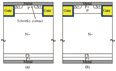
Processing math: 100%
J. Semicond. > 2016, Volume 37 > Issue 2 > 024011

SEMICONDUCTOR DEVICES

A high-conductivity insulated gate bipolar transistor with Schottky hole barrier contact

Mengxuan Jiang1, , Z. John Shen1, Jun Wang1, Xin Yin1, Zhikang Shuai1 and Jiang Lu2

+ Author Affiliations

 Corresponding author: Mengxuan Jiang, Email: mengxuanjiang@qq.com

DOI: 10.1088/1674-4926/37/2/024011

PDF

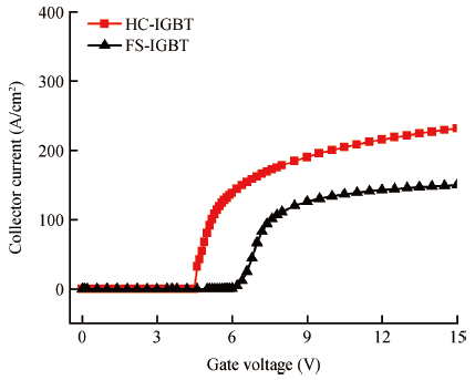
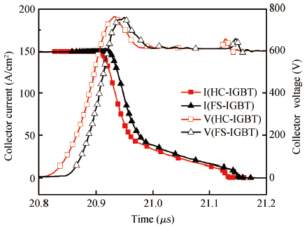
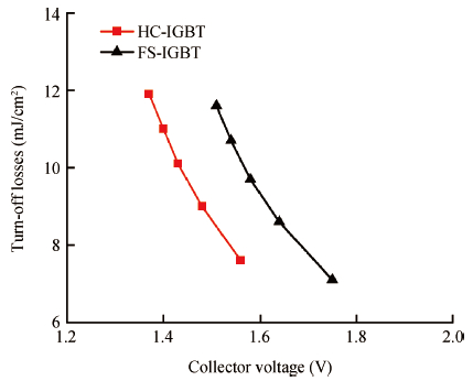
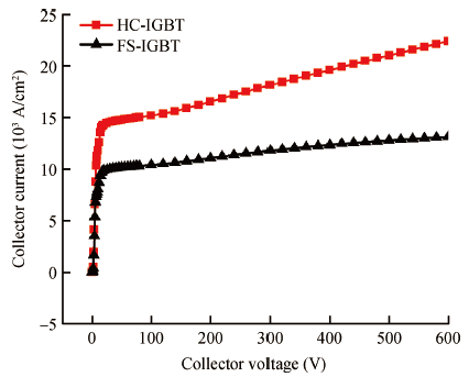
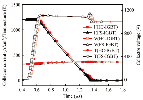
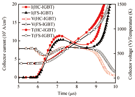
Abstract: This letter proposes a high-conductivity insulated gate bipolar transistor (HC-IGBT) with Schottky contact formed on the p-base, which forms a hole barrier at the p-base side to enhance the conductivity modulation effect. TCAD simulation shows that the HC-IGBT provides a current density increase by 53% and turn-off losses decrease by 27% when compared to a conventional field-stop IGBT (FS-IGBT). Hence, the proposed IGBT exhibits superior electrical performance for high-efficiency power electronic systems.

Key words: breakdown voltageconductivity modulationcurrent densitylatch upIGBT


[1]
[2]
[3]
[4]
[5]
[6]
[7]
[8]
[9]
[10]
[11]
[12]
[13]
[14]
[15]
Fig. 1.  (a) Proposed HC-IGBT and (b) conventional FS-IGBT structures.

Fig. 2.  (Color online) Forward-blocking characteristics of the HC-IGBT and FS-IGBT at a gate voltage of 0 V. The inset of Figure 2 shows the breakdown voltage of the HC-IGBT varies with the work function of the emitter metal.

Fig. 3.  (Color online) Potential distribution of the HC-IGBT and FS-IGBT along the vertical direction between the emitter metal, the n+ source, the p-base, and part of the n-drift region under the avalanche conditions.

Fig. 4.  (Color online) Forward-conduction characteristics of the HC-IGBT and FS-IGBT at a gate voltage of 15 V. The inset of Figure 4 shows the conductivity modulation effect of the HC-IGBT changes with the work function of the emitter metal.

Fig. 5.  (Color online) Potential distribution of the HC-IGBT and FS-IGBT along the vertical direction between the emitter metal, the n+ source, the p-base, and part of the n-drift region at a current density of 150 A/cm2.

Fig. 6.  (Color online) Hole concentration distribution of the HC-IGBT and FS-IGBT along the vertical direction of the n-type drift region at 150 A/cm2.

Fig. 7.  (Color online) Transfer characteristics of the HC-IGBT and FS-IGBT at collector voltage of 1.64 V.

Fig. 8.  (Color online) Turn-off test circuit. The DC bus voltage is set at 600 V, the gate voltage is set at ±15 V, the load current density at 150 A/cm2 and the stray inductance at 60 nH and the gate resistor at 5 Ω.

Fig. 9.  (Color online) Turn-off waveforms of the HC-IGBT and FS-IGBT at a current density of 150 A/cm2, a bus voltage of 600 V, stray inductance of 10 nH and agate voltage of 15 V.

Fig. 10.  Turn-off losses characteristics of the HC-IGBT and FS-IGBT by varying p+ collector concentration at current density of 150 A/cm2, bus voltage of 600 V, gate resistor of 5 Ω and stray inductance of 60 nH.

Fig. 11.  Color online) FBSOA test of the HC-IGBT at gate voltage of 15 V. The conventional FS-IGBT with the same conditions is also included for comparison.

Fig. 12.  (Color online) RBSOA switching waveforms of the HC-IGBT and FS-IGBT at a current density of 1200 A/cm2, a bus voltage of 1000 V, stray inductance of 10 nH and thermal resistance of 20 ℃/cm2kW.

Fig. 13.  (Color online) Short-circuit switching waveforms of the HC-IGBT and FS-IGBT at gate voltage of 15 V, bus voltage of 600 V, gate resistor of 5 Ω, stray inductance of 10 nH and thermal resistance of 20 ℃/cm2kW.

Table 1.   Major device parameters.

DownLoad: CSV
[1]
[2]
[3]
[4]
[5]
[6]
[7]
[8]
[9]
[10]
[11]
[12]
[13]
[14]
[15]
1

Source-field-plated Ga2O3 MOSFET with a breakdown voltage of 550 V

Yuanjie Lü, Xubo Song, Zezhao He, Yuangang Wang, Xin Tan, et al.

Journal of Semiconductors, 2019, 40(1): 012803. doi: 10.1088/1674-4926/40/1/012803

2

Fabrication of 4H-SiC n-channel IGBTs with ultra high blocking voltage

Xiaolei Yang, Yonghong Tao, Tongtong Yang, Runhua Huang, Bai Song, et al.

Journal of Semiconductors, 2018, 39(3): 034005. doi: 10.1088/1674-4926/39/3/034005

3

Modeling on oxide dependent 2DEG sheet charge density and threshold voltage in AlGaN/GaN MOSHEMT

J. Panda, K. Jena, R. Swain, T. R. Lenka

Journal of Semiconductors, 2016, 37(4): 044003. doi: 10.1088/1674-4926/37/4/044003

4

A monolithic integrated low-voltage deep brain stimulator with wireless power and data transmission

Zhang Zhang, Ye Tan, Jianmin Zeng, Xu Han, Xin Cheng, et al.

Journal of Semiconductors, 2016, 37(9): 095003. doi: 10.1088/1674-4926/37/9/095003

5

Theoretical modification of the negative Miller capacitance during the switching transients of IGBTs

Yuan Teng, Yangjun Zhu, Zhengsheng Han, Tianchun Ye

Journal of Semiconductors, 2016, 37(7): 074005. doi: 10.1088/1674-4926/37/7/074005

6

An insulated gate bipolar transistor with surface n-type barrier

Mengxuan Jiang, Z. John Shen, Jun Wang, Zhikang Shuai, Xin Yin, et al.

Journal of Semiconductors, 2015, 36(12): 124004. doi: 10.1088/1674-4926/36/12/124004

7

Experimental and theoretical study of an improved breakdown voltage SOI LDMOS with a reduced cell pitch

Xiaorong Luo, Xiaowei Wang, Gangyi Hu, Yuanhang Fan, Kun Zhou, et al.

Journal of Semiconductors, 2014, 35(2): 024007. doi: 10.1088/1674-4926/35/2/024007

8

Model development for analyzing 2DEG sheet charge density and threshold voltage considering interface DOS for AlInN/GaN MOSHEMT

Devashish Pandey, T.R. Lenka

Journal of Semiconductors, 2014, 35(10): 104001. doi: 10.1088/1674-4926/35/10/104001

9

Breakdown voltage and current collapse of F-plasma treated AlGaN/GaN HEMTs

Chong Wang, Chong Chen, Yunlong He, Xuefeng Zheng, Xiaohua Ma, et al.

Journal of Semiconductors, 2014, 35(1): 014008. doi: 10.1088/1674-4926/35/1/014008

10

Simulating and modeling the breakdown voltage in a semi-insulating GaAs P+N junction diode

A. Resfa, Brahimi.R. Menezla, M. Benchhima

Journal of Semiconductors, 2014, 35(8): 084002. doi: 10.1088/1674-4926/35/8/084002

11

A voltage regulator system with dynamic bandwidth boosting for passive UHF RFID transponders

Jinpeng Shen, Xin'an Wang, Shan Liu, Shoucheng Li, Zhengkun Ruan, et al.

Journal of Semiconductors, 2013, 34(10): 105004. doi: 10.1088/1674-4926/34/10/105004

12

A simulation study on a novel trench SJ IGBT

Wang Bo, Tan Jingfei, Zhang Wenliang, Chu Weili, Zhu Yangjun, et al.

Journal of Semiconductors, 2012, 33(11): 114002. doi: 10.1088/1674-4926/33/11/114002

13

Influence of etching current density on the morphology of macroporous silicon arrays by photo-electrochemical etching

Wang Guozheng, Chen Li, Qin Xulei, Wang Ji, Wang Yang, et al.

Journal of Semiconductors, 2010, 31(7): 074011. doi: 10.1088/1674-4926/31/7/074011

14

Conductivity modulation enhanced lateral IGBT with SiO2 shielded layer anode by SIMOX technology on SOI substrate

Chen Wensuo, Zhang Bo, Li Zhaoji, Fang Jian, Guan Xu, et al.

Journal of Semiconductors, 2010, 31(6): 064004. doi: 10.1088/1674-4926/31/6/064004

15

A novel TFS-IGBT with a super junction floating layer

Ye Jun, Fu Daping, Luo Bo, Zhao Yuanyuan, Qiao Ming, et al.

Journal of Semiconductors, 2010, 31(11): 114008. doi: 10.1088/1674-4926/31/11/114008

16

A 1.8 V LDO voltage regulator with foldback current limit and thermal protection

Liu Zhiming, Fu Zhongqian, Huang Lu, Xi Tianzuo

Journal of Semiconductors, 2009, 30(8): 085007. doi: 10.1088/1674-4926/30/8/085007

17

Realizing High Breakdown Voltage SJ-LDMOS on Bulk Silicon Using a Partial n-Buried Layer

Chen Wanjun, Zhang Bo, Li Zhaoji

Chinese Journal of Semiconductors , 2007, 28(3): 355-360.

18

Breakdown Voltage and Charge to Breakdown Investigation of Gate Oxide of 0.18μm Dual Gate CMOS Process with Different Measurement Methods

Zhao Yi, Wan Xinggong, Xu Xiangming, Cao Gang, Bu Jiao, et al.

Chinese Journal of Semiconductors , 2006, 27(2): 290-293.

19

Low Voltage Flash Memory Cells Using SiGe Quantum Dots for Enhancing F-N Tunneling

Deng Ning, Pan Liyang, Liu Zhihong, Zhu Jun, Chen Peiyi, et al.

Chinese Journal of Semiconductors , 2006, 27(3): 454-458.

20

On-State Breakdown Model for High Voltage RESURF LDMOS

Fang Jian, Yi Kun, Li Zhaoji, and Zhang Bo(436)

Chinese Journal of Semiconductors , 2005, 26(3): 436-442.

  • Search

    Advanced Search >>

    GET CITATION

    Mengxuan Jiang, Z. John Shen, Jun Wang, Xin Yin, Zhikang Shuai, Jiang Lu. A high-conductivity insulated gate bipolar transistor with Schottky hole barrier contact[J]. Journal of Semiconductors, 2016, 37(2): 024011. doi: 10.1088/1674-4926/37/2/024011
    M X Jiang, Z. John Shen, J Wang, X Yin, Z K Shuai, J Lu. A high-conductivity insulated gate bipolar transistor with Schottky hole barrier contact[J]. J. Semicond., 2016, 37(2): 024011. doi: 10.1088/1674-4926/37/2/024011.
    shu

    Export: BibTex EndNote

    Article Metrics

    Article views: 3345 Times PDF downloads: 30 Times Cited by: 0 Times

    History

    Received: 09 November 2015 Revised: Online: Published: 01 February 2016

    Catalog

      Email This Article

      User name:
      Email:*请输入正确邮箱
      Code:*验证码错误
      Mengxuan Jiang, Z. John Shen, Jun Wang, Xin Yin, Zhikang Shuai, Jiang Lu. A high-conductivity insulated gate bipolar transistor with Schottky hole barrier contact[J]. Journal of Semiconductors, 2016, 37(2): 024011. doi: 10.1088/1674-4926/37/2/024011 ****M X Jiang, Z. John Shen, J Wang, X Yin, Z K Shuai, J Lu. A high-conductivity insulated gate bipolar transistor with Schottky hole barrier contact[J]. J. Semicond., 2016, 37(2): 024011. doi: 10.1088/1674-4926/37/2/024011.
      Citation:
      Mengxuan Jiang, Z. John Shen, Jun Wang, Xin Yin, Zhikang Shuai, Jiang Lu. A high-conductivity insulated gate bipolar transistor with Schottky hole barrier contact[J]. Journal of Semiconductors, 2016, 37(2): 024011. doi: 10.1088/1674-4926/37/2/024011 ****
      M X Jiang, Z. John Shen, J Wang, X Yin, Z K Shuai, J Lu. A high-conductivity insulated gate bipolar transistor with Schottky hole barrier contact[J]. J. Semicond., 2016, 37(2): 024011. doi: 10.1088/1674-4926/37/2/024011.

      A high-conductivity insulated gate bipolar transistor with Schottky hole barrier contact

      DOI: 10.1088/1674-4926/37/2/024011
      Funds:

      Project supported by the National High Technology Research and Development Program of China (No. 2014AA052601) and the National Natural Science Foundation of China (No. 51277060).

      More Information
      • Corresponding author: Email: mengxuanjiang@qq.com
      • Received Date: 2015-11-09
      • Accepted Date: 2015-11-30
      • Published Date: 2016-01-25

      Catalog

        /

        DownLoad:  Full-Size Img  PowerPoint
        Return
        Return