Processing math: 100%
J. Semicond. > 2016, Volume 37 > Issue 4 > 044011

SEMICONDUCTOR DEVICES

Thermal analysis in high power GaAs-based laser diodes

Xueqin Gong, Shiwei Feng, Yuan Yue, Junwei Yang and Jingwei Li

+ Author Affiliations

 Corresponding author: Feng Shiwei,Email:shwfeng@bjut.edu.cn

DOI: 10.1088/1674-4926/37/4/044011

PDF

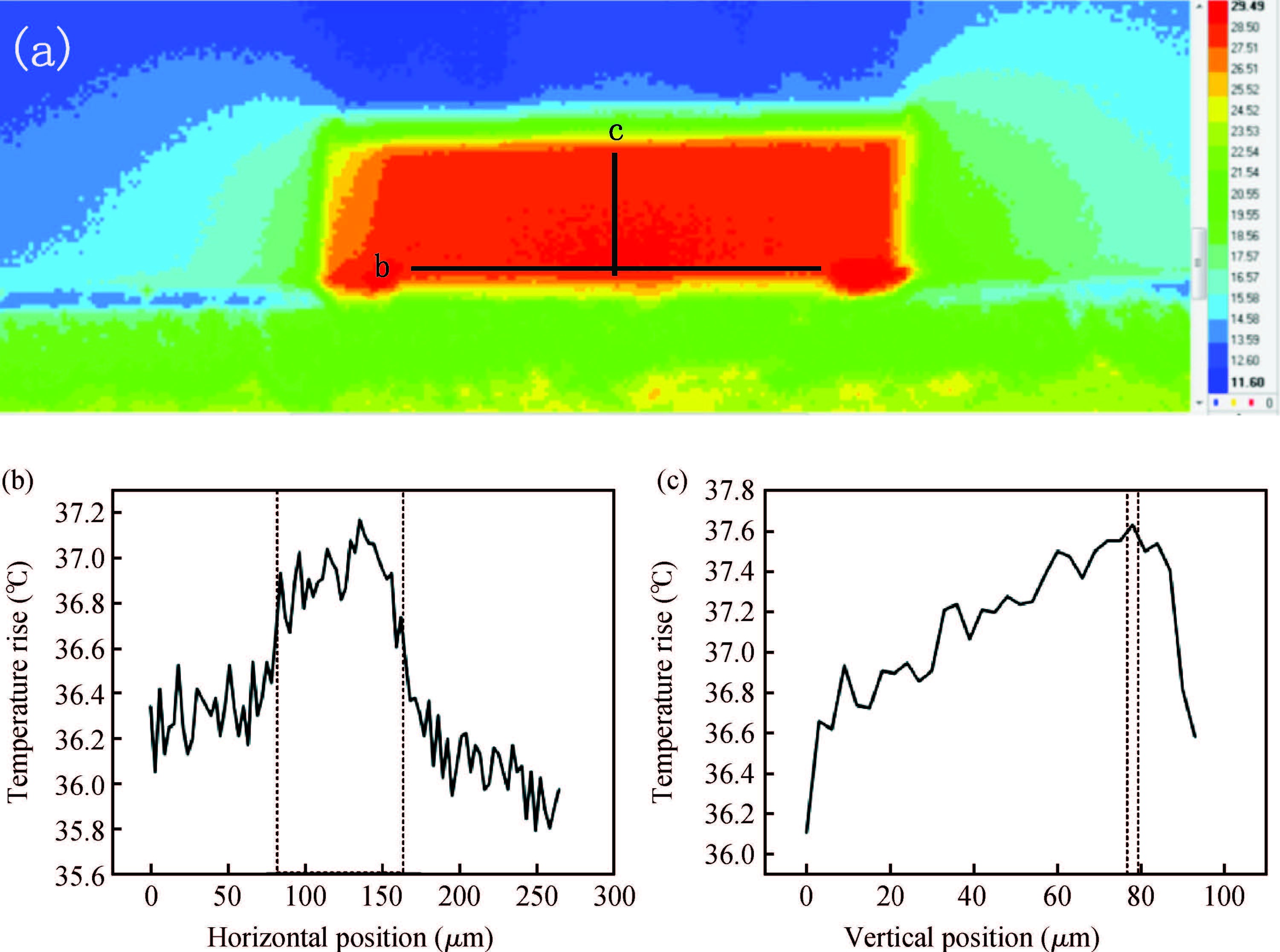
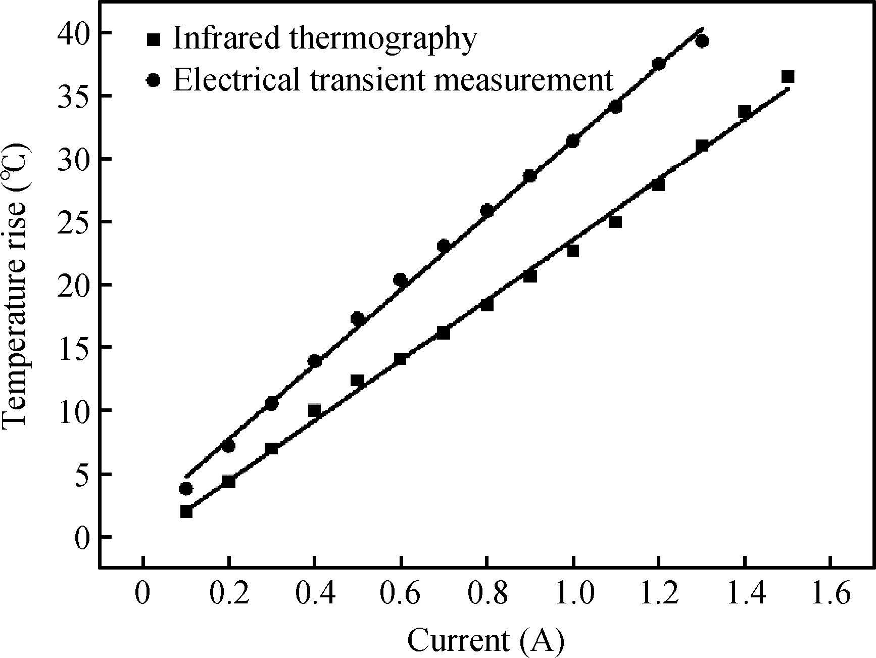
Abstract: The thermal characteristics of 808 nm AlGaAs/GaAs laser diodes (LDs) are analyzed via electrical transient measurements and infrared thermography. The temperature rise and thermal resistance are measured at various input currents and powers. From the electrical transient measurements, it is found that there is a significant reduction in thermal resistance with increasing power because of the device power conversion efficiency. The component thermal resistance that was obtained from the structure function showed that the total thermal resistance is mainly composed of the thermal resistance of the sub-mount rather than that of the LD chip, and the thermal resistance of the sub-mount decreases with increasing current. The temperature rise values are also measured by infrared thermography and are calibrated based on a reference image, with results that are lower than those determined by electrical transient measurements. The difference in the results is caused by the limited spatial resolution of the measurements and by the signal being captured from the facet rather than from the junction of the laser diode.

Key words: laser diodestemperature risethermal resistanceelectrical transient measurementinfrared thermography

Reliable laser diodes (LDs) are required for applications such as materials processing,solid-state laser pumping,optical communications,and printing machines[1]. In recent years,major research efforts have been made to improve the performance of LDs and analyze their reliability. The thermal behavior of LD packaging has been related to the ambient temperature,the base materials,the cooling conditions and the gravity direction[2]. The temperature distribution over the facet of a working device was determined by simulations[3] and spatially resolved thermo-reflectance measurements[4]. Graphene-oxide deposits on the top of p-down-mounted chips have been used to reduce the thermal resistance of high power LDs and improve their upper heat flux removal efficiency[5]. The thermal resistance is the most useful indicator of the thermal performance of LDs[6]. Reduction of the thermal resistance leads to a reduced bulk temperature rise in the LD chip,and the thermal resistance could be reduced by up to 40% by appropriate design of the laser chip and the use of epi-down bonding[7]. The electrically-based transient measurement technique is a popular way to obtain the thermal resistance of LDs and is based on a temperature sensitive parameter[8]. As mentioned above,accurate and reliable characterization of LD thermal behavior has a critical effect on device performance.

In this work,thermal analysis was performed via the electrical transient method and infrared thermography. The electrical method is based on the linear relationship between the junction temperature and the forward voltage. Infrared thermography is a process where original data is calibrated on the basis of emissivity and reference data. Using these two methods,we investigated the thermal resistance and the temperature rise in LDs at various input currents.

Figure 1(a) shows a schematic of the 808 nm GaAs-based LD. The LD mainly consists of the LD chip,indium solder,and a copper heat sink. The LD chip consists of a Zn-doped GaAs cap,a Zn-doped AlGaAs p-cladding layer,an AlGaAs p-guide layer,an AlGaInAs single quantum well (SQW) active area,an AlGaAs n-guide layer,and a Si-doped AlGaAs n-cladding layer. The edge-emitting structure is processed and cleaved to form mirror facets. The facets are coated with anti-reflection (AR)/high-reflectivity (HR) coatings. The cavity length is 2~mm,and the stripe width is 100 μm. The typical lasing wavelength and threshold current are 808 nm and 410 mA,respectively. The power--current--voltage (P--I--V) characteristics during continuous-wave (CW) operation are shown in Figure 1(b).

1.  (a) Schematic of LD structure and (b) PIV characteristic curves of a GaAs-based LD.

The thermal resistance directly indicates the amount of heat that is generated under specific input power levels in a p--n junction and is the most useful indicator of the thermal performance of LDs[2]. According to JEDEC standard No. 51-1[9],the thermal resistance is defined as

Rth=ΔTPt=TjTaPt.
(1)
Here,Pt is the heat dissipated power,Tj is the junction temperature,and Ta is the ambient temperature.

When the laser is operating,the electrical input power will be dissipated as heat and optical power,and thus the apparent thermal resistance is introduced to specify the thermal characteristics. The apparent thermal resistance is defined by the following relation:

Rtha=ΔTPe=ΔTPt+Po=ΔT/Pt1+Po/(PePo)=Rth(1PoPe)=Rth(1η).
(2)
Here,Pe is the electrical input power,Po is the optical power,and η is the power conversion efficiency,which is defined as:
η=PoPe.
(3)

The thermal resistance and the temperature rise in the LD are measured using an electrical transient measurement technique[10] and infrared thermography[11],respectively. The electrical method is based on the linear relationship between junction temperature rise and forward voltage,which is given as follows[12]:

ΔT=ΔVpnk.
(4)
Here,k is a temperature coefficient,and ΔVpn is the difference between the forward voltages before and during operation. We first measured the value of k. The forward voltage is measured at a constant sensor current of 5 mA under various temperatures ranging from 30 to 80 C. We then obtain a proportional constant,as shown in Figure 2(a). The temperature coefficient k is thus 1.7 mV/C. The results clearly show a linear relationship between the temperature and the forward voltage[13].

2.  (a) Forward voltage as a function of temperature at a current of 5 mA and (b) LD temperature rise, thermal resistance and power conversion efficiency as a function of the electrical input power.

The transient thermal resistance is monitored at various input currents over a working current range from 0.1 to 1.3 A. The device is set on a thermoelectric cooler (TEC) and operated at a stabilized temperature of 25 C during the thermal transient measurements. The LD is operated at each working current for 100 s,which is chosen to be sufficiently long to reach a steady state,and is then switched from the working state to a measurement state to measure the forward voltage under a sensor current of 5 mA. The switching process is fast enough and the switch delay time is less than 1 μs. Using Equations (2) and (4),we can obtain both the transient cooling curve and the thermal resistance curve. The transient temperature rise curve is obtained via a mathematical inversion of the transient cooling curve[12].

We have investigated the temperature rise and thermal resistance of the LDs at various input currents. Figure 2(b) shows the LD thermal characteristics,including the junction temperature rise and the apparent thermal resistance of the LD as a function of input power. The temperature rise tends to increase with increasing input power[14]. The apparent thermal resistance falls from 20 to 16.5 C/W over the input power range from 0.15 to 2.3 W,which is in accordance with the characteristic of increasing power conversion efficiency with increasing power,as shown in Figure 2(b). The temperature rise that occurs below the threshold current is caused by Joule heating from the drive current,while significant power-dependent heating caused by absorption of the laser radiation is added to the temperature rise above the threshold current[15]. From Equations (2) and (3),when the input current is beyond the threshold current,the device begins to emit light and the input electrical power is transformed into optical power,and thus the power conversion efficiency begins to increase. When more power is converted into optical power,less is transformed into heat,and thus the apparent thermal resistance begins to decrease. Because of the limitations of the fabrication process,the power conversion efficiency reaches a maximum value after a temperature rise process. In this experiment,we simply consider the case below the maximum power conversion efficiency.

To obtain more information about the heat conduction process,we have analyzed the thermal resistance composition from the transient temperature rise curve using structure functions[16]. Figure 3(a) shows the differential structure function of the LD at a driving current of 0.6 A and the total thermal resistance of the LD is 19 C/W. There are four peaks that correspond to the thermal resistances of the LD chip,the indium solder layer,and the copper sub-mount,and the resistance from the sub-mount to the TEC[12]. From the differential structure function at various currents ranging from 0.4 to 1.3 A,we then abstract the component thermal resistance. The results shown here demonstrate that the total thermal resistance is mainly controlled by the packaging design rather than by the chip structure itself[14, 17],and the decrease in thermal resistance is mainly caused by the decrease in the thermal resistance of the sub-mount.

3.  (Color online) (a) Differential structure function at input current of 0.6 A and (b) component thermal resistance as a function of power.

Temperature distribution images of the entire output facets of working LDs were obtained using an FLIR System SC5700 camera working in the 3.7--4.8-μm range,and a temperature resolution of 20 mK. The thermal infrared camera recorded these images with a frequency of 115 Hz and a spatial resolution of approximately 3.0 μm per pixel. The LD was placed on a TEC that stabilized the heat-sink temperature at 25 C,unless stated otherwise. The LD radiation from the inter-band quantum well transitions was rejected using a Ge wafer as a filter to avoid any additional heating of the lens and the detector during the operation. The system described above is capable of mapping the heat distributions of the facets of LDs during operation. However,the emissivity differences between the elements in the LD,the parasitic reflections of the thermal radiation inside the LD,and the signal interference caused by thermal radiation reflected from surrounding objects are all factors that may cause additional measurement errors and should thus be taken into account[11]. Therefore,to obtain quantitative temperature data,the total thermal measurement system requires a thorough calibration procedure.

The initial calibration process was carried out when the nonoperational LDs were heated by an external heat source in the range from 25 to 55 C in 5 C steps. The temperature was measured using a thermocouple placed in the vicinity of the LDs. For each temperature setting,a thermal image of the device located under a Ge wafer was captured. The calibration characteristics for the typical image regions,i.e.,from the LD facet region and from the heat sink,are shown in Figure 4. The second calibration process includes a reference image of the nonoperational LD acquired at ambient temperature. Subsequently,the LD is switched on and when it is stabilized,the thermal image is captured. The resulting map corresponds to the temperature difference between the reference temperature and the stabilized temperature,as shown in Figure 5(a).

4.  Temperature characteristics for different materials measured using the thermal camera.
5.  (Color online) (a) Thermal image of LD at current of 1.5 A. (b) Horizontal temperature profile and (c) vertical profile of the LD through the active region.

Thermal maps of the LD under various currents ranging from 0.1 to 1.5 A were acquired by following the procedure described above. Figure 5(a) shows the thermal image of an LD operating at a working current of 1.5 A during the second calibration step. Figure 5(b) shows its horizontal profile,taken at line b shown in Figure 5(a),and Figure 5(c) shows its vertical profile,taken at line c in Figure 5(a). Both temperature profiles were measured through the active region after two calibration steps. The width of the active region is approximately 100 μm and the width between the two cladding layers is 1.9 μm,as indicated by the dotted rectangular lines in Figure s 5(b) and 5(c),respectively. We found that the temperature rise in the active region is higher than that which occurs outside the active region[17, 18]. Because the temperature distribution is captured when the device has been stabilized,the temperature of the output facet is almost at its average and the temperature of the active region is only 1--2 C higher than that beyond the active region. The temperature distribution maps of the front output facet were recorded at different driving currents ranging from 0.1 to 1.5 A. The junction temperature difference before and after operation was also acquired. The results shown in Figure 6 demonstrate that the temperature rise at the front facet increased with increasing output power[19] and show the temperature rise characteristics measured by the electrical transient measurement technique and by infrared thermography. The temperature rise value measured by infrared thermography is smaller than that of the transient measurement technique[20, 21]. There are two reasons for this: first,the spatial resolution of the thermographic method is 3 μm,which is far beyond the size of the active region,and thus the thermal images are spatially smoothed. Second,the temperature distribution that was acquired was mainly from the facet rather than the junction and the facet temperature is quite different to that of the junction. In addition,because the material under test,which was AlGaAs or GaAs,is transparent to infrared light,these effects can be caused by residual thermal radiation[11]. Thus,the temperature rise measured by infrared thermography is lower than that obtained by the transient measurement technique. The advantage of infrared thermography is that the temperature rise is measured directly and rapidly,compared with by using a temperature sensitive parameter.

6.  Temperature rise measured by electrical transient measurement and infrared thermography.

The thermal characteristics of 808 nm AlGaAs/GaAs LDs were investigated via electrical transient measurements and infrared thermography. The temperature rise and thermal resistance values of the LDs were measured. The results of the electrical transient measurements demonstrated that the thermal resistance decreases with increasing input power because of the device power conversion efficiency. The structural function was used to analyze the components of the thermal resistance. The results demonstrated that the total thermal resistance is dominated by the sub-mount component rather than that of the LD chip and the thermal resistance of the sub-mount increased with increasing current. The temperature rise that was measured by infrared thermography was smaller than that obtained by the electrical thermal transient,which occurred because of the limited spatial resolution of the measurements and because the signal was captured from the facet rather than from the junction of the LD.


[1]
[2]
[3]
[4]
[5]
[6]
[7]
[8]
[9]
[10]
[11]
[12]
[13]
[14]
[15]
[16]
[17]
[18]
[19]
[20]
[21]
Fig. 1.  (a) Schematic of LD structure and (b) PIV characteristic curves of a GaAs-based LD.

Fig. 2.  (a) Forward voltage as a function of temperature at a current of 5 mA and (b) LD temperature rise, thermal resistance and power conversion efficiency as a function of the electrical input power.

Fig. 3.  (Color online) (a) Differential structure function at input current of 0.6 A and (b) component thermal resistance as a function of power.

Fig. 4.  Temperature characteristics for different materials measured using the thermal camera.

Fig. 5.  (Color online) (a) Thermal image of LD at current of 1.5 A. (b) Horizontal temperature profile and (c) vertical profile of the LD through the active region.

Fig. 6.  Temperature rise measured by electrical transient measurement and infrared thermography.

DownLoad: CSV
DownLoad: CSV
DownLoad: CSV
DownLoad: CSV
[1]
[2]
[3]
[4]
[5]
[6]
[7]
[8]
[9]
[10]
[11]
[12]
[13]
[14]
[15]
[16]
[17]
[18]
[19]
[20]
[21]
1

Effect of microstructure of Au80Sn20 solder on the thermal resistance TO56 packaged GaN-based laser diodes

Hao Lin, Deyao Li, Liqun Zhang, Pengyan Wen, Shuming Zhang, et al.

Journal of Semiconductors, 2020, 41(10): 102104. doi: 10.1088/1674-4926/41/10/102104

2

Al-free cladding-layer blue laser diodes with a low aspect ratio in far-field beam pattern

Meixin Feng, Qian Sun, Jianping Liu, Zengcheng Li, Yu Zhou, et al.

Journal of Semiconductors, 2018, 39(8): 084004. doi: 10.1088/1674-4926/39/8/084004

3

Electrical transport and current properties of rare-earth dysprosium Schottky electrode on p-type GaN at various annealing temperatures

G. Nagaraju, K. Ravindranatha Reddy, V. Rajagopal Reddy

Journal of Semiconductors, 2017, 38(11): 114001. doi: 10.1088/1674-4926/38/11/114001

4

Fabrication of room temperature continuous-wave operation GaN-based ultraviolet laser diodes

Degang Zhao, Jing Yang, Zongshun Liu, Ping Chen, Jianjun Zhu, et al.

Journal of Semiconductors, 2017, 38(5): 051001. doi: 10.1088/1674-4926/38/5/051001

5

Thermal investigation of high-power GaAs-based laser diodes

Jichuan Liu, Cuiluan Wang, Suping Liu, Xiaoyu Ma

Journal of Semiconductors, 2017, 38(5): 054004. doi: 10.1088/1674-4926/38/5/054004

6

Suppression of electron leakage in 808 nm laser diodes with asymmetric waveguide layer

Xiang Li, Degang Zhao, Desheng Jiang, Ping Chen, Zongshun Liu, et al.

Journal of Semiconductors, 2016, 37(1): 014007. doi: 10.1088/1674-4926/37/1/014007

7

GaN-based green laser diodes

Lingrong Jiang, Jianping Liu, Aiqin Tian, Yang Cheng, Zengcheng Li, et al.

Journal of Semiconductors, 2016, 37(11): 111001. doi: 10.1088/1674-4926/37/11/111001

8

Influences of ICP etching damages on the electronic properties of metal field plate 4H-SiC Schottky diodes

Hui Wang, Yingxi Niu, Fei Yang, Yong Cai, Zehong Zhang, et al.

Journal of Semiconductors, 2015, 36(10): 104006. doi: 10.1088/1674-4926/36/10/104006

9

Electrical properties of Ge:Ga near the metal-insulator transition

M Errai, A El Kaaouachi, H El Idrissi

Journal of Semiconductors, 2015, 36(6): 062001. doi: 10.1088/1674-4926/36/6/062001

10

Evaluation of the drain-source voltage effect on AlGaAs/InGaAs PHEMTs thermal resistance by the structure function method

Lin Ma, Shiwei Feng, Yamin Zhang, Bing Deng, Yuan Yue, et al.

Journal of Semiconductors, 2014, 35(9): 094006. doi: 10.1088/1674-4926/35/9/094006

11

Giant magnetoresistance in a two-dimensional electron gas modulated by ferromagnetic and Schottky metal stripes

Lu Jianduo, Xu Bin

Journal of Semiconductors, 2012, 33(7): 074007. doi: 10.1088/1674-4926/33/7/074007

12

Deep submicron PDSOI thermal resistance extraction

Bu Jianhui, Bi Jinshun, Xi Linmao, Han Zhengsheng

Journal of Semiconductors, 2010, 31(9): 094001. doi: 10.1088/1674-4926/31/9/094001

13

High-temperature characteristics of AlxGa1–xN/GaN Schottky diodes

Zhang Xiaoling, Li Fei, Lu Changzhi, Xie Xuesong, Li Ying, et al.

Journal of Semiconductors, 2009, 30(3): 034001. doi: 10.1088/1674-4926/30/3/034001

14

Alloy Temperature Dependence of Offset Voltage and Ohmic Contact Resistance in Thin Base InGaP/GaAs HBTs

Yang Wei, Liu Xunchun, Zhu Min, Wang Runmei, Shen Huajun, et al.

Chinese Journal of Semiconductors , 2006, 27(5): 765-768.

15

Study of Thermal Characteristics of Semiconductor Light-Emitting Devices

Zhang Yuezong, Feng Shiwei, Xie Xuesong, Li Ying, Yang Ji, et al.

Chinese Journal of Semiconductors , 2006, 27(2): 350-353.

16

Temperature Distribution in Ridge Structure InGaN Laser Diodes and Its Influence on Device Characteristics

Li Deyao, Huang Yongzhen, Zhang Shuming, Chong Ming, Ye Xiaojun, et al.

Chinese Journal of Semiconductors , 2006, 27(3): 499-505.

17

Design and Realization of Resonant Tunneling Diodes with New Material Structure

Wang Jianlin, Wang Liangchen, Zeng Yiping, Liu Zhongli, Yang Fuhua, et al.

Chinese Journal of Semiconductors , 2005, 26(1): 1-5.

18

Fabrication of High Power 670nm Laser Diodes

Lin Tao, Jiang Li, Wang Jun, Tan Manqing, Liu Suping, et al.

Chinese Journal of Semiconductors , 2005, 26(S1): 176-179.

19

Material Growth and Device Fabrication of GaN-Based Blue-Violet Laser Diodes

Yang Hui, Chen Lianghui, Zhang Shuming, Chong Ming, Zhu Jianjun, et al.

Chinese Journal of Semiconductors , 2005, 26(2): 414-417.

20

Material Growth and Device Fabrication of GaAs Based 1.3μm GaInNAs Quantum Well Laser Diodes

Chinese Journal of Semiconductors , 2005, 26(9): 1860-1864.

1. Yue, C., Tang, X.-S., Li, Y.-F. et al. Enhanced absorption process in the thin active region of GaAs based p-i-n structure. Chinese Physics B, 2021, 30(9): 097803. doi:10.1088/1674-1056/abfb57
2. Yin, L., Shen, L., Jiang, H. et al. Impact of self-heating effects on nanoscale Ge p-channel FinFETs with Si substrate. Science China Information Sciences, 2018, 61(6): 062401. doi:10.1007/s11432-016-9106-x
3. Rieprich, J., Winterfeldt, M., Kernke, R. et al. Chip-carrier thermal barrier and its impact on lateral thermal lens profile and beam parameter product in high power broad area lasers. Journal of Applied Physics, 2018, 123(12): 125703. doi:10.1063/1.5004503
4. Peng, C., Liu, X.-S., Si, H.-Y. et al. Multi-color Laser Diode Array End-pump Nd:YAG Pulsed Laser. Faguang Xuebao/Chinese Journal of Luminescence, 2018, 39(2): 162-168. doi:10.3788/fgxb20183902.0162
5. Mostallino, R., Garcia, M., Deshayes, Y. et al. Thermal Management Characterization of Microassemblied High Power Distributed-Feedback Broad Area Lasers Emitting at 975nm. Proceedings - Electronic Components and Technology Conference, 2017. doi:10.1109/ECTC.2017.86
6. Mostallino, R., Garcia, M., Deshayes, Y. et al. Thermal management characterization of microassembled high power DFB broad area lasers emitting at 975 nm. 2017. doi:10.1109/HPD.2017.8261099
7. Wang, W., Zhai, T., Wang, H. et al. High Power 1060 nm Distributed Feedback Semiconductor Laser with Double-Trench Ridge Waveguide Structure. Guangzi Xuebao/Acta Photonica Sinica, 2017, 46(6): 0614001. doi:10.3788/gzxb20174606.0614001
8. Yang, J., Zhao, D.-G., Jiang, D.-S. et al. Physical implications of activation energy derived from temperature dependent photoluminescence of InGaN-based materials. Chinese Physics B, 2017, 26(7): 077101. doi:10.1088/1674-1056/26/7/077101
9. Cui, B.-F., Li, S., Kong, Z.-Z. et al. Stable Coupling Efficiency of Semiconductor Lasers with Groove Structure. Faguang Xuebao/Chinese Journal of Luminescence, 2017, 38(5): 636-641. doi:10.3788/fgxb20173805.0636
10. Wang, X., Wang, C., Wu, X. et al. Researching the 915 nm high-power and high-brightness semiconductor laser single chip coupling module. Journal of Semiconductors, 2017, 38(2): 024006. doi:10.1088/1674-4926/38/2/024006
11. Zhao, S., Qi, A., Qu, H. et al. Effect of ridge structure on electro-optical characteristics of ridge-waveguide lasers with low vertical divergence based on photonic crystal structure. Proceedings of SPIE - The International Society for Optical Engineering, 2017. doi:10.1117/12.2284797
12. Li, B., Huang, L., Zhong, M. et al. Direct Vapor Phase Growth and Optoelectronic Application of Large Band Offset SnS2/MoS2 Vertical Bilayer Heterostructures with High Lattice Mismatch. Advanced Electronic Materials, 2016, 2(11): 1600298. doi:10.1002/aelm.201600298
  • Search

    Advanced Search >>

    GET CITATION

    Xueqin Gong, Shiwei Feng, Yuan Yue, Junwei Yang, Jingwei Li. Thermal analysis in high power GaAs-based laser diodes[J]. Journal of Semiconductors, 2016, 37(4): 044011. doi: 10.1088/1674-4926/37/4/044011
    X Q Gong, S W Feng, Y Yue, J W Yang, J W Li. Thermal analysis in high power GaAs-based laser diodes[J]. J. Semicond., 2016, 37(4): 044011. doi: 10.1088/1674-4926/37/4/044011.
    shu

    Export: BibTex EndNote

    Article Metrics

    Article views: 3270 Times PDF downloads: 93 Times Cited by: 12 Times

    History

    Received: 13 June 2015 Revised: Online: Published: 01 April 2016

    Catalog

      Email This Article

      User name:
      Email:*请输入正确邮箱
      Code:*验证码错误
      Xueqin Gong, Shiwei Feng, Yuan Yue, Junwei Yang, Jingwei Li. Thermal analysis in high power GaAs-based laser diodes[J]. Journal of Semiconductors, 2016, 37(4): 044011. doi: 10.1088/1674-4926/37/4/044011 ****X Q Gong, S W Feng, Y Yue, J W Yang, J W Li. Thermal analysis in high power GaAs-based laser diodes[J]. J. Semicond., 2016, 37(4): 044011. doi: 10.1088/1674-4926/37/4/044011.
      Citation:
      Xueqin Gong, Shiwei Feng, Yuan Yue, Junwei Yang, Jingwei Li. Thermal analysis in high power GaAs-based laser diodes[J]. Journal of Semiconductors, 2016, 37(4): 044011. doi: 10.1088/1674-4926/37/4/044011 ****
      X Q Gong, S W Feng, Y Yue, J W Yang, J W Li. Thermal analysis in high power GaAs-based laser diodes[J]. J. Semicond., 2016, 37(4): 044011. doi: 10.1088/1674-4926/37/4/044011.

      Thermal analysis in high power GaAs-based laser diodes

      DOI: 10.1088/1674-4926/37/4/044011
      Funds:

      Project supported by the National Natural Science Foundation of China (Nos. 61376077, 61201046, 61204081).

      More Information
      • Corresponding author: Feng Shiwei,Email:shwfeng@bjut.edu.cn
      • Received Date: 2015-06-13
      • Accepted Date: 2015-09-21
      • Published Date: 2016-01-25

      Catalog

        /

        DownLoad:  Full-Size Img  PowerPoint
        Return
        Return