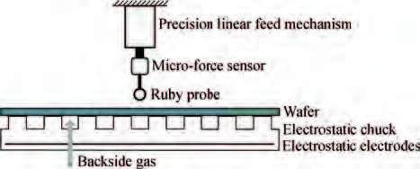
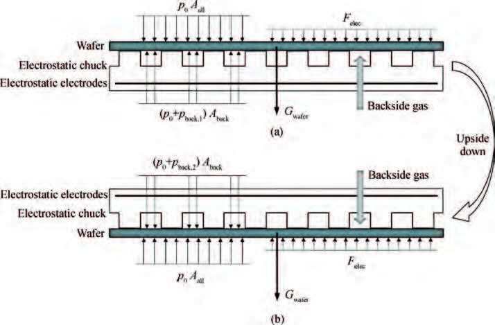
Processing math: 100%
J. Semicond. > 2016, Volume 37 > Issue 4 > 044012

SEMICONDUCTOR DEVICES

A novel measuring method of clamping force for electrostatic chuck in semiconductor devices

Kesheng Wang1, 2, , Jia Cheng1, Yin Zhong1, 3 and Linhong Ji1

+ Author Affiliations

 Corresponding author: Wang Kesheng,Email:wks11@mails.tsinghua.edu.cn

DOI: 10.1088/1674-4926/37/4/044012

PDF

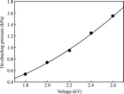
Abstract: Electrostatic chucks are one of the core components of semiconductor devices. As a key index of electrostatic chucks, the clamping force must be controlled within a reasonable range. Therefore, it is essential to accurately measure the clamping force. To reduce the negative factors influencing measurement precision and repeatability, this article presents a novel method to measure the clamping force and we elaborate both the principle and the key procedure. A micro-force probe component is introduced to monitor, adjust, and eliminate the gap between the wafer and the electrostatic chuck. The contact force between the ruby probe and the wafer is selected as an important parameter to characterize de-chucking, and we have found that the moment of de-chucking can be exactly judged. Moreover, this article derives the formula calibrating equivalent action area of backside gas pressure under real working conditions, which can effectively connect the backside gas pressure at the moment of de-chucking and the clamping force. The experiments were then performed on a self-designed measuring platform. The de-chucking mechanism is discussed in light of our analysis of the experimental data. Determination criteria for de-chucking point are summed up. It is found that the relationship between de-chucking pressure and applied voltage conforms well to quadratic equation. Meanwhile, the result reveals that actual de-chucking behavior is much more complicated than the description given in the classical empirical formula.

Key words: electrostatic chuckwaferclamping forcede-chuckingmeasuring method

Electrostatic chucks are one of the most important components of many semiconductor devices and they have been widely used in various manufacturing processes,such as etching,ion implantation,physical vapor deposition (PVD),plasma enhanced chemical vapor deposition (PECVD),and extreme ultraviolet lithography (EUVL). The main principle of an electrostatic chuck is as follows. Direct current (DC) voltages are applied on electrostatic electrodes embedded in dielectric layer of electrostatic chuck,and electrostatic fields between electrodes and silicon wafer are generated. Induced electrostatic charges that have opposite polarities accumulate on the upper surface of the dielectric layer and the lower surface of the wafer. Thus,an electrostatic attractive force comes into being and its distribution is uniform. The wafer is firmly clamped and held on the dielectric layer of the electrostatic chuck. Moreover,an electrostatic chuck has some additional functions,including controlling the surface temperature of the wafer,restraining thermal deformation,ensuring the flatness of the wafer,and adjusting the energy and spattering direction of plasma in a process chamber,etc. The clamping force is the leading parameter and the most important technical indicator of electrostatic chuck because it can directly or indirectly influence other parameters,such as the value and distribution of wafer temperature,wafer flatness,and so on. This may influence the processing quality and production efficiency of the wafer. Accordingly,clamping force has become one of the principal objectives of optimization design for electrostatic chucks[1]. The clamping force must be within a reasonable range and too strong or too weak a clamping force will not be permitted. Thus,accurate measurement of clamping force is essential. However,the generation mechanism and elimination mechanism of the clamping force are very complicated and so far they have not been perfectly explained. It should be pointed out that theoretical models and numerical simulations cannot accurately calculate and predict the clamping force for an electrostatic chuck[2]. Consequently,scientists have to fall back on experimental means. Nevertheless,the clamping force belongs to the internal force between a wafer and an electrostatic chuck,so it is not easy to directly measure this kind of force. This has become one of the key technical problems in the semiconductor industry and it needs to be solved urgently.

Although there are some studies concerning the measurement of the clamping force for an electrostatic chuck,the measuring principles and methods are commonly simple and they lack a detailed description and further investigation. Several of the measuring principles and methods that have been used in previous studies will be described in the following subsections.

The mechanical pulling method is commonly used in some of the available studies published by Yamagata University[3, 4],Hitachi High-Technologies Corporation[5],TNO TPD[6] and Yonsei University[7],etc. This principle is very simple and direct. A driving device (such as a linear motor,electrical push rod,or air cylinder) vertically pulls the wafer that is clamped on the surface of an electrostatic chuck by a corresponding connector. The pulling force increases gradually to counterbalance the clamping force until de-chucking occurs. At the moment of de-chucking,the pulling force is measured by means of a force sensor. The pulling force is equivalent to the clamping force of the electrostatic chuck. However,this method has a remarkable flaw because of the non-uniform load of the wafer,which will lead to local de-chucking. Thus,the measured clamping force cannot be accurate.

In order to overcome the shortcomings of the mechanical pulling method,the National Taiwan University[8] and Nagoya University[9] put forward the backside gas pressure equilibrium method. The authors create a gas gap that has a controlled pressure via a backside gas channel on the electrostatic chuck. De-chucking will occur when the backside gas pressure on the wafer counterbalances the clamping force. De-chucking can be detected by various means. Because gas pressure is a distributed force,this method can produce a uniform load on the wafer. However,the research published by the National Taiwan University only qualitatively analyzes the clamping force for different wafers,and it lacks quantitative analysis and actual measurement. In addition,the research published by Japan Nagoya University neglects that the local gas gap might have increased before overall de-chucking occurs,which will lead to a decrease of the clamping force. Consequently,this may cause systematic errors to arise.

The deformation comparison method was presented by the Fraunhofer Institute[10] and by Berliner GlasKGaA[11]. The main measuring principle is as follows. The lower surface of an elaborate wafer has a characteristic pin array and the deflection of each pin is measured by a laser interferometer while chucking. The experimental data are then compared with the simulation results,and the relative value and distribution of the clamping force can be qualitatively determined. Obviously,this method is unsuitable to measure a definite value of clamping force and so its application is limited.

In summary,all of the existing measuring methods of the clamping force of an electrostatic chuck have a number of different flaws. In particular,most measuring methods must determine the moment of the entire de-chucking of the wafer. However,de-chucking of the wafer is usually a continuous process and it is very easy to cause a misjudgment. In other words,before the entire de-chucking of the wafer is detected,local de-chucking of the wafer might actually have occurred. Thus,the gap between the wafer and the electrostatic chuck has increased. There is a close relationship between clamping force and the gap[12]. The clamping force will decline sharply with a slight increase of the gap. As a result,the measured clamping force tends to be less than that under working conditions,which leads to systematic errors. In addition,the wafer is in a non-equilibrium state at the moment of entire de-chucking,which delays the measuring instrument response,and this will greatly increase the systematic errors. On the one hand,in order to eliminate dynamic loads as much as possible,the whole measuring process should be quasi-static. On the other hand,the gap must be determined rapidly and accurately to avoid the influence of local de-chucking. At the moment,because the gap has no obvious change,there is little deviation between the measured clamping force and the real clamping force. Therefore,the reduction of systematic errors needs advanced measuring means and high detection sensitivity. Meanwhile,it is necessary to improve the criteria of de-chucking and select appropriate parameters that characterize de-chucking.

In light of the above analysis,this article puts forward a novel measuring method of the clamping force and it gives the key measuring steps for an electrostatic chuck on the basis of the backside gas pressure equilibrium method,which has the advantages of accuracy and reliability. A complete measuring platform is devised and built to carry out the experiments. We have been able to obtain a lot of valid experimental data and correlation curves,and the characteristics of the curves will be concluded and explained. We will then investigate the mechanism of corresponding de-chucking process and discuss how to judge the moment of de-chucking. Thus,the relationship between backside gas pressure at the moment of de-chucking and the voltage applied on the electrodes can be built. Furthermore,this article also proposes an effective way to connect the backside gas pressure at the moment of de-chucking and the clamping force of the electrostatic chuck.

As shown in Figure 1,a micro-force probe component is introduced,including a precision linear feed mechanism,a micro-force sensor,and a ruby probe. After the wafer has been firmly clamped by an electrostatic chuck,a precision linear feed mechanism starts to slowly drive the micro-force sensor and ruby probe towards the wafer. The ruby probe slightly touches the upper surface of the wafer,which are perpendicular to each other. The contact force between the ruby probe and wafer is monitored by a micro-force sensor and when it is exceeds a set threshold value,the movement of precision linear feed mechanism should be stopped immediately in order to ensure that the contact force is far less than the clamping force. In fact,the contact force is determined by the threshold value,the stiffness of micro-force sensor,the feed rate,and the feed mechanism characteristics. Thus,the above mentioned goal can be fulfilled so long as the corresponding parameters are selected properly. We then consider that the contact force is approximately zero at this time.

1.  Schematic diagram of the new measuring method.

As the backside gas pressure is steadily raised,the support force between the wafer and electrostatic chuck will gradually decrease. At the moment of de-chucking,the support force provided by the electrostatic chuck disappears completely and the ruby probe begins to provide the support force for the wafer,which leads to a remarkable rise of the contact force between the ruby probe and the wafer. In other words,this means that de-chucking occurs and the relevant criteria are found. Accordingly,the contact force between the ruby probe and wafer can be regarded as the selected parameter characterizing de-chucking,and it can be accurately measured and displayed by a micro-force sensor. In addition,the gap between the wafer and electrostatic chuck may be calculated by the contact force and the stiffness of the micro-force sensor,and it has an upper limit,which can be effectively controlled by adjusting the corresponding parameters.

(1) After the wafer has been clamped firmly by the electrostatic chuck,the electronic control system is started and the precision linear feed mechanism drives the ruby probe to drop slowly,making it touch the wafer slightly. When the reading of the micro-force sensor increases suddenly,the movement of the precision linear feed mechanism should be stopped at once.

(2) The air supply system is opened,and the backside gas pressure rises smoothly and steadily. The contact force between the ruby probe and the wafer,and the backside gas pressure at each time are recorded simultaneously.

(3) De-chucking begins to be detected when the reading of the micro-force sensor suddenly increases again. The backside gas pressure still continues to be raised slowly and evenly.

(4) When the reading of the micro-force sensor reaches a certain percentage of its full scale,which can be set according to realistic measurement demands,the air supply will automatically be cut off and the measurement is finished.

(5) After the power source of electrostatic chuck is shut off,the two lead wires (respectively,corresponding to the anode and cathode of the electrostatic electrodes) should be short-circuited to eliminate residual charges,which allows us to avoid the effect of the residual electrostatic force and ensure the independence of each measurement.

(6) By processing and analyzing the original data from the measurements,we can determine the moment of de-chucking and the corresponding backside gas pressure,which will be described in detail for various types of de-chucking later in this article.

Because one of the actual measured parameters in this article is backside gas pressure,it must be converted into the resultant force acting on the backside,so that the clamping force for the electrostatic chuck can be obtained by establishing an equilibrium equation. However,as a bridge linking backside gas pressure and the resultant force acting on the backside,the action area of backside gas pressure is unknown. The existing methods usually believe that it equals the area of the wafer surface not contacting the pins on dielectric layer of electrostatic chuck; namely,subtracting the area of pins from the total area of wafer. But this hypothesis is too ideal and it can only be applied to strict conditions of very low gas flow rate and superb flatness of pins and wafer. In fact,the contact status of the pins and wafer backside is quite complicated and also varies with the gap. Under normal circumstances,we cannot directly draw the above conclusion. The area is usually unavailable in theoretical analysis and numerical simulation. Hence,it is necessary to rely on experimental means. This article presents a wafer weight equilibrium method to calculate and calibrate the equivalent action area of the backside gas pressure under real working conditions.

When a wafer is normally placed on an electrostatic chuck,the force diagram of the wafer at the moment of de-chucking is shown in Figure 2(a). After the whole system is turned upside down,the force diagram of wafer at the moment of de-chucking is shown in Figure 2(b). For the two cases,we use the new measuring method to perform the experiments with the same applied DC voltages and other conditions. The backside gas pressures at the moment of de-chucking under normal state and inversion state can then be obtained. By the way,random errors will be reduced by averaging the multiple experimental results.

2.  Schematic diagram of the calibration of the equivalent action area of the backside gas pressure. (a) Normal state. (b) Inversion state.

According to Figure 2(a),the force equilibrium equation of wafer is as follows:

(p0+pback,1)Aback=p0Aall+Gwafer+Felec.
(1)

According to Figure 2(b),the force equilibrium equation of wafer is as follows:

(p0+pback,2)Aback=p0AallGwafer+Felec.
(2)
Here,p0 is atmospheric pressure,and pback,1 and pback,2 are the backside gas pressures relative to atmospheric pressure at the moment of de-chucking under normal state and inversion state,respectively. Aback is the equivalent action area of the backside gas pressure and Aall is the total area of the wafer surface. Gwafer is the wafer weight and Felec is the total clamping force of the electrostatic chuck.

Equation (1) minus Equation (2) gives:

(pback,1pback,2)Aback=2Gwafer.
That is:
Aback=2Gwaferpback,1pback,2.
(3)

Equation (3) is the formula calibrating the equivalent action area of the backside gas pressure under real working conditions. Thus,we can easily calculate the clamping force of the electrostatic chuck.

Equation (3) is plugged into Equation (1),and the final result is as follows:

Felec=2p0+pback,1+pback,2pback,1pback,2Gwaferp0Aall.
(4)

In our experiments,the wafer is made of monocrystalline silicon,with a diameter of 300 mm and a thickness of 1 mm. As is shown in Figure 3,the electrostatic chuck belongs to the bipolar Coulomb type and two interdigitated spiral tungsten electrodes are embedded in an aluminum oxide ceramic dielectric layer. Many round pins are uniformly distributed on the upper surface of the dielectric layer. DC power source is connected to the electrodes by means of a standard joint,providing the required high voltages.

3.  The electrostatic chuck used in the experiments.

The self-designed experimental platform is shown in Figure 4. It consists of a micro-force probe component,a backside gas pressure control system,a mechanical structure,and a measuring control and data acquisition system. The role of the micro-force probe component has been described in the previous section. Here,the micro-force sensor is a LSB200,made by FUTEK Co.,USA,with a full scale of 0.1 N and a resolution of 0.05% FS. The photoelectric actuator that is selected as the precision linear feed mechanism is a LAC10A-T4,made by ZABER Co.,Canada,with a travel distance of 10 mm and a repeated positioning accuracy of 1.5 μm. The probe includes a tungsten carbide rod with high rigidity and a ruby ball with a diameter of 1.5 mm,made by ZEISS Co.,Germany. The backside gas pressure control system supplies stable and controllable gas through the backside gas channel of the electrostatic chuck,and it is used to measure the real-time gas pressure at the entrance of the channel. Compressed gas from an air pump successively passes through the electromagnetism directional valve,mechanical pressure reducing valve,and electronic proportional valve,entering the channel entrance and gas pressure sensor,respectively. All of the applied valves were produced by SMC Co.,Japan. The gas pressure sensor is a STD720,made by Honeywell Co.,USA,with an accuracy of 0.07% FS. These pneumatic elements are connected by flexible pipes and a standard pneumatic quick release coupling. The function of the mechanical structure is to position and support all of the other components. The mechanical structure includes the bearing plate of the electrostatic chuck,the connecting plate of the micro-force probe component,and the framework,which are assembled by standard slotted section bars that are made of aluminum alloy to reduce weight and keep the structure firm. The purpose of the measuring control and data acquisition system is to automatically control the whole measuring process,to acquire the data of each sensor,and to transmit the data to a personal computer (PC) for storage. The core device of the system is a micro controller unit (MCU). The various interface circuits matching with micro-force probe component and backside gas pressure control system are also designed and constructed. The tests prove that the system can obtain a great deal of valid data within a short period of time and greatly improve the measuring efficiency.

4.  Experimental platform.

The experiments are performed under ambient conditions in our laboratory room. We alter the voltage applied on the electrodes and repeat the experiments. The data of the contact force between the ruby probe and the wafer,and the backside gas pressure under different voltages can be read simultaneously by a micro-force sensor and gas pressure sensor. Our preliminary experiments show that when the applied voltage is less than 1.6~kV,the clamping force is so small that local de-chucking of the wafer will occur as soon as the air supply system is opened. On the other hand,the rated operational voltage of the electrostatic chuck is 3 kV. Therefore,in formal experiments,the applied voltage varies from 1.8 to 2.6 kV,with an interval of 0.2 kV. It is worth noting that eight groups of valid data under each voltage are obtained by repeated measurements; i.e.,the total number of groups of obtained experimental data is 40.

The recorded original data in the experiments are contact force (F) and backside gas pressure (p),which change with time (t). In order to clearly observe the key turning points,we convert the original data to an F--p curve by eliminating time. The vertical axis represents the contact force between the ruby probe and wafer,and the horizontal axis represents the backside gas pressure

As is shown in Figure 5,a typical curve usually includes two parts. In the left part,the contact force has little change with backside gas pressure,while in the right part the contact force rises sharply. There is an obvious turning point between the two parts. In addition,although other turning points may exist in the curve,they have little effect on the overall trend of the curve and can be negligible. This type of curve fully conforms to theoretical analysis and prediction. Experimental results indicate that it accounts for the vast majority of all of the obtained curves.

5.  Typical relationship between contact force and backside gas pressure.

For the right part of the curve,a small growth of backside gas pressure will cause a great increase of the contact force. The main reason for this is that local de-chucking at the contact point of the ruby probe and wafer has occurred,leading to an instable equilibrium between the resultant force of the backside gas and the clamping force of the electrostatic chuck. This gap will enlarge little by little with a gradual decrease of the clamping force,which can bring about a further decrease of the clamping force. Due to the high stiffness of the wafer and the existence of a clamping force at the rest of wafer,entire de-chucking has not finished. If the backside gas pressure continues to be raised,the contact force between the ruby probe and the wafer will begin to grow rapidly to counteract the resultant force of the backside gas beyond the clamping force,so that the contact force will rise sharply with the steady growth of the backside gas pressure.

As shown in Figure 6,the overall trend of this type of curve is different from that of typical curves. At first,the contact force rises as backside gas pressure increases. When it reaches the peak,the trend of the curve changes suddenly and the contact force drops rapidly as backside gas pressure increases. It should be noted that such curves only account for a very small proportion of all of the obtained curves.

6.  Non-typical relationship between contact force and backside gas pressure.

Apparently,at first the whole wafer is still in a stable clamping state. After the contact force reaches the peak,the local gap between wafer center and electrostatic chuck narrows and the clamping force becomes stronger. Thereafter,the contact force begins to decline slowly. Consequently,there is a fast transition from one physical mode to another at the peak of the contact force. For the former,the gap between wafer center and electrostatic chuck is larger,whereas the gap between the wafer periphery and the electrostatic chuck is smaller,and a stable clamping effect can be maintained as a whole. For the latter,the gap between the wafer center and the electrostatic chuck is smaller and the local clamping effect is strong,yet the gap between the wafer periphery and electrostatic chuck is larger,resulting in periphery de-chucking. Moreover,because the tiny holes connected to the backside gas channel are close to the periphery of the electrostatic chuck,periphery de-chucking may destroy the contact seal and then cause a greatly enhanced flow.

From the major characteristics of the obtained curves and corresponding de-chucking mechanism,we can conclude the general criteria determining the de-chucking point. The characteristics described in typical and non-typical curves all mark large-area instability de-chucking of the wafer,so the key turning points should be regarded as de-chucking points. For typical curves,the de-chucking point refers to the only turning point. For non-typical curves,the peak of the contact force is selected as a de-chucking point.

According to the above principle,de-chucking points and corresponding backside gas pressure are identified and determined from all of the obtained curves. Thus,the correlation between backside gas pressure at the moment of de-chucking and the voltage applied on the electrodes can be established,and the box plots are shown in Figure 7.

7.  Box plots of backside gas pressure at the moment of dechucking with the change of applied voltage.

The median of de-chucking pressure under same voltage is adopted and a curve is fitted using a quadratic polynomial. The fitting result is shown in Figure 8,and the equation is as follows:

p=0.4935U20.9019U+0.5609.
(5)
Here,p denotes the value of backside gas pressure at the moment of de-chucking,and U denotes the value of applied voltage.

8.  Fitting curve of experimental data.

The fitting correlation coefficient is 0.9953.

The high fitting correlation coefficient suggests that the experimental data accord well with the fitting polynomial,verifying the rationality and feasibility of the novel method of measuring the clamping force that has been developed in this article. In the empirical formula of the clamping force for the Coulomb type electrostatic chuck,the clamping force is proportional to the square of the voltage[13]. For the fitting equation,the constant term results from the wafer weight and the atmospheric pressure. There are several explanations for the source of the linear term. On the one hand,the dependent variable of the fitting function is the backside gas pressure at the moment of de-chucking,while the dependent variable of the empirical formula refers to the clamping force. As a bridge connecting the two parameters,the equivalent action area of backside gas pressure might not be a constant and it should be relevant to the applied voltage. The calibration method presented in this article is applicable to constant voltage. If the voltage changes,then the calibration needs to be performed anew. On the other hand,the result also reveals the high complexity of the generation of the clamping force and de-chucking mechanism. However,unknown factors influencing the clamping force remain to be found,which need to be further studied.

There are several factors influencing the measurement precision and repeatability in existing measuring methods of clamping force for electrostatic chucks,including the deformation of the wafer,the enlargement of the gap between wafer and electrostatic chuck,and so on. To overcome these shortcomings,this article presents a new idea based on the previous backside gas pressure equilibrium method,and demonstrates the measuring principle and key procedure. A micro-force probe component is introduced to monitor,adjust,and eliminate the gap between the wafer and the electrostatic chuck. The contact force between the ruby probe and the wafer is selected as the parameter to characterize de-chucking,and the moment of de-chucking can be exactly judged. Our method ensures that the whole system is in a quasi-static state,which allows us to avoid the systematic errors resulting from transient process and improve the measurement precision. Meanwhile,it has a high sensitivity and can quickly and accurately detect de-chucking before the gap increases,reducing the effect of local de-chucking and decreasing the measurement errors. Moreover,this article puts forward a wafer weight equilibrium method to calculate and calibrate the equivalent action area of the backside gas pressure under real working conditions,thereby building a bridge between the measured parameter and objective parameter.

Formal experiments were then carried out by means of a self-designed measuring platform. After processing the experimental data,we have obtained many groups of the curve between the contact force of the ruby probe and the backside gas pressure. These curves are divided into two types,consisting of typical and non-typical curves. Their basic characteristics are described and the corresponding de-chucking mechanism is discussed. The general criteria are concluded,which can be used to determine the de-chucking point. We then used them to establish the correlation between the backside gas pressure at the moment of de-chucking and the applied voltage,and we performed the fitting of the experimental data with a quadratic polynomial. The result demonstrates the novel measuring method of clamping force proposed in this article is reasonable and feasible. At the same time,this work shows that actual de-chucking behavior is much more complicated than the description given in the classical empirical formula,which deserves further research.


[1]
[2]
[3]
[4]
[5]
[6]
[7]
[8]
[9]
[10]
[11]
[12]
[13]
Fig. 1.  Schematic diagram of the new measuring method.

Fig. 2.  Schematic diagram of the calibration of the equivalent action area of the backside gas pressure. (a) Normal state. (b) Inversion state.

Fig. 3.  The electrostatic chuck used in the experiments.

Fig. 4.  Experimental platform.

Fig. 5.  Typical relationship between contact force and backside gas pressure.

Fig. 6.  Non-typical relationship between contact force and backside gas pressure.

Fig. 7.  Box plots of backside gas pressure at the moment of dechucking with the change of applied voltage.

Fig. 8.  Fitting curve of experimental data.

DownLoad: CSV
DownLoad: CSV
DownLoad: CSV
DownLoad: CSV
DownLoad: CSV
DownLoad: CSV
[1]
[2]
[3]
[4]
[5]
[6]
[7]
[8]
[9]
[10]
[11]
[12]
[13]
1

A 130-nm ferroelectric nonvolatile system-on-chip for internet of things

Zhiyi Yu

Journal of Semiconductors, 2019, 40(2): 020205. doi: 10.1088/1674-4926/40/2/020205

2

Contact etch process optimization for RF process wafer edge yield improvement

Zhangli Liu, Bingkui He, Fei Meng, Qiang Bao, Yuhong Sun, et al.

Journal of Semiconductors, 2019, 40(12): 122402. doi: 10.1088/1674-4926/40/12/122402

3

Interfacial engineering of printable bottom back metal electrodes for full-solution processed flexible organic solar cells

Hongyu Zhen, Kan Li, Yaokang Zhang, Lina Chen, Liyong Niu, et al.

Journal of Semiconductors, 2018, 39(1): 014002. doi: 10.1088/1674-4926/39/1/014002

4

Engineering in-plane silicon nanowire springs for highly stretchable electronics

Zhaoguo Xue, Taige Dong, Zhimin Zhu, Yaolong Zhao, Ying Sun, et al.

Journal of Semiconductors, 2018, 39(1): 011001. doi: 10.1088/1674-4926/39/1/011001

5

Impact of underlap spacer region variation on electrostatic and analog performance of symmetrical high-k SOI FinFET at 20 nm channel length

Neeraj Jain, Balwinder Raj

Journal of Semiconductors, 2017, 38(12): 122002. doi: 10.1088/1674-4926/38/12/122002

6

Method to remove wafer surface particles

Bo Peng, Deguang Zheng, Yue Yu

Journal of Semiconductors, 2017, 38(9): 096004. doi: 10.1088/1674-4926/38/9/096004

7

Design space of electrostatic chuck in etching chamber

Yuchun Sun, Jia Cheng, Yijia Lu, Yuemin Hou, Linhong Ji, et al.

Journal of Semiconductors, 2015, 36(8): 084004. doi: 10.1088/1674-4926/36/8/084004

8

Finite element analysis on factors influencing the clamping force in an electrostatic chuck

Xingkuo Wang, Jia Cheng, Kesheng Wang, Yiyong Yang, Yuchun Sun, et al.

Journal of Semiconductors, 2014, 35(9): 094011. doi: 10.1088/1674-4926/35/9/094011

9

A novel high performance ESD power clamp circuit with a small area

Yang Zhaonian, Liu Hongxia, Li Li, Zhuo Qingqing

Journal of Semiconductors, 2012, 33(9): 095006. doi: 10.1088/1674-4926/33/9/095006

10

Improved light extraction of wafer-bonded AlGaInP LEDs by surface roughening

Liu Zike, Gao Wei, Xu Chen, Zou Desu, Qin Yuan, et al.

Journal of Semiconductors, 2010, 31(11): 114011. doi: 10.1088/1674-4926/31/11/114011

11

A new cleaning process combining non-ionic surfactant with diamond film electrochemical oxidation for polished silicon wafers

Gao Baohong, Zhu Yadong, Liu Yuling, Wang Shengli, Zhou Qiang, et al.

Journal of Semiconductors, 2010, 31(7): 076002. doi: 10.1088/1674-4926/31/7/076002

12

Structural and electrical characteristics of lanthanum oxide gate dielectric film on GaAs pHEMT technology

Wu Chia-Song, Liu Hsing-Chung

Journal of Semiconductors, 2009, 30(11): 114004. doi: 10.1088/1674-4926/30/11/114004

13

Wafer level hermetic packaging based on Cu–Sn isothermal solidification technology

Cao Yuhan, Luo Le

Journal of Semiconductors, 2009, 30(8): 086001. doi: 10.1088/1674-4926/30/8/086001

14

A wafer-level 3D packaging structure with Benzocyclobutene as a dielectric for multichip module fabrication

Geng Fei, Ding Xiaoyun, Xu Gaowei, Luo Le

Journal of Semiconductors, 2009, 30(10): 106003. doi: 10.1088/1674-4926/30/10/106003

15

Influence of Polarization-Induced Electric Fields on Optical Properties of Intersubband Transitions in AlxGa1-xN/GaN Double Quantum Wells

Lei Shuangying, Shen Bo, Xu Fujun, Yang Zhijian, Xu Ke, et al.

Chinese Journal of Semiconductors , 2006, 27(3): 403-408.

16

Analysis of PTCDA/ITO Surface and Interface Using X-ray Photoelectron Spectroscopy and Atomic Force Microscopy

Tang Ning, Shen Bo, Wang Maojun, Yang Zhijian, Xu Ke, et al.

Chinese Journal of Semiconductors , 2006, 27(2): 235-238.

17

Analysis of PTCDA/ITO Surface and Interface Using X-ray Photoelectron Spectroscopy and Atomic Force Microscopy

Ou Guping, Song Zhen, Gui Wenming, Zhang Fujia

Chinese Journal of Semiconductors , 2006, 27(2): 229-234.

18

An Improved Angle Polishing Method for Measuring Subsurface Damage in Silicon Wafers

Huo Fengwei, Kang Renke, Guo Dongming, Zhao Fuling, Jin Zhuji, et al.

Chinese Journal of Semiconductors , 2006, 27(3): 506-510.

19

A New Method to Retrieve Proximity Effect Parameters in Electron-Beam Lithography

Kang Xiaohui, Li Zhigang, Liu Ming, Xie Changqing, and Chen Baoqin, et al.

Chinese Journal of Semiconductors , 2005, 26(3): 455-459.

20

A Wavelength Tunable DBR Laser Integrated with an Electro-Absorption Modulator by a Combined Method of SAG and QWI

Zhang Jing, Li Baoxia, Zhao Lingjuan, Wang Baojun, Zhou Fan, et al.

Chinese Journal of Semiconductors , 2005, 26(11): 2053-2057.

1. Sun, S., Zhao, J. The Influence of Electrode Structure and Wafer Material on Chuck Force of Coulomb Electrostatic Chuck | [库仑型静电卡盘吸附力受电极结构及晶圆氧化层影响的研究]. Zhenkong Kexue yu Jishu Xuebao/Journal of Vacuum Science and Technology, 2023, 43(8): 681-688. doi:10.13922/j.cnki.cjvst.202302012
2. Sun, S., Zhao, J. Influence of Wafer Material on Chuck Force of J-R Type Electrostatic Chuck | [晶圆材料对 J-R 型静电卡盘吸附力影响的研究]. Zhenkong Kexue yu Jishu Xuebao/Journal of Vacuum Science and Technology, 2023, 43(6): 554-562. doi:10.13922/j.cnki.cjvst.202211018
3. Sun, S., Zhao, J. The Effect of Structure and Electrical Properties of the Mesa on the Electrostatic Chuck Force | [凸点结构及电学性能对 J-R 型静电卡盘吸附力影响的研究]. Zhenkong Kexue yu Jishu Xuebao/Journal of Vacuum Science and Technology, 2023, 43(4): 305-313. doi:10.13922/j.cnki.cjvst.202207010
4. Wang, K., Lu, Y., Cheng, J. et al. Prediction of residual clamping force for Coulomb type and Johnsen–Rahbek type of bipolar electrostatic chucks. Proceedings of the Institution of Mechanical Engineers, Part C: Journal of Mechanical Engineering Science, 2019, 233(1): 302-312. doi:10.1177/0954406218756938
  • Search

    Advanced Search >>

    GET CITATION

    Kesheng Wang, Jia Cheng, Yin Zhong, Linhong Ji. A novel measuring method of clamping force for electrostatic chuck in semiconductor devices[J]. Journal of Semiconductors, 2016, 37(4): 044012. doi: 10.1088/1674-4926/37/4/044012
    K S Wang, J Cheng, Y Zhong, L H Ji. A novel measuring method of clamping force for electrostatic chuck in semiconductor devices[J]. J. Semicond., 2016, 37(4): 044012. doi: 10.1088/1674-4926/37/4/044012.
    shu

    Export: BibTex EndNote

    Article Metrics

    Article views: 5882 Times PDF downloads: 299 Times Cited by: 4 Times

    History

    Received: 25 November 2015 Revised: Online: Published: 01 April 2016

    Catalog

      Email This Article

      User name:
      Email:*请输入正确邮箱
      Code:*验证码错误
      Kesheng Wang, Jia Cheng, Yin Zhong, Linhong Ji. A novel measuring method of clamping force for electrostatic chuck in semiconductor devices[J]. Journal of Semiconductors, 2016, 37(4): 044012. doi: 10.1088/1674-4926/37/4/044012 ****K S Wang, J Cheng, Y Zhong, L H Ji. A novel measuring method of clamping force for electrostatic chuck in semiconductor devices[J]. J. Semicond., 2016, 37(4): 044012. doi: 10.1088/1674-4926/37/4/044012.
      Citation:
      Kesheng Wang, Jia Cheng, Yin Zhong, Linhong Ji. A novel measuring method of clamping force for electrostatic chuck in semiconductor devices[J]. Journal of Semiconductors, 2016, 37(4): 044012. doi: 10.1088/1674-4926/37/4/044012 ****
      K S Wang, J Cheng, Y Zhong, L H Ji. A novel measuring method of clamping force for electrostatic chuck in semiconductor devices[J]. J. Semicond., 2016, 37(4): 044012. doi: 10.1088/1674-4926/37/4/044012.

      A novel measuring method of clamping force for electrostatic chuck in semiconductor devices

      DOI: 10.1088/1674-4926/37/4/044012
      Funds:

      Project supported by No. 02 National Science and Technology Major Project of China (No. 2011ZX02403-004).

      More Information
      • Corresponding author: Wang Kesheng,Email:wks11@mails.tsinghua.edu.cn
      • Received Date: 2015-11-25
      • Accepted Date: 2015-12-22
      • Published Date: 2016-01-25

      Catalog

        /

        DownLoad:  Full-Size Img  PowerPoint
        Return
        Return