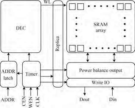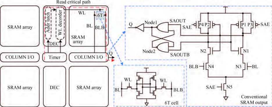
Fig. 1.
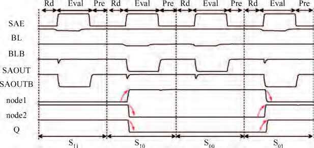
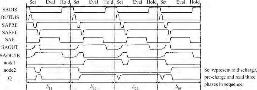
Analysis of SRAM read operation.
SEMICONDUCTOR INTEGRATED CIRCUITS
Keji Zhou1, Pengjun Wang1, and Liang Wen2
Corresponding author: Wang Pengjun,Email:wangpengjun@nbu.edu.cn
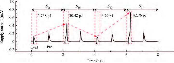
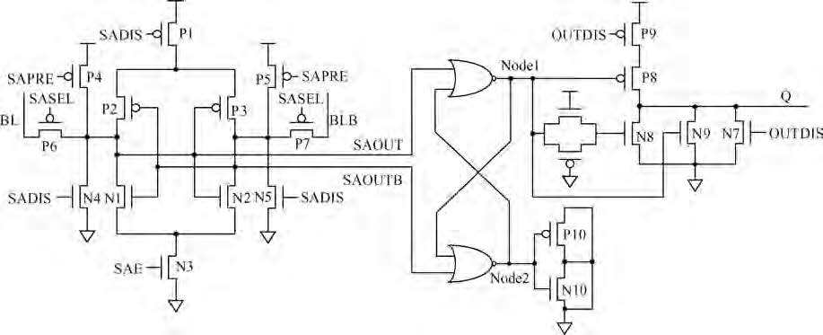
Abstract: A power balance static random-access memory (SRAM) for resistance to differential power analysis (DPA) is proposed. In the proposed design, the switch power consumption and short-circuit power consumption are balanced by discharging and pre-charging the key nodes of the output circuit and adding an additional short-circuit current path. Thus, the power consumption is constant in every read cycle. As a result, the DPA-resistant ability of the SRAM is improved. In 65 nm CMOS technology, the power balance SRAM is fully custom designed with a layout area of 5863.6 μm2.The post-simulation results show that the normalized energy deviation (NED) and normalized standard deviation (NSD) are 0.099% and 0.04%, respectively. Compared to existing power balance circuits, the power balance ability of the proposed SRAM has improved 53%.
Keywords: differential power analysis (DPA), static random access memory (SRAM), power balance, information security
| [1] | |
| [2] | |
| [3] | |
| [4] | |
| [5] | |
| [6] | |
| [7] | |
| [8] | |
| [9] | |
| [10] | |
| [11] | |
| [12] | |
| [13] | |
| [14] | |
| [15] |
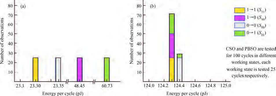
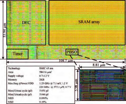
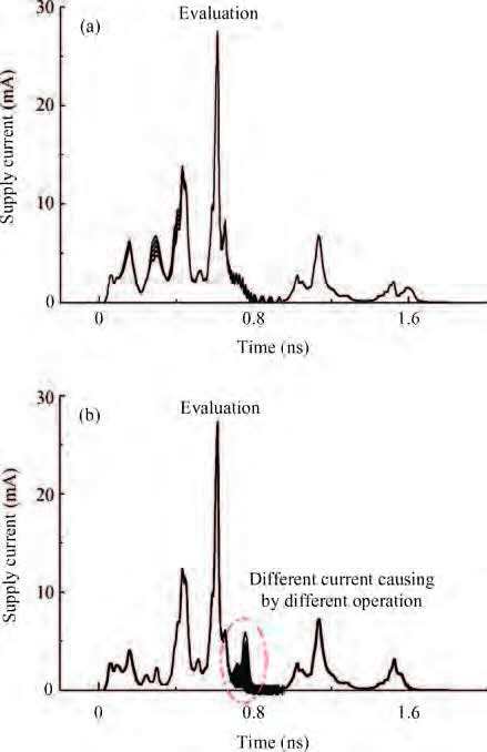
Table 2. Performances of power balance SRAM for DPA-resistance in different voltages and process corners.
 DownLoad: CSV
| [1] | |
| [2] | |
| [3] | |
| [4] | |
| [5] | |
| [6] | |
| [7] | |
| [8] | |
| [9] | |
| [10] | |
| [11] | |
| [12] | |
| [13] | |
| [14] | |
| [15] |


Article views: 3318 Times PDF downloads: 25 Times Cited by: 0 Times
Received: 19 August 2015 Revised: Online: Published: 01 April 2016
| Citation: |
Keji Zhou, Pengjun Wang, Liang Wen. Design of power balance SRAM for DPA-resistance[J]. Journal of Semiconductors, 2016, 37(4): 045002. doi: 10.1088/1674-4926/37/4/045002
****
K J Zhou, P J Wang, L Wen. Design of power balance SRAM for DPA-resistance[J]. J. Semicond., 2016, 37(4): 045002. doi: 10.1088/1674-4926/37/4/045002.

|
| [1] | |
| [2] | |
| [3] | |
| [4] | |
| [5] | |
| [6] | |
| [7] | |
| [8] | |
| [9] | |
| [10] | |
| [11] | |
| [12] | |
| [13] | |
| [14] | |
| [15] |

 WeChat ID
Journal of Semiconductors © 2017 All Rights Reserved 京ICP备05085259号-2