Fig. 1.
Typical $C$-$V$ curves of the three samples measured at a frequency of 1 MHz. Area of capacitor is 7.85 × 10⁻⁵ cm2.
SEMICONDUCTOR DEVICES
Wenyu Yuan, Jingping Xu, Lu Liu, Yong Huang and Zhixiang Cheng
Corresponding author: Jingping Xu, jpxu@hust.edu.cn
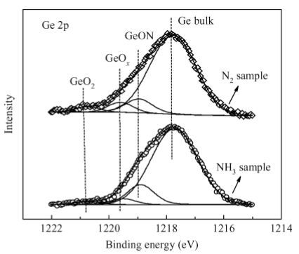
Abstract: The interfacial and electrical characteristics of Ge metal-oxide-semiconductor (MOS) devices with a dual passivation layer of ZrON/GeON formed by NH3- or N2-plasma treatment are investigated. The experimental results show that the NH3-plasma treated sample exhibits significantly improved interfacial and electrical properties as compared to the samples with N2-plasma treatment and no treatment: a lower interface-state density at the midgap (1.64 × 1011 cm-2·eV-1) and gate leakage current (9.32 × 10⁻⁵ A/cm2 at Vfb+ 1 V), a small capacitance equivalent thickness (1.11 nm) and a high k value (32). X-ray photoelectron spectroscopy is used to analyze the involved mechanisms. It is indicated that more GeON and less GeOx (x <2) are formed on the Ge surface during NH3-plasma treatment than the N2-plasma treatment, resulting in a high-quality high-k/Ge interface, because H atoms and NH radicals in NH3-plasma can enhance volatilization of the unstable low-k GeOx, creating high-quality GeON passivation layer. Moreover, more nitrogen incorporation in ZrON/GeON induced by NH3-plasma treatment can build a stronger N barrier and thus more effectively inhibit in-diffusion of O and Ti from high-k gate dielectric and out-diffusion of Ge.
Keywords: Ge MOS, NH3 plasma, interface properties, ZrON/GeON dual passivation layer
| [1] | |
| [2] | |
| [3] | |
| [4] | |
| [5] | |
| [6] | |
| [7] | |
| [8] | |
| [9] | |
| [10] | |
| [11] | |
| [12] | |
| [13] | |
| [14] | |
| [15] | |
| [16] | |
| [17] | |
| [18] | |
| [19] | |
| [20] | |
| [21] |
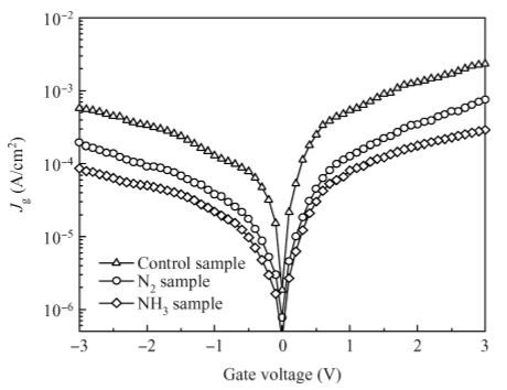
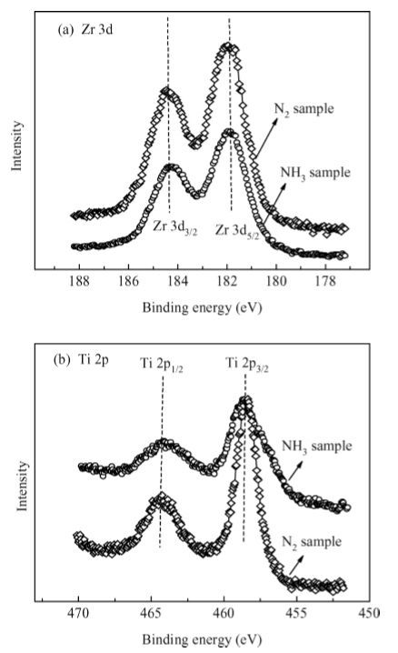
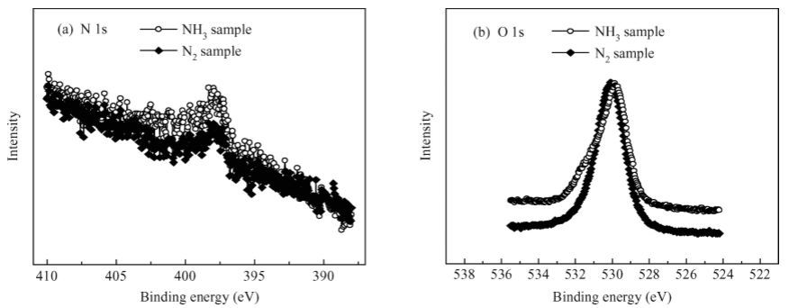
Table 1. Electrical and physical parameters of Ge MOS devices extracted from HF $C$-$V$ curves.
 DownLoad: CSV
| [1] | |
| [2] | |
| [3] | |
| [4] | |
| [5] | |
| [6] | |
| [7] | |
| [8] | |
| [9] | |
| [10] | |
| [11] | |
| [12] | |
| [13] | |
| [14] | |
| [15] | |
| [16] | |
| [17] | |
| [18] | |
| [19] | |
| [20] | |
| [21] |


Article views: 3229 Times PDF downloads: 25 Times Cited by: 0 Times
Received: 22 August 2015 Revised: Online: Published: 01 May 2016
| Citation: |
Wenyu Yuan, Jingping Xu, Lu Liu, Yong Huang, Zhixiang Cheng. Improved interfacial and electrical properties of Ge MOS devices with ZrON/GeON dual passivation layer[J]. Journal of Semiconductors, 2016, 37(5): 054004. doi: 10.1088/1674-4926/37/5/054004
****
W Y Yuan, J P Xu, L Liu, Y Huang, Z X Cheng. Improved interfacial and electrical properties of Ge MOS devices with ZrON/GeON dual passivation layer[J]. J. Semicond., 2016, 37(5): 054004. doi: 10.1088/1674-4926/37/5/054004.

|
| [1] | |
| [2] | |
| [3] | |
| [4] | |
| [5] | |
| [6] | |
| [7] | |
| [8] | |
| [9] | |
| [10] | |
| [11] | |
| [12] | |
| [13] | |
| [14] | |
| [15] | |
| [16] | |
| [17] | |
| [18] | |
| [19] | |
| [20] | |
| [21] |

 WeChat ID
Journal of Semiconductors © 2017 All Rights Reserved 京ICP备05085259号-2