


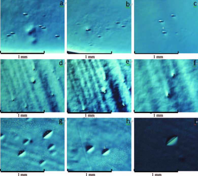
Fig. 1.
(Color online) Micrographs from two samples and reference wafer after preferential etching, (a)-(c) are belong to sample A, (d)-(f) for reference wafer, (g)-(I) for sample B.
SEMICONDUCTOR MATERIALS
Kewei Cao, Tong Liu, Jingming Liu, Hui Xie, Dongyan Tao, Youwen Zhao, Zhiyuan Dong and Feng Hui
Corresponding author: Kewei Cao, Email: caokewei@semi.ac.cn
Abstract: Low dislocation density Ge wafers grown by a vertical gradient freeze (VGF) method used for the fabrication of multi-junction photovoltaic cells (MJC) have been studied by a whole wafer scale measurement of the lattice parameter, X-ray rocking curves, etch pit density (EPD), impurities concentration, minority carrier lifetime and residual stress. Impurity content in the VGF-Ge wafers, including that of B, is quite low although B2O3 encapsulation is used in the growth process. An obvious difference exists across the whole wafer regarding the distribution of etch pit density, lattice parameter, full width at half maximum (FWHM) of the X-ray rocking curve and residual stress measured by Raman spectra. These are in contrast to a reference Ge substrate wafer grown by the Cz method. The influence of the VGF-Ge substrate on the performance of the MJC is analyzed and evaluated by a comparison of the statistical results of cell parameters.
Keywords: crystallities, X-ray diffraction, semiconducting germanium, semiconducting gallium arsenide, solar cells
| [1] |
Bett A W, Dimroth F, Stollwerck G, et al. Ⅲ-Ⅴ compounds for solar cell applications. Appl Phys A,1999, 69:119
|
| [2] |
Avrutin V, Izyumskaya N, Morkoç H, et al. Semiconductor solar cells:recent progress in terrestrial applications. Superlattices Microstruc, 2011, 49:337
|
| [3] |
Law D D, King R R, Yoon H, et al. Future technology pathways of terrestrial Ⅲ-Ⅴ multijunction solar cells for concentrator photovoltaic systems. Sol Energy Mater Sol Cells, 2010, 94:1314
|
| [4] |
Aiken D, Dons E, Je S S, et al. Lattice-matched solar cells with 40% average efficiency in pilot production and a roadmap to 50%. IEEE J Photovolt, 2013, 3:1
|
| [5] |
Luque A. Will we exceed 50% efficiency in photovoltaics. J Appl Phys, 2011, 110:031301
|
| [6] |
Green M A, Emery K, Hishikawa Y, et al. Solar cell efficiency tables (version 40). Prog Photovolt, 2012, 20:606
|
| [7] |
Fetzer C M,Yoon H, King R R, et al. 1.6/1.1 eV metamorphic GaInP/GaInAs solar cells grown by MOVPE on Ge. J Cryst Growth, 2005, 276:48
|
| [8] |
Liu X Q, Fetzer C M, Rehder E, et al. Organometallic vapor phase epitaxy growth of upright metamorphic multijunction solar cells. J Cryst Growth, 2012, 352:186
|
| [9] |
Surek T. Crystal growth and materials research in photovoltaics:progress and challenges. J Cryst Growth, 2004, 10:93
|
| [10] |
Taishi T, Ise H, Murao Y, et al. Oxygen doped Ge crystals Czochralski-grown from the B2O3-fully-covered melt. Microelectron Eng, 2011, 88:496
|
| [11] |
Taishi T, Ise H, Murao Y, et al. Czochralski-growth of germanium crystals containing high concentrations of oxygen impurities. J Cryst Growth, 2010, 312:2783
|
| [12] |
Frank-Rotsch CH, Rudolph P. Vertical gradient freeze of 4 inch Ge crystals in a heater-magnet module. J Cryst Growth, 2009, 311:2294
|
| [13] |
Langheinrich D, Pätzold O, Raabe L, et al. VGF growth of germanium single crystals without crucible contact. J Cryst Growth, 2010, 312:2291
|
| [14] |
Qu Xiaosheng, Zhang Sisi, Bao Hongyin, et al. The effect of InAs quantum-dot size and interdot distance on GaInP/GaAs/GaInAs/Ge multi-junction tandem solar cells. Journal of Semiconductors, 2013, 34(6):062003
|
| [15] |
Bellmann M P, Pätzold O, Stelter M, et al. Optimisation of the VGF growth process by inverse modelling. J Cryst Growth, 2010, 312:2175
|
| [16] |
Ignacio R S, Enrique B, Beatriz G, et al. Analysis of germanium epiready wafers for Ⅲ-Ⅴ heteroepitaxy. J Cryst Growth, 2008, 310:4803
|
| [17] |
Jin Chaohua. Numerical study of heat transport and fluid flow during the silicon crystal growth process by the Czochralski method. Journal of Semiconductors, 2013, 34(6):063005
|
| [18] |
Cooper A S. Precise lattice constants of germanium, aluminium, gallium arsenide, uranium, sulphur, quartz and sapphire. Acta Cryst, 1962, 15:578
|
| [19] |
Pinto S R C, Rolo A G, Chahboun A, et al. Raman study of stress effect on Ge nanocrystals embedded in Al2O3. Thin Solid Films, 2010, 518:5378
|
| [20] |
Nishioka T, Shinoda Y, Ohmachi Y. Raman microprobe analysis of stress in Ge and GaAs/Ge on SiO2 coated Si substrates. J Appl Phys,1985, 57:276
|
| [21] |
Yamaguchi M. Fundamentals and R&D status of Ⅲ-Ⅴ compound solar cells and materials. Phys Status Solidi C, 2015, 6:489
|
| [22] |
Yamaguchi M, Amano C. Efficiency calculations of thin film GaAs solar cells on Si substrates. J Appl Phys, 1985, 58:3601
|
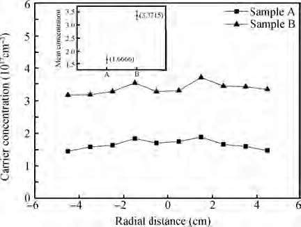
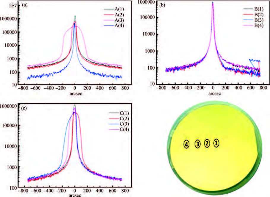
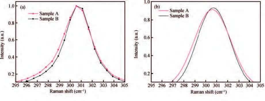
Table 1. Impurity content in Ge wafers (in ppm wt).
| B, Ag, V, Co, Cu | <0.005 | <0.005 |
| Ti, Cr, Ni, Pt | <0.01 | <0.01 |
| Mn, Mo, Fe | <0.5 | <0.5 |
| Au | <0.1 | <0.1 |
| Ga | 0.89 | 1.9 |
 DownLoad: CSV
Table 2. Bragg angle and lattice parameter.
| Sample | A | B |
| Bragg angle (°) | 33.018 | 33.013 |
| Lattice parameter (Å) | 5.6544 | 5.6551 |
DownLoad: CSV
Table 3. FWHM of two samples.
| Sample | A | B | |
| FWHM(arcsec) | 1 | 60.32 | 37.54 |
| 2 | 53.43 | 51.16 | |
| 3 | 202.8 | 94.47 | |
| 4 | 20.22 | 93.54 | |
DownLoad: CSV
Table 4. The peak shift, linewidth, calculated stress of three samples.
| Sample | A | B |
| Peak shift (cm-1) | 0.09 | 0.23 |
| Linewidth (cm-1) | 3.94 | 3.64 |
| Stress (109 dyne/cm2) | 0.306 | 0.782 |
DownLoad: CSV
Table 5. The performance of the MJC manufactured on each sample.
| Sample | A | B | Reference |
| Voc (mV) | 2525.4-2528.4 | 2629.4-2631.7 | 2633.4-2636.7 |
| Isc (mA) | 197.4-198.6 | 201.3-202.1 | 203.4-203.8 |
| Vmp (mV) | 2240.7-2248.5 | 2292.9-2293.3 | 2284.2-2284.3 |
| Imp (mA) | 188.4-191.8 | 194.2-196.1 | 197.2-198.7 |
| η (100%) | 26.01-26.56 | 27.44-27.69 | 27.74-27.96 |
| FF | 0.847-0.859 | 0.841-0.846 | 0.841-0.845 |
DownLoad: CSV
| [1] |
Bett A W, Dimroth F, Stollwerck G, et al. Ⅲ-Ⅴ compounds for solar cell applications. Appl Phys A,1999, 69:119
|
| [2] |
Avrutin V, Izyumskaya N, Morkoç H, et al. Semiconductor solar cells:recent progress in terrestrial applications. Superlattices Microstruc, 2011, 49:337
|
| [3] |
Law D D, King R R, Yoon H, et al. Future technology pathways of terrestrial Ⅲ-Ⅴ multijunction solar cells for concentrator photovoltaic systems. Sol Energy Mater Sol Cells, 2010, 94:1314
|
| [4] |
Aiken D, Dons E, Je S S, et al. Lattice-matched solar cells with 40% average efficiency in pilot production and a roadmap to 50%. IEEE J Photovolt, 2013, 3:1
|
| [5] |
Luque A. Will we exceed 50% efficiency in photovoltaics. J Appl Phys, 2011, 110:031301
|
| [6] |
Green M A, Emery K, Hishikawa Y, et al. Solar cell efficiency tables (version 40). Prog Photovolt, 2012, 20:606
|
| [7] |
Fetzer C M,Yoon H, King R R, et al. 1.6/1.1 eV metamorphic GaInP/GaInAs solar cells grown by MOVPE on Ge. J Cryst Growth, 2005, 276:48
|
| [8] |
Liu X Q, Fetzer C M, Rehder E, et al. Organometallic vapor phase epitaxy growth of upright metamorphic multijunction solar cells. J Cryst Growth, 2012, 352:186
|
| [9] |
Surek T. Crystal growth and materials research in photovoltaics:progress and challenges. J Cryst Growth, 2004, 10:93
|
| [10] |
Taishi T, Ise H, Murao Y, et al. Oxygen doped Ge crystals Czochralski-grown from the B2O3-fully-covered melt. Microelectron Eng, 2011, 88:496
|
| [11] |
Taishi T, Ise H, Murao Y, et al. Czochralski-growth of germanium crystals containing high concentrations of oxygen impurities. J Cryst Growth, 2010, 312:2783
|
| [12] |
Frank-Rotsch CH, Rudolph P. Vertical gradient freeze of 4 inch Ge crystals in a heater-magnet module. J Cryst Growth, 2009, 311:2294
|
| [13] |
Langheinrich D, Pätzold O, Raabe L, et al. VGF growth of germanium single crystals without crucible contact. J Cryst Growth, 2010, 312:2291
|
| [14] |
Qu Xiaosheng, Zhang Sisi, Bao Hongyin, et al. The effect of InAs quantum-dot size and interdot distance on GaInP/GaAs/GaInAs/Ge multi-junction tandem solar cells. Journal of Semiconductors, 2013, 34(6):062003
|
| [15] |
Bellmann M P, Pätzold O, Stelter M, et al. Optimisation of the VGF growth process by inverse modelling. J Cryst Growth, 2010, 312:2175
|
| [16] |
Ignacio R S, Enrique B, Beatriz G, et al. Analysis of germanium epiready wafers for Ⅲ-Ⅴ heteroepitaxy. J Cryst Growth, 2008, 310:4803
|
| [17] |
Jin Chaohua. Numerical study of heat transport and fluid flow during the silicon crystal growth process by the Czochralski method. Journal of Semiconductors, 2013, 34(6):063005
|
| [18] |
Cooper A S. Precise lattice constants of germanium, aluminium, gallium arsenide, uranium, sulphur, quartz and sapphire. Acta Cryst, 1962, 15:578
|
| [19] |
Pinto S R C, Rolo A G, Chahboun A, et al. Raman study of stress effect on Ge nanocrystals embedded in Al2O3. Thin Solid Films, 2010, 518:5378
|
| [20] |
Nishioka T, Shinoda Y, Ohmachi Y. Raman microprobe analysis of stress in Ge and GaAs/Ge on SiO2 coated Si substrates. J Appl Phys,1985, 57:276
|
| [21] |
Yamaguchi M. Fundamentals and R&D status of Ⅲ-Ⅴ compound solar cells and materials. Phys Status Solidi C, 2015, 6:489
|
| [22] |
Yamaguchi M, Amano C. Efficiency calculations of thin film GaAs solar cells on Si substrates. J Appl Phys, 1985, 58:3601
|


Article views: 4043 Times PDF downloads: 25 Times Cited by: 0 Times
Received: 15 October 2015 Revised: 10 November 2015 Online: Published: 01 June 2016
| Citation: |
Kewei Cao, Tong Liu, Jingming Liu, Hui Xie, Dongyan Tao, Youwen Zhao, Zhiyuan Dong, Feng Hui. Evaluation of four inch diameter VGF-Ge substrates used for manufacturing multi-junction solar cell[J]. Journal of Semiconductors, 2016, 37(6): 063002. doi: 10.1088/1674-4926/37/6/063002
****
K W Cao, T Liu, J M Liu, H Xie, D Y Tao, Y W Zhao, Z Y Dong, F Hui. Evaluation of four inch diameter VGF-Ge substrates used for manufacturing multi-junction solar cell[J]. J. Semicond., 2016, 37(6): 063002. doi: 10.1088/1674-4926/37/6/063002.

|
| [1] |
Bett A W, Dimroth F, Stollwerck G, et al. Ⅲ-Ⅴ compounds for solar cell applications. Appl Phys A,1999, 69:119
|
| [2] |
Avrutin V, Izyumskaya N, Morkoç H, et al. Semiconductor solar cells:recent progress in terrestrial applications. Superlattices Microstruc, 2011, 49:337
|
| [3] |
Law D D, King R R, Yoon H, et al. Future technology pathways of terrestrial Ⅲ-Ⅴ multijunction solar cells for concentrator photovoltaic systems. Sol Energy Mater Sol Cells, 2010, 94:1314
|
| [4] |
Aiken D, Dons E, Je S S, et al. Lattice-matched solar cells with 40% average efficiency in pilot production and a roadmap to 50%. IEEE J Photovolt, 2013, 3:1
|
| [5] |
Luque A. Will we exceed 50% efficiency in photovoltaics. J Appl Phys, 2011, 110:031301
|
| [6] |
Green M A, Emery K, Hishikawa Y, et al. Solar cell efficiency tables (version 40). Prog Photovolt, 2012, 20:606
|
| [7] |
Fetzer C M,Yoon H, King R R, et al. 1.6/1.1 eV metamorphic GaInP/GaInAs solar cells grown by MOVPE on Ge. J Cryst Growth, 2005, 276:48
|
| [8] |
Liu X Q, Fetzer C M, Rehder E, et al. Organometallic vapor phase epitaxy growth of upright metamorphic multijunction solar cells. J Cryst Growth, 2012, 352:186
|
| [9] |
Surek T. Crystal growth and materials research in photovoltaics:progress and challenges. J Cryst Growth, 2004, 10:93
|
| [10] |
Taishi T, Ise H, Murao Y, et al. Oxygen doped Ge crystals Czochralski-grown from the B2O3-fully-covered melt. Microelectron Eng, 2011, 88:496
|
| [11] |
Taishi T, Ise H, Murao Y, et al. Czochralski-growth of germanium crystals containing high concentrations of oxygen impurities. J Cryst Growth, 2010, 312:2783
|
| [12] |
Frank-Rotsch CH, Rudolph P. Vertical gradient freeze of 4 inch Ge crystals in a heater-magnet module. J Cryst Growth, 2009, 311:2294
|
| [13] |
Langheinrich D, Pätzold O, Raabe L, et al. VGF growth of germanium single crystals without crucible contact. J Cryst Growth, 2010, 312:2291
|
| [14] |
Qu Xiaosheng, Zhang Sisi, Bao Hongyin, et al. The effect of InAs quantum-dot size and interdot distance on GaInP/GaAs/GaInAs/Ge multi-junction tandem solar cells. Journal of Semiconductors, 2013, 34(6):062003
|
| [15] |
Bellmann M P, Pätzold O, Stelter M, et al. Optimisation of the VGF growth process by inverse modelling. J Cryst Growth, 2010, 312:2175
|
| [16] |
Ignacio R S, Enrique B, Beatriz G, et al. Analysis of germanium epiready wafers for Ⅲ-Ⅴ heteroepitaxy. J Cryst Growth, 2008, 310:4803
|
| [17] |
Jin Chaohua. Numerical study of heat transport and fluid flow during the silicon crystal growth process by the Czochralski method. Journal of Semiconductors, 2013, 34(6):063005
|
| [18] |
Cooper A S. Precise lattice constants of germanium, aluminium, gallium arsenide, uranium, sulphur, quartz and sapphire. Acta Cryst, 1962, 15:578
|
| [19] |
Pinto S R C, Rolo A G, Chahboun A, et al. Raman study of stress effect on Ge nanocrystals embedded in Al2O3. Thin Solid Films, 2010, 518:5378
|
| [20] |
Nishioka T, Shinoda Y, Ohmachi Y. Raman microprobe analysis of stress in Ge and GaAs/Ge on SiO2 coated Si substrates. J Appl Phys,1985, 57:276
|
| [21] |
Yamaguchi M. Fundamentals and R&D status of Ⅲ-Ⅴ compound solar cells and materials. Phys Status Solidi C, 2015, 6:489
|
| [22] |
Yamaguchi M, Amano C. Efficiency calculations of thin film GaAs solar cells on Si substrates. J Appl Phys, 1985, 58:3601
|

 WeChat ID
Journal of Semiconductors © 2017 All Rights Reserved 京ICP备05085259号-2


