Citation: |
Pramod Kumar Tiwari, Mukesh Kumar, Ramavathu Sakru Naik, Gopi Krishna Saramekala. Analog and radio-frequency performance analysis of silicon-nanotube MOSFETs[J]. Journal of Semiconductors, 2016, 37(6): 064003. doi: 10.1088/1674-4926/37/6/064003
****
P K Tiwari, M Kumar, R S Naik, G K Saramekala. Analog and radio-frequency performance analysis of silicon-nanotube MOSFETs[J]. J. Semicond., 2016, 37(6): 064003. doi: 10.1088/1674-4926/37/6/064003.
|
Analog and radio-frequency performance analysis of silicon-nanotube MOSFETs
DOI: 10.1088/1674-4926/37/6/064003
More Information
-
Abstract
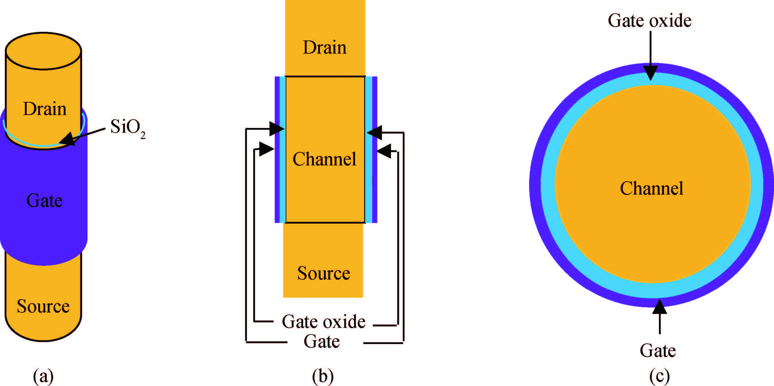
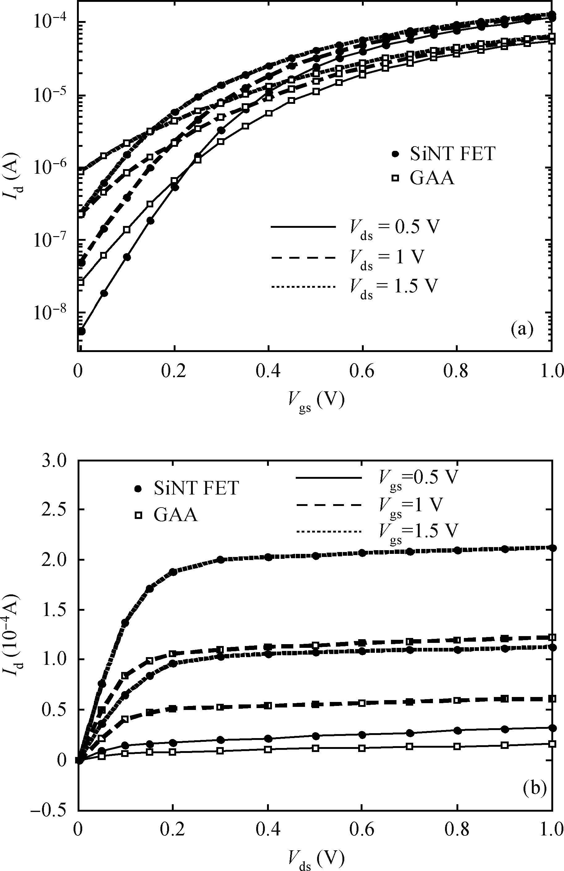
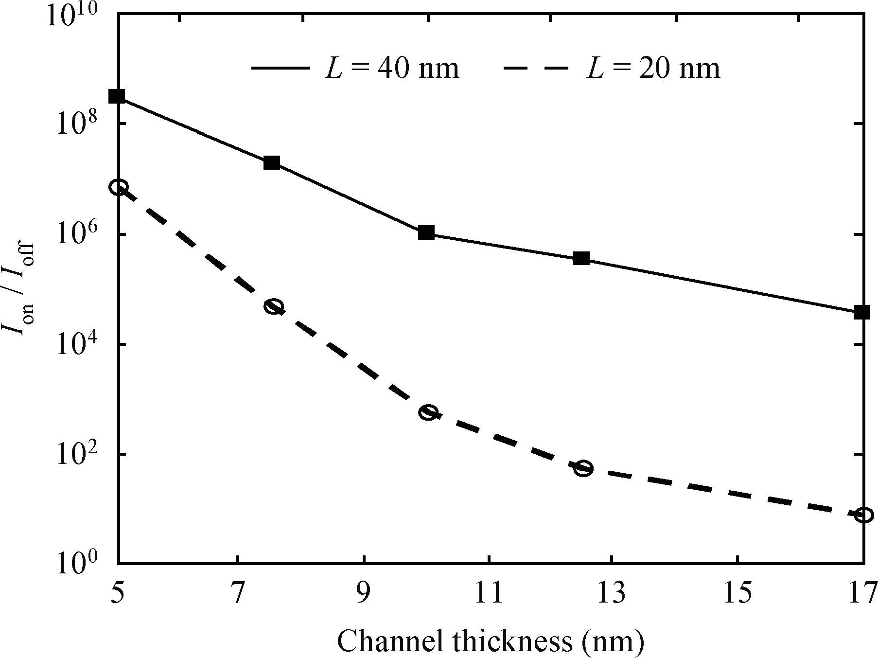
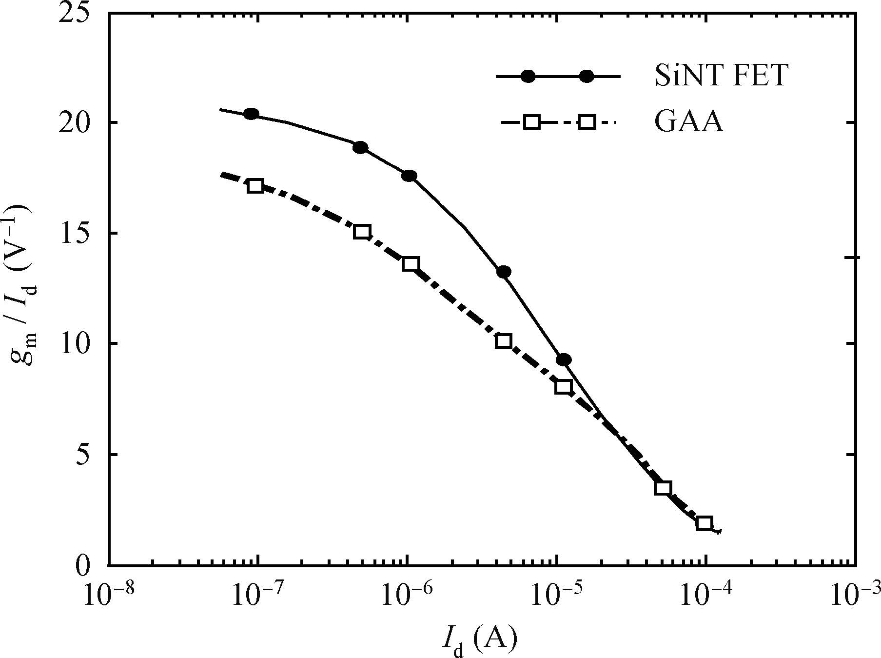
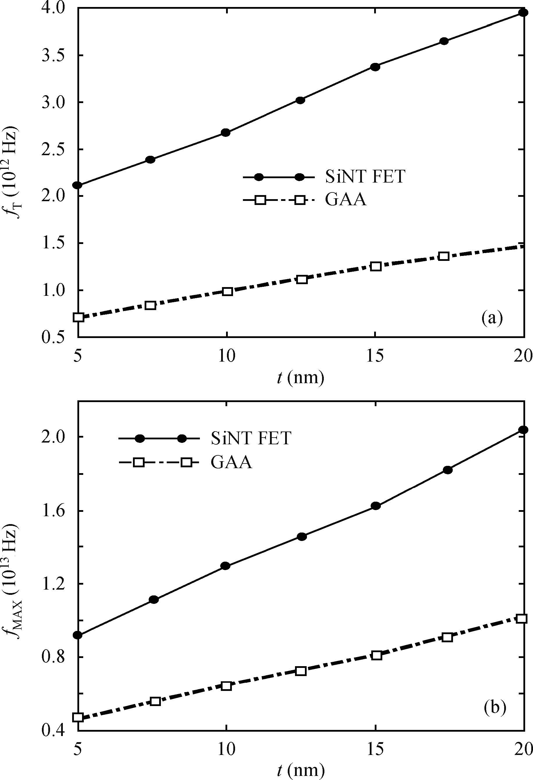
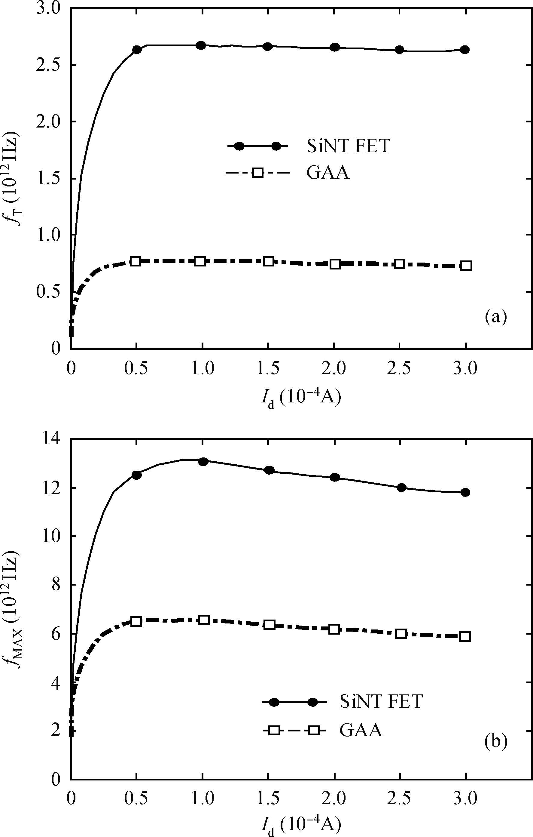
This work presents a comparative study of the influence of various parameters on the analog and RF properties of silicon-nanotube MOSFETs and nanowire-based gate-all-around (GAA) MOSFETs. The important analog and RF performance parameters of SiNT FETs and GAA MOSFETs, namely drain current (Id), transconductance to drain current ratio (gm/Id), Ion/Ioff, the cut-off frequency (fT) and the maximum frequency of oscillation (fMAX) are evaluated with the help of Y- and H-parameters which are obtained from a 3-D device simulator, ATLASTM. It is found that the silicon-nanotube MOSFETs have far more superior analog and RF characteristics (gm/Id, fT and fMAX) compared to the nanowire-based gate-all-around GAA MOSFETs. The silicon-nanotube MOSFET shows an improvement of~2.5 and 3 times in the case of fT and fMAX values respectively compared with the nanowire-based gate-all-around (GAA) MOSFET. -
References
[1] Yan H, Choe H S, Nam S, et al. Programmable nanowire circuits for nanoprocessors. Nature Lett, 2011, 470:240[2] Li M, Yeo K H, Suk S D, et al. Sub-10 nm gate-all-around CMOS nanowire transistors on bulk Si substrate. IEEE VLSI Technol Symp, 2009:94[3] Gates B D. Nanowires find their place. Nature Nano Technol, 2010, 5:484[4] Fahad H M, Hussain M M. Are nanotube architectures more advantageous than nanowire architectures for field effect transistors. Sci Report, 2012, 2:475[5] Tekleab D. Device performance of silicon nano tube field effect transistors. IEEE Electron Device Lett, 2014, 35(5):506[6] Fahad H M, Smith C E, Rojas J P, et al. Silicon nanotube field effect transistor with core-shell gate stacks for enhanced high-performance operation and area scaling benefits. Nano Lett, 2011, 11(10):4393[7] Tekleab D, Tran H H, Sleight J W, et al. Silicon nanotube MOSFET. US Patent 20120217468, 2012[8] ATLAS, A 3D device simulator from SILVACO, Singapore 2014[9] Kumar N M, Sayamal B, Sarkar C K. Influence of channel and gate engineering on the analog and RF performance of DG MOSFET. IEEE Trans Electron Device, 2010, 57(4):820 -
Proportional views