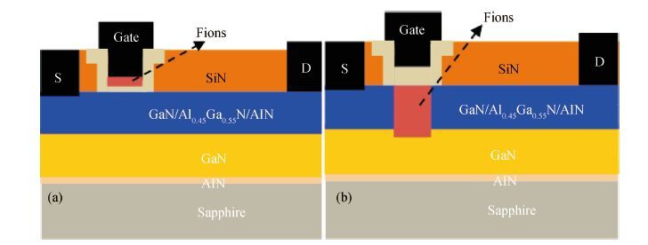
Fig. 1.
(Color online) Schematic views of (a) fluorinated-gate dielectrics MOS-HEMT and (b) conventional dielectric-last MOS-HEMT.
SEMICONDUCTOR DEVICES
Tao Gao1, 2, Ruimin Xu1, Kai Zhang2, , Yuechan Kong2, Jianjun Zhou2, Cen Kong2, Xinxin Yu2, Xun Dong2 and Tangsheng Chen2
Corresponding author: Kai Zhang, Email: haigui.34@163.com
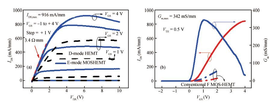
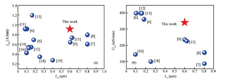
Abstract: We present high-performance enhancement-mode AlGaN/GaN metal-oxide-semiconductor high-electron mobility transistors (MOS-HEMTs) by a fluorinated gate dielectric technique. A nanolaminate of an Al2O3/LaxAl1-xO3/Al2O3 stack (x≈0.33) grown by atomic layer deposition is employed to avoid fluorine ions implantation into the scaled barrier layer. Fabricated enhancement-mode MOS-HEMTs exhibit an excellent performance as compared to those with the conventional dielectric-last technique, delivering a large maximum drain current of 916 mA/mm and simultaneously a high peak transconductance of 342 mS/mm. The balanced DC characteristics indicate that advanced gate stack dielectrics combined with buffered fluorine ions implantation have a great potential for high speed GaN E/D-mode integrated circuit applications.
Keywords: AlGaN/GaN, enhancement-mode (E-mode), stack gate dielectrics, atomic layer deposition (ALD)
| [1] |
Burnham S D, Boutros K, Hashimoto P, et al. Gate-recessed normally-off GaN-on-Si HEMT using a new O2-BCl3 digital etching technique. Phys Status Solidi C, 2010, 7(7/8):2010
|
| [2] |
Wang Y, Wang M, Xie B, et al. High-performance normally-off Al2O3/GaN MOSFET using a wet etching-based gate recess technique. IEEE Electron Devices Lett, 2013, 34(11):1370
|
| [3] |
Cai Y, Zhou Y, Chen K J, et al. High-performance enhancement-mode AlGaN/GaN HEMTs using fluorine-based plasma treatment. IEEE Electron Devices Lett, 2005, 26(7):435
|
| [4] |
Chen C, Liu X, Tian B, et al. Fabrication of enhancement-mode AlGaN/GaN MISHEMTs by using fluorinated Al2O3 as gate dielectrics. IEEE Electron Devices Lett, 2011, 32(10):1373
|
| [5] |
Zhao Y, Toyama M, Kita K, et al. Moisture-absorption-induced permittivity deterioration and surface roughness. Appl Phys Lett, 2006, 88(7):072904
|
| [6] |
Higashiwaki M, Mimura T, Matsui T. Enhancement-mode AlN/GaN HFETs using cat-CVD SiN. IEEE Trans Electron Devices, 2007, 54(6):1566
|
| [7] |
Maeda N, Hiroki M, Sasaki S, et al. High-temperature characteristics in recessed-gate AlGaN/GaN enhancement-mode heterostructure field effect transistors with enhanced-barrier structures. Jpn J Appl Phys, 2013, 52:08 JN18
|
| [8] |
Kanamura M, Ohki T, Kikkawa T, et al. Enhancement-mode GaN MIS-HEMTs with n-GaN/i-AlN/n-GaN triple cap layer and high-k gate dielectrics. IEEE Electron Devices Lett, 2010, 31(3):189
|
| [9] |
Adachi T, Deguchi T, Nakagawa A, et al. High-performance E-mode AlGaN/GaN HEMTs with LT-GaN cap layer using gate recess techniques. 66th DRC Tech Dig 2008:129
|
| [10] |
Lu B, Saadat O I, Palacios T. High-performance integrated dual gate AlGaN/GaN enhancement-mode transistor. IEEE Electron Devices Lett, 2010, 31(9):990
|
| [11] |
Corrion A L, Shinohara K, Regan D, et al. Enhancement-mode AlN/GaN/AlGaN DHFET with 700-mS/mm gm and 112-GHz fT. IEEE Electron Devices Lett, 2010, 31(10):1116
|
| [12] |
Micovic M, Tsen T, Hu M, et al. GaN enhancement/depletion-mode FET logic for mixed signal applications. Electron Lett 2005, 41(19):1081
|
| [13] |
Palacios T, Suh C S, Chakraborty A, et al. High-performance E-mode AlGaN/GaN HEMTs. IEEE Electron Devices Lett, 2006, 27(6):428
|
| [14] |
Endoh A, Yamashita Y, Ikeda K, et al. Non-recessed-gate enhancement-mode AlGaN/GaN high electron mobility transistors with high RF performance. Jpn J Appl Phys, 2004, 43(4B):2255
|
| [15] |
Singisetti U, Wong M H, Dasgupta S, et al. Enhancement-mode N-polar GaN MISFETs with self-aligned source/drain regrowth. IEEE Electron Devices Lett, 2011, 32(2):137
|
| [16] |
Lu B, Matioli E, Palacios T. Tri-gate normally-off GaN power MISFET. IEEE Electron Devices Lett, 2012, 33(3):360
|
| [17] |
Hahn H, Lükens G, Ketteniss N, et al. Recessed-gate enhancement-mode AlGaN/GaN heterostructure field-effect transistors on Si with record DC performance. Appl Phys Exp, 2011, 4:114102
|
| [18] |
Im K S, Ha J B, Kim K W, et al. Normally off GaN MOSFET based on AlGaN/GaN heterostructure with extremely high 2DEG density grown on silicon substrate. IEEE Electron Devices Lett, 2010, 31(3):192
|
| [19] |
Chu R, Chen Z, DenBaars S P, et al. V-gate GaN HEMTs with engineered buffer for normally off operation. IEEE Electron Devices Lett, 2008, 29(11):1184
|


Article views: 3896 Times PDF downloads: 49 Times Cited by: 0 Times
Received: 11 November 2015 Revised: 28 December 2015 Online: Published: 01 June 2016
| Citation: |
Tao Gao, Ruimin Xu, Kai Zhang, Yuechan Kong, Jianjun Zhou, Cen Kong, Xinxin Yu, Xun Dong, Tangsheng Chen. High-performance enhancement-mode AlGaN/GaN MOS-HEMTs with fluorinated stack gate dielectrics and thin barrier layer[J]. Journal of Semiconductors, 2016, 37(6): 064013. doi: 10.1088/1674-4926/37/6/064013
****
T Gao, R M Xu, K Zhang, Y C Kong, J J Zhou, C Kong, X X Yu, X Dong, T S Chen. High-performance enhancement-mode AlGaN/GaN MOS-HEMTs with fluorinated stack gate dielectrics and thin barrier layer[J]. J. Semicond., 2016, 37(6): 064013. doi: 10.1088/1674-4926/37/6/064013.

|
| [1] |
Burnham S D, Boutros K, Hashimoto P, et al. Gate-recessed normally-off GaN-on-Si HEMT using a new O2-BCl3 digital etching technique. Phys Status Solidi C, 2010, 7(7/8):2010
|
| [2] |
Wang Y, Wang M, Xie B, et al. High-performance normally-off Al2O3/GaN MOSFET using a wet etching-based gate recess technique. IEEE Electron Devices Lett, 2013, 34(11):1370
|
| [3] |
Cai Y, Zhou Y, Chen K J, et al. High-performance enhancement-mode AlGaN/GaN HEMTs using fluorine-based plasma treatment. IEEE Electron Devices Lett, 2005, 26(7):435
|
| [4] |
Chen C, Liu X, Tian B, et al. Fabrication of enhancement-mode AlGaN/GaN MISHEMTs by using fluorinated Al2O3 as gate dielectrics. IEEE Electron Devices Lett, 2011, 32(10):1373
|
| [5] |
Zhao Y, Toyama M, Kita K, et al. Moisture-absorption-induced permittivity deterioration and surface roughness. Appl Phys Lett, 2006, 88(7):072904
|
| [6] |
Higashiwaki M, Mimura T, Matsui T. Enhancement-mode AlN/GaN HFETs using cat-CVD SiN. IEEE Trans Electron Devices, 2007, 54(6):1566
|
| [7] |
Maeda N, Hiroki M, Sasaki S, et al. High-temperature characteristics in recessed-gate AlGaN/GaN enhancement-mode heterostructure field effect transistors with enhanced-barrier structures. Jpn J Appl Phys, 2013, 52:08 JN18
|
| [8] |
Kanamura M, Ohki T, Kikkawa T, et al. Enhancement-mode GaN MIS-HEMTs with n-GaN/i-AlN/n-GaN triple cap layer and high-k gate dielectrics. IEEE Electron Devices Lett, 2010, 31(3):189
|
| [9] |
Adachi T, Deguchi T, Nakagawa A, et al. High-performance E-mode AlGaN/GaN HEMTs with LT-GaN cap layer using gate recess techniques. 66th DRC Tech Dig 2008:129
|
| [10] |
Lu B, Saadat O I, Palacios T. High-performance integrated dual gate AlGaN/GaN enhancement-mode transistor. IEEE Electron Devices Lett, 2010, 31(9):990
|
| [11] |
Corrion A L, Shinohara K, Regan D, et al. Enhancement-mode AlN/GaN/AlGaN DHFET with 700-mS/mm gm and 112-GHz fT. IEEE Electron Devices Lett, 2010, 31(10):1116
|
| [12] |
Micovic M, Tsen T, Hu M, et al. GaN enhancement/depletion-mode FET logic for mixed signal applications. Electron Lett 2005, 41(19):1081
|
| [13] |
Palacios T, Suh C S, Chakraborty A, et al. High-performance E-mode AlGaN/GaN HEMTs. IEEE Electron Devices Lett, 2006, 27(6):428
|
| [14] |
Endoh A, Yamashita Y, Ikeda K, et al. Non-recessed-gate enhancement-mode AlGaN/GaN high electron mobility transistors with high RF performance. Jpn J Appl Phys, 2004, 43(4B):2255
|
| [15] |
Singisetti U, Wong M H, Dasgupta S, et al. Enhancement-mode N-polar GaN MISFETs with self-aligned source/drain regrowth. IEEE Electron Devices Lett, 2011, 32(2):137
|
| [16] |
Lu B, Matioli E, Palacios T. Tri-gate normally-off GaN power MISFET. IEEE Electron Devices Lett, 2012, 33(3):360
|
| [17] |
Hahn H, Lükens G, Ketteniss N, et al. Recessed-gate enhancement-mode AlGaN/GaN heterostructure field-effect transistors on Si with record DC performance. Appl Phys Exp, 2011, 4:114102
|
| [18] |
Im K S, Ha J B, Kim K W, et al. Normally off GaN MOSFET based on AlGaN/GaN heterostructure with extremely high 2DEG density grown on silicon substrate. IEEE Electron Devices Lett, 2010, 31(3):192
|
| [19] |
Chu R, Chen Z, DenBaars S P, et al. V-gate GaN HEMTs with engineered buffer for normally off operation. IEEE Electron Devices Lett, 2008, 29(11):1184
|

 WeChat ID
Journal of Semiconductors © 2017 All Rights Reserved 京ICP备05085259号-2

 DownLoad: