


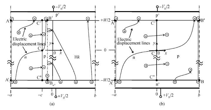
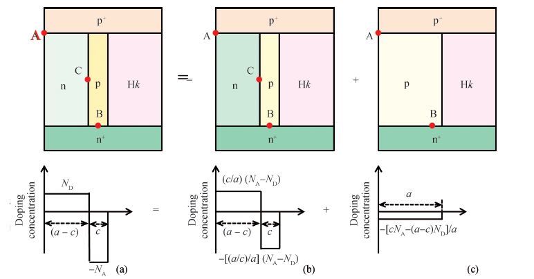
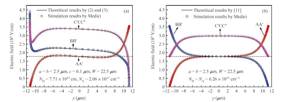
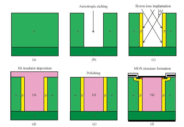
Fig. 1.
Structures of SJ voltage sustaining layers. (a) Proposed. (b) Conventional.
SEMICONDUCTOR DEVICES
Corresponding author: Mingmin Huang, mmhuang@foxmail.com
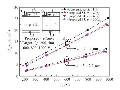
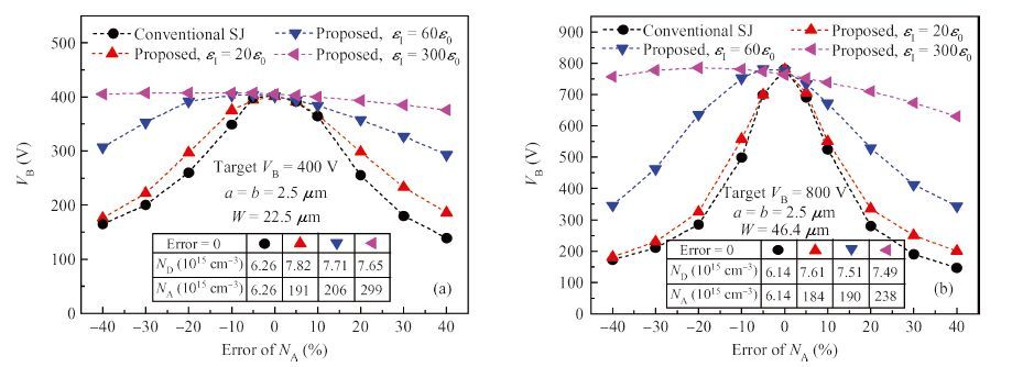
Abstract: A superjunction (SJ) structure using a high-k (Hk) insulator is studied and optimized by using an analytic model. Results by using the proposed model match well with that of numerical calculations. Numerical calculation results show that, only needing an Hk insulator with a permittivity of εI=5εS, the optimum specific on-resistance of the MOSFET applying the proposed structure is about 8%-20% lower than that of the conventional SJ-MOSFET with VB=200-1000 V. An example with VB=400 V shows that, the permissible error range of doping concentration of the p-region to maintain above 80% of VB is from -37% to +32% for the former and is only from -13% to +13% for the latter.
Keywords: high-k (Hk), superjunction MOSFET, specific on-resistance, charge imbalance
| [1] |
Coe D J. High voltage semiconductor device. US Patent, 1988:4754310
|
| [2] |
Chen X B. Semiconductor power devices with alternating conductivity type high-voltage breakdown regions. US Patent, 1993:5216275
|
| [3] |
Lorenz L, Deboy G, Knapp A, et al. COOLMOSTM-a new milestone in high voltage Power MOS. IEEE Proc ISPSD, 1999:3
|
| [4] |
Chen Y, Liang Y C, Samudra G S, et al. Progressive development of superjunction power MOSFET devices. IEEE Trans Electron Devices, 2008, 55(1):211
|
| [5] |
Napoli E, Wang H, Udrea F. The effect of charge imbalance on superjunction power devices:an exact analytical solution. IEEE Electron Devices Lett, 2008, 29(3):249
|
| [6] |
Wang H, Napoli E, Udrea F. Breakdown voltage for superjunction power devices with charge imbalance:an analytical model valid for both punch through and non punch through devices. IEEE Trans Electron Devices, 2009, 56(12):3175
|
| [7] |
Saito W. Theoretical limits of superjunction considering with charge imbalance margin. IEEE Proc ISPSD, 2015:125
|
| [8] |
Chen X B. Super-junction voltage sustaining layer with alternating semiconductor and high-k dielectric region. US patent, 2007:7230310 B2
|
| [9] |
Chen X B, Huang M M. A vertical power MOSFET with an interdigitated drift region using high-k insulator. IEEE Trans Electron Devices, 2012, 59(9):2430
|
| [10] |
Lyu X J, Chen X B. Vertical power Hk-MOSFET of hexagonal layout. IEEE Trans Electron Devices, 2013, 60(5):1709
|
| [11] |
Chen X B, Sin J K O. Optimization of the specific on-resistance of the COOLMOSTM. IEEE Trans Electron Devices, 2001, 48(2):344
|
| [12] |
Strollo A G M, Napoli E. Optimization on-resistance versus breakdown voltage tradeoff in superjunction power devices:a novel analytical model. IEEE Trans Electron Devices, 2001, 48(9):2161
|
| [13] |
Synopsys. Taurus Medici User Guide, 2010:Version D-2010.03
|
| [14] |
Modreanu M, Sancho-Parramon J, O'Connell D, et al. Solid phase crystallisation of HfO2 thin films. Mater Sci Eng B, 2005, 118(1-3):127
|
| [15] |
Ren S Q, Yang H, Tang B, et al. Characterization of positive bias temperature instability of NMOSFET with high-k/metal gate last process. Journal of Semiconductors, 2015, 36(1):014007
|
| [16] |
Shi L N, Zhuang Y Q, Li C, et al. Analytical modeling of the direct tunneling current through high-k gate stacks for long-channel cylindrical surrounding-gate MOSFETs. Journal of Semiconductors, 2014, 35(3):034009
|
| [17] |
Chandra S T, Balamurugan N B. Performance analysis of silicon nanowire transistors considering effective oxide thickness of high-k gate dielectric. Journal of Semiconductors, 2014, 35(4):044001
|
| [18] |
Bai Y R, Xu J Q, Liu L, et al. Simulation of electrical characteristics and structural optimization for small-scaled dual-gate GeOI MOSFET with high-k gate dielectric. Journal of Semiconductors, 2014, 35(9):094002
|
| [19] |
Chu F T, Chen C, Liu X Z. Breakdown voltage enhancement of AlGaN/GaN high electron mobility transistors by polyimide/chromium composite thin film passivation. Journal of Semiconductors, 2014, 35(3):034007
|
| [20] |
Pontes F M, Lee E J H, Leite E R, et al. High dielectric constant of SrTiO3 thin films prepared by chemical process. Journal of Materials Science, 2000, 35:4783
|
| [21] |
Synopsys. Taurus Tsuprem-4 User Guide, 2010:Version D-2010.03
|
| [22] |
Nitta T, Minato T, Yano M, et al. Experimental results and simulation analysis of 250 V super trench power MOSFET (STM). IEEE Proc ISPSD, 2000:77
|
| [23] |
Hattori Y, Suzuki T, Kodama M, et al. Shallow angle implantation for extended trench gate power MOSFETs with super junction structure. IEEE Proc ISPSD, 2001:427
|


Article views: 3796 Times PDF downloads: 43 Times Cited by: 0 Times
Received: 14 September 2015 Revised: 07 December 2015 Online: Published: 01 June 2016
| Citation: |
Mingmin Huang, Xingbi Chen. A superjunction structure using high-k insulator for power devices: theory and optimization[J]. Journal of Semiconductors, 2016, 37(6): 064014. doi: 10.1088/1674-4926/37/6/064014
****
M M Huang, X B Chen. A superjunction structure using high-k insulator for power devices: theory and optimization[J]. J. Semicond., 2016, 37(6): 064014. doi: 10.1088/1674-4926/37/6/064014.

|
| [1] |
Coe D J. High voltage semiconductor device. US Patent, 1988:4754310
|
| [2] |
Chen X B. Semiconductor power devices with alternating conductivity type high-voltage breakdown regions. US Patent, 1993:5216275
|
| [3] |
Lorenz L, Deboy G, Knapp A, et al. COOLMOSTM-a new milestone in high voltage Power MOS. IEEE Proc ISPSD, 1999:3
|
| [4] |
Chen Y, Liang Y C, Samudra G S, et al. Progressive development of superjunction power MOSFET devices. IEEE Trans Electron Devices, 2008, 55(1):211
|
| [5] |
Napoli E, Wang H, Udrea F. The effect of charge imbalance on superjunction power devices:an exact analytical solution. IEEE Electron Devices Lett, 2008, 29(3):249
|
| [6] |
Wang H, Napoli E, Udrea F. Breakdown voltage for superjunction power devices with charge imbalance:an analytical model valid for both punch through and non punch through devices. IEEE Trans Electron Devices, 2009, 56(12):3175
|
| [7] |
Saito W. Theoretical limits of superjunction considering with charge imbalance margin. IEEE Proc ISPSD, 2015:125
|
| [8] |
Chen X B. Super-junction voltage sustaining layer with alternating semiconductor and high-k dielectric region. US patent, 2007:7230310 B2
|
| [9] |
Chen X B, Huang M M. A vertical power MOSFET with an interdigitated drift region using high-k insulator. IEEE Trans Electron Devices, 2012, 59(9):2430
|
| [10] |
Lyu X J, Chen X B. Vertical power Hk-MOSFET of hexagonal layout. IEEE Trans Electron Devices, 2013, 60(5):1709
|
| [11] |
Chen X B, Sin J K O. Optimization of the specific on-resistance of the COOLMOSTM. IEEE Trans Electron Devices, 2001, 48(2):344
|
| [12] |
Strollo A G M, Napoli E. Optimization on-resistance versus breakdown voltage tradeoff in superjunction power devices:a novel analytical model. IEEE Trans Electron Devices, 2001, 48(9):2161
|
| [13] |
Synopsys. Taurus Medici User Guide, 2010:Version D-2010.03
|
| [14] |
Modreanu M, Sancho-Parramon J, O'Connell D, et al. Solid phase crystallisation of HfO2 thin films. Mater Sci Eng B, 2005, 118(1-3):127
|
| [15] |
Ren S Q, Yang H, Tang B, et al. Characterization of positive bias temperature instability of NMOSFET with high-k/metal gate last process. Journal of Semiconductors, 2015, 36(1):014007
|
| [16] |
Shi L N, Zhuang Y Q, Li C, et al. Analytical modeling of the direct tunneling current through high-k gate stacks for long-channel cylindrical surrounding-gate MOSFETs. Journal of Semiconductors, 2014, 35(3):034009
|
| [17] |
Chandra S T, Balamurugan N B. Performance analysis of silicon nanowire transistors considering effective oxide thickness of high-k gate dielectric. Journal of Semiconductors, 2014, 35(4):044001
|
| [18] |
Bai Y R, Xu J Q, Liu L, et al. Simulation of electrical characteristics and structural optimization for small-scaled dual-gate GeOI MOSFET with high-k gate dielectric. Journal of Semiconductors, 2014, 35(9):094002
|
| [19] |
Chu F T, Chen C, Liu X Z. Breakdown voltage enhancement of AlGaN/GaN high electron mobility transistors by polyimide/chromium composite thin film passivation. Journal of Semiconductors, 2014, 35(3):034007
|
| [20] |
Pontes F M, Lee E J H, Leite E R, et al. High dielectric constant of SrTiO3 thin films prepared by chemical process. Journal of Materials Science, 2000, 35:4783
|
| [21] |
Synopsys. Taurus Tsuprem-4 User Guide, 2010:Version D-2010.03
|
| [22] |
Nitta T, Minato T, Yano M, et al. Experimental results and simulation analysis of 250 V super trench power MOSFET (STM). IEEE Proc ISPSD, 2000:77
|
| [23] |
Hattori Y, Suzuki T, Kodama M, et al. Shallow angle implantation for extended trench gate power MOSFETs with super junction structure. IEEE Proc ISPSD, 2001:427
|

 WeChat ID
Journal of Semiconductors © 2017 All Rights Reserved 京ICP备05085259号-2

 DownLoad:

